EP0279943B1 - Gate circuit of combined field-effect and bipolar transistors - Google Patents
Gate circuit of combined field-effect and bipolar transistors Download PDFInfo
- Publication number
- EP0279943B1 EP0279943B1 EP87118836A EP87118836A EP0279943B1 EP 0279943 B1 EP0279943 B1 EP 0279943B1 EP 87118836 A EP87118836 A EP 87118836A EP 87118836 A EP87118836 A EP 87118836A EP 0279943 B1 EP0279943 B1 EP 0279943B1
- Authority
- EP
- European Patent Office
- Prior art keywords
- electrode
- conductivity type
- bipolar transistor
- base
- field
- Prior art date
- Legal status (The legal status is an assumption and is not a legal conclusion. Google has not performed a legal analysis and makes no representation as to the accuracy of the status listed.)
- Expired - Lifetime
Links
Images


Classifications
-
- H—ELECTRICITY
- H03—ELECTRONIC CIRCUITRY
- H03K—PULSE TECHNIQUE
- H03K19/00—Logic circuits, i.e. having at least two inputs acting on one output; Inverting circuits
-
- H—ELECTRICITY
- H01—ELECTRIC ELEMENTS
- H01L—SEMICONDUCTOR DEVICES NOT COVERED BY CLASS H10
- H01L27/00—Devices consisting of a plurality of semiconductor or other solid-state components formed in or on a common substrate
- H01L27/02—Devices consisting of a plurality of semiconductor or other solid-state components formed in or on a common substrate including semiconductor components specially adapted for rectifying, oscillating, amplifying or switching and having at least one potential-jump barrier or surface barrier; including integrated passive circuit elements with at least one potential-jump barrier or surface barrier
- H01L27/04—Devices consisting of a plurality of semiconductor or other solid-state components formed in or on a common substrate including semiconductor components specially adapted for rectifying, oscillating, amplifying or switching and having at least one potential-jump barrier or surface barrier; including integrated passive circuit elements with at least one potential-jump barrier or surface barrier the substrate being a semiconductor body
- H01L27/06—Devices consisting of a plurality of semiconductor or other solid-state components formed in or on a common substrate including semiconductor components specially adapted for rectifying, oscillating, amplifying or switching and having at least one potential-jump barrier or surface barrier; including integrated passive circuit elements with at least one potential-jump barrier or surface barrier the substrate being a semiconductor body including a plurality of individual components in a non-repetitive configuration
- H01L27/0611—Devices consisting of a plurality of semiconductor or other solid-state components formed in or on a common substrate including semiconductor components specially adapted for rectifying, oscillating, amplifying or switching and having at least one potential-jump barrier or surface barrier; including integrated passive circuit elements with at least one potential-jump barrier or surface barrier the substrate being a semiconductor body including a plurality of individual components in a non-repetitive configuration integrated circuits having a two-dimensional layout of components without a common active region
- H01L27/0617—Devices consisting of a plurality of semiconductor or other solid-state components formed in or on a common substrate including semiconductor components specially adapted for rectifying, oscillating, amplifying or switching and having at least one potential-jump barrier or surface barrier; including integrated passive circuit elements with at least one potential-jump barrier or surface barrier the substrate being a semiconductor body including a plurality of individual components in a non-repetitive configuration integrated circuits having a two-dimensional layout of components without a common active region comprising components of the field-effect type
- H01L27/0623—Devices consisting of a plurality of semiconductor or other solid-state components formed in or on a common substrate including semiconductor components specially adapted for rectifying, oscillating, amplifying or switching and having at least one potential-jump barrier or surface barrier; including integrated passive circuit elements with at least one potential-jump barrier or surface barrier the substrate being a semiconductor body including a plurality of individual components in a non-repetitive configuration integrated circuits having a two-dimensional layout of components without a common active region comprising components of the field-effect type in combination with bipolar transistors
-
- H—ELECTRICITY
- H03—ELECTRONIC CIRCUITRY
- H03K—PULSE TECHNIQUE
- H03K19/00—Logic circuits, i.e. having at least two inputs acting on one output; Inverting circuits
- H03K19/01—Modifications for accelerating switching
-
- H—ELECTRICITY
- H03—ELECTRONIC CIRCUITRY
- H03K—PULSE TECHNIQUE
- H03K19/00—Logic circuits, i.e. having at least two inputs acting on one output; Inverting circuits
- H03K19/01—Modifications for accelerating switching
- H03K19/017—Modifications for accelerating switching in field-effect transistor circuits
- H03K19/01707—Modifications for accelerating switching in field-effect transistor circuits in asynchronous circuits
- H03K19/01721—Modifications for accelerating switching in field-effect transistor circuits in asynchronous circuits by means of a pull-up or down element
-
- H—ELECTRICITY
- H03—ELECTRONIC CIRCUITRY
- H03K—PULSE TECHNIQUE
- H03K19/00—Logic circuits, i.e. having at least two inputs acting on one output; Inverting circuits
- H03K19/02—Logic circuits, i.e. having at least two inputs acting on one output; Inverting circuits using specified components
- H03K19/08—Logic circuits, i.e. having at least two inputs acting on one output; Inverting circuits using specified components using semiconductor devices
- H03K19/094—Logic circuits, i.e. having at least two inputs acting on one output; Inverting circuits using specified components using semiconductor devices using field-effect transistors
- H03K19/0944—Logic circuits, i.e. having at least two inputs acting on one output; Inverting circuits using specified components using semiconductor devices using field-effect transistors using MOSFET or insulated gate field-effect transistors, i.e. IGFET
- H03K19/09448—Logic circuits, i.e. having at least two inputs acting on one output; Inverting circuits using specified components using semiconductor devices using field-effect transistors using MOSFET or insulated gate field-effect transistors, i.e. IGFET in combination with bipolar transistors [BIMOS]
Definitions
- This invention relates to gate circuits formed of a combination of field-effect transistors and bipolar transistors.
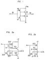
- a gate circuit formed of a combination of field-effect transistors and bipolar transistors so as to achieve high-speed operation and low-power consumption for example, an inverter circuit shown in Fig. 1 (See JP-A-54-148469).
- This inverter circuit is formed of a P-channel metal (silicon)-oxide-semiconductor field-effect-transistor (hereinafter referred to simply as PMOS) 50, an N-channel metal (silicon)-oxide-semiconductor field-effect-transistor (hereinafter referred to simply as NMOS) 51, an NPN-transistor 53, and a PNP transistor 54.
- PMOS P-channel metal (silicon)-oxide-semiconductor field-effect-transistor
- NMOS N-channel metal-oxide-semiconductor field-effect-transistor
- the bipolar transistors 53 and 54 used are complementary and difficult to be matched in their switching characteristics, the trailing edge of the output signal 56 is delayed. This is because the PNP transistor of the complementary transistors is inferior in its performances such as current amplification factor to the NPN transistor.
- This 2-input NOR circuit is a combination of a C-MOS transistor NOR gate circuit having PMOSs 200 and 201 and NMOSs 202 and 203 as shown in Fig. 2b, and NPN transistors 301 and 302.
- the time required for the switching from the ON-state to the OFF-state is long because here are no means for forcibly extracting or drawing out minority charges accumulated on the bases of the NPN transistors 301 and 302.
- the first and second NPN transistors 301 and 302 remain long in the ON-state, so that the switching time as well as the power consumption increase.
- US-A-4 225 877 discloses an integrated circuit with C-MOS logic and a bipolar driver with polysilicon resistors.
- the structure of the semiconductor devices such as feed-transistors FET-transistors and bipolar transistors disclosed in this document is not sufficient to enable low power and high frequency switching properties of the circuit. This results from the fact that the bipolar transistors are not isolated from other semiconductor devices, thus increasing power consumption.
- the structure is related to another circuit as compared to that of the present invention.
- the French document FR-A-2 449 334 discloses a method for monolithic integration of circuits. It discloses general considerations of how a monolithic integrated circuit has to be fabricated. As examples a driving circuit for a plasma display and a programmable current source are given.
- the gate circuit according to the invention is integrated in a semiconductor substrate having a first and a second main surface. All electrodes of gates, drains, sources, collectors, emitters, bases and of the discharge means are formed on the first main surface.
- the inverter circuit shown in Fig. 3 comprises a first bipolar NPN transistor 14 having its collector electrode C connected to a power supply terminal 1 at which a first fixed potential V DD is maintained, and its emitter electrode E connected to an output terminal 17.
- the collector electrode C of a second bipolar NPN transistor 15 is connected to the output terminal 17 and its emitter electrode E connected to ground potential GND as a second fixed potential.
- the gate electrode G of a P-channel metal (silicon)-oxide-semiconductor field-effect-transistor (hereinafter, referred to simply as PMOS) 10 is connected to an input terminal 16, its source electrode S and its drain electrode D being respectively connected to the collector electrode C and the base electrode B of the first NPN transistor 14.
- PMOS P-channel metal (silicon)-oxide-semiconductor field-effect-transistor
- the circuit comprises an N-channel metal (silicon)-oxide-semiconductor field-effect transistor (hereinafter, referred to simply as NMOS) 11 having its gate electrode G connected to the input terminal 16, and its drain electrode D and source electrode S respectively connected to the collector electrode C and the base electrode B of the second NPN transistor 15.
- NMOS N-channel metal (silicon)-oxide-semiconductor field-effect transistor
- a resistor 12 connects the drain electrode D of the PMOS 10 with the drain electrode D of the NMOS 11, and the resistor 13 connects the base electrode B with the emitter electrode E of the second NPN transistor 15.
- Fig. 4 schematically shows the cross-section of the implementation of the inverter circuit illustrated in Fig. 3 in a semiconductor integrated circuit structure according to the invention.
- the PMOS 10, the first NPN transistor 14, resistors 12 and 13 and the NMOS 11 are formed in an island 212 of a semiconductor substrate 210, and the second NPN transistor 15 in an island 213 thereof.
- a buried layer 227 is provided below these transistor structures.
- a P+-region 219 and a gate electrode G constitute the PMOS 10
- an N+-region 223 and a gate electrode G within a P well 214 constitute the NMOS 11.
- the first NPN transistor 14 comprises a P-region 217 as its base, and N+-region 218 within the P-region 217 as its emitter and an N+-region 215 as its collector.
- the second NPN transistor 15 comprises a P-region 225 within the island 213 as its base, an N+-region 226 within the P-region 225 as its emitter, and an N+-region 224 as its collector.
- the corresponding electrodes of the NPN transistors 14 and 15 are designated with B, E and C, respectively.
- the PMOS 10 When the input terminal 16 is at "0" level, the PMOS 10 is turned on but the NMOS 11 off. Thus, the base potential of the first NPN transistor 14 increases to turn on the NPN transistor 14. At this time, since the NMOS 11 is turned off, the current to the second NPN transistor 15 is stopped, and the charges accumulated in the base B of the second NPN transistor 15 are drawn out through the resistor 13 to the ground, so that the second NPN transistor 15 is rapidly turned off.
- the emitter current of the first NPN transistor 14 charges the load (not shown), and the output terminal 17 rapidly becomes "1" level.
- the PMOS 10 When the input terminal 16 is at "1" level, the PMOS 10 is made off but the NMOS 11 on. At this time, since the PMOS 10 is off, the current to the NPN transistor 14 stops, and the charges stored on the base of the first NPN transistor 14 and in the drain of the PMOS 10 are drawn out through the resistors 12 and 13 to the ground, so that the first NPN transistor 14 is rapidly turned off.
- the NMOS 11 since the NMOS 11 is on to form a short-circuit between its drain electrode D and its source electrode S, the second NPN transistor 15 is supplied at its base electrode B with the current from the output terminal 17 and with the charges stored in the base of the first NPN transistor 14 and in the drain of the PMOS 10 as mentioned above, and thereby the NPN transistor 15 is rapidly turned on. Consequently, the output terminal 17 rapidly reaches "0" level.
- the resistor 12 extracts the charges accumulated in the drain of the PMOS 10 and in the base of the first NPN transistor 14 to rapidly turn off the first NPN transistor 14, and supplies the extracted charges via the NMOS 11 in the ON-state to the base electrode B of the second NPN transistor 15 to rapidly turn on the second NPN transistor 15.
- the resistor 12 is provided between the drain of the PMOS 10 and the drain of the NMOS 11, a conductive path for causing short-circuiting is not formed between the power supply terminal 1 and GND, and thus low-power consumption in the C-MOS circuit can be achieved.
- the resistor 12 were connected between the drain of the PMOS 10 and GND, a conductive path would be formed between the power supply terminal 1 and GND when the input terminal 16 is at "0" level, and thus current would always flow therethrough to increase power consumption.
- the resistor 12 is also connected to the output terminal 17, the potential at the output terminal 17, when the input terminal 16 is at "0" level, can be raised to the potential at the power supply terminal 1 through the PMOS 10 and the resistor 12, thus assuring enough noise immunity.
- the resistor 13 when the NMOS 11 and the second NPN transistor 15 are switched from the ON-state to the OFF-state, discharges the charges accumulated in the base of the second NPN transistor 15 so as to rapidly turn off the second NPN transistor 15. Also, in this embodiment, when the input terminal 16 is at "1" level, the output terminal 17 can be brought to "0" level through the resistor 13 and the NMOS 11, thus assuring enough noise immunity.
- the bipolar transistors used are of the same NPN-type, which is advantageous for obtaining uniform switching characteristics.
- the output signal shows no trailing effect, and thus high-speed operation is ensured.
- Fig. 5 shows a 2-input NAND circuit according to the parent patent to which this invention can be applied.
- This circuit comprises a first NPN transistor 26 having its collector electrode C connected to the power supply terminal 1, and its emitter electrode E connected to an output terminal 29, a second NPN transistor 27 having its collector electrode C connected to an output terminal 29 and its emitter electrode E connected to ground potential GND, and two input terminals 28.
- the gate electrodes G of PMOSs 20 and 21 are respectively connected to one and the other of the input terminals 28, their source - drain paths being connected in parallel between the collector electrode C and the base electrode B of the first NPN transistor 26; the gate electrodes G of NMOSs 22 and 23 are respectively connected to one and the other of the input terminals 28, and their drain - source paths are connected in series between the collector electrode C and the base electrode B of the second NPN transistor 27.
- a resistor 24 is connected between the common drain of the PMOSs 20 and 21 and the drain of the NMOS 22, and a resistor 25 is connected between the base and the emitter of the second NPN transistor 27.
- Table 2 shows the logic operation of this embodiment.
- the emitter current of the first NPN transistor 26 charges the load to rapidly raise the potential of the output terminal 29 to "1" level.
- both of the input terminals 28 are at "0" level, both the PMOSs 20 and 21 are turned on, and both the NMOSs 22 and 23 are turned off. Thus, the operation is the same as above, the output terminal 29 reaching "1" level.
- both the input terminals 28 are at "1" level
- both of the PMOSs 20 and 21 are turned off, and both NMOSs 22 and 23 are turned on.
- the current to the first NPN 26 stops flowing, and the charges accumulated in the base of the first NPN transistor 26 are extracted, so that it is rapidly turned off.
- the NMOSs 22 and 23 are turned on to form short-circuit-between the drains and sources the second NPN transistor 27 is supplied at its base electrode B with the current from the output terminal 29 and with discharge current from the base electrode B of the first NPN transistor 26 as described previously so as to rapidly turn it on.
- the output terminal 29 rapidly reaches "0" level.
- Fig. 6 shows a 2-input NOR circuit according to the parent patent to which this invention can be applied.
- This circuit comprises a first NPN transistor 36 having its collector electrode C connected to the power supply terminal 1 and its emitter electrode E connected to the output terminal 39, and a second NPN transistor 37 having its collector electrode C connected to the output terminal 39 and its emitter electrode E connected to ground potential GND.
- the gate electrodes G of two PMOSs 30 and 31 are connected to one and the other of the input terminals 38 and their source - drain paths connected in series between the collector electrode C and the base electrode B of the first NPN transistor 36.
- NMOSs 32 and 33 have their gate electrodes G connected to one and the other of the input terminals 38 and the drain - source paths connected in parallel between the collector electrode C and the base electrode B of the second NPN transistor 37.
- a resistor 34 connects the drain electrode D of the PMOS 31 with the drain electrodes D of the NMOSs 32 and 33, and a resistor 35 connects the base electrode B to the emitter electrode E of the second NPN transistor 37.
- Table 3 shows the logic operation of this circuit.
- both of the input terminals 38 are at "0" level, both the PMOSs 30 and 31 are turned on, and both the NMOSs 32 and 33 are turned off.
- the base potential of the first NPN transistor 36 increases, and as a result the NPN transistor 36 is turned on.
- both the NMOSs 32 and 33 are turned off, the current to the second NPN transistor 37 stops flowing, and the charges accumulated in the base of the second NPN transistor 37 are extracted, so that it is rapidly turned off.
- the emitter current of the first NPN transistor 36 charges the load to rapidly raise the output terminal 39 to "1" level.
- either of the input terminals 38 is at "1" level
- either of the PMOSs 30 and 31 is turned off, and either of the NMOSs 32 and 33 is turned on.
- the current to the first NPN transistor 36 stops flowing, and the charges accumulated in the base of the first NPN transistor 36 are extracted, so that this transistor is rapidly turned off.
- the second NPN transistor 37 is supplied at its base electrode B with the current from the output terminal 39 and with the current of the charges accumulated in the base of the first NPN transistor 36 and in either of the PMOSs 30 and 31, thus rapidly turning it on. Therefore, the output terminal 39 rapidly raises to "0" level.
- both input terminals 38 are at "1" level, both the PMOSs 30 and 31 are turned off, and both the NMOSs 32 and 33 are turned on. Consequently, the operation is the same as above, the output terminal 39 being at "0" level.
- Fig. 7 shows a latch circuit using at its output the inverter circuit shown in Fig. 3.
- the circuit of Fig. 7 comprises a CMOS inverter 42 for reversing a latch pulse provided at terminal 401, a transfer gate 40 for transmitting data from the data input 400, a CMOS inverter 43 constituting a memory portion, and a transfer gate 41.
- CMOS inverter 42 for reversing a latch pulse provided at terminal 401
- transfer gate 40 for transmitting data from the data input 400
- CMOS inverter 43 constituting a memory portion
- a transfer gate 41 a transfer gate 41.
- the latch pulse at terminal 401 is made "1". Then, the transfer gate 40 is turned on, and the transfer gate 41 is turned off, so that the data are written. Thereafter, when the latch pulse is made "0", the transfer gate 40 is turned off, and the transfer gate 41 is turned on. Consequently, the data are held by the inverter 43, the totem pole output type inverter and the transfer gate 41.
- the latch circuit can be formed by the smallest configuration of a CMOS drive stage and two bipolar output stages as a high-speed, low-power consumption and high-density LSI.
- Fig. 8 shows an inverter circuit according to the parent patent to which this invention can be applied.
- the resistor 12 shown in the embodiment of Fig. 3 is replaced by a second N-channel metal (silicon)-oxide-semiconductor field-effect transistor 90 (hereinafter, simply referred to as second NMOS 90), the NMOS 11 being the first NMOS.
- the second NMOS 90 has its gate electrode G connected to the input terminal 16, and its drain electrode D and its source electrode S connected to the drain electrode D of the PMOS 10 and the base electrode B of the second NPN transistor 15, respectively.
- Like elements corresponding to those of Fig. 3 are identified by the same reference numerals.
- the operation of the inverter of Fig. 8 is substantially the same as in the case of Fig. 3.
- the circuit of Fig. 8 is different from that of Fig. 3 in that when the first NPN transistor 14 is turned off, or when the input terminal 16 is at "1" level, the second NMOS 90 is turned on, to discharge the charges accumulated in the first NPN transistor 14.
- the source electrode S of the second NMOS 90 is connected to the base electrode B of the second NPN transistor 15 so that the base current is increased to accelerate the switsching of the second NPN transistor 15 from the OFF-state to the ON-state.
- the source electrode S of the second NMOS 90 may be connected to the drain electrode D of the first NMOS 11.
- the current flows through the resistor 12 when the PMOS 10 is switched from the OFF-state to the ON-state, to delay the rise of the base potential of the first NPN transistor 14, and thus to somewhat delay the switching of the first NPN transistor 14 from the OFF-state to the ON-state, but in this embodiment when the PMOS 10 is turned on from the OFF-state the second NMOS 90 is turned off from the ON-state so that no current flows between drain and source of the NMOS 90.
- the base potential of the first NPN transistor 14 rises faster than in the first embodiment, to accelerate the switching of the NPN transistor 14 from the OFF- to the ON-state.
- the second NMOS 90 is used in place of the resistor 12, so as to improve the integration density and the operation speed. Since the source S of the second NMOS 90 is connected to the base of the second NPN transistor 15, the operation speed is further improved.
- Fig. 9 shows an inverter circuit according to the parent patent to which this invention can be applied.
- the resistor 13 of the circuit of Fig. 8 is replaced by a P-channel junction field-effect transistor (hereinafter, referred to as PJFET) 100 as a second P-channel field-effect transistor.
- PJFET P-channel junction field-effect transistor
- the gate of the PJFET 100 is connected to the input terminal 16, and the source and the drain thereof are connected to the base and to the emitter of the second NPN transistor 15, respectively.
- Fig. 9 is different from the circuit of Fig. 8 in that when the second NPN transistor 15 is turned off from the ON-state, or when the input terminal 16 is changed from level "1" to "0" level, the charges accumulated in the second NPN transistor 15 are extracted through the PJFET 100. When the charges are discharged, the ON-resistance of the PJFET 100 is decreased to accelerate the switching of the second NPN transistor 15 from the ON-state to the OFF-state.
- the PJFET 100 When the input terminal 16 changes from “0" to "1" level, the PJFET 100 is changed rom the ON-state to the OFF-state, and thus the base current to the second NPN transistor 15 is not shunted so that the second NPN transistor 15 is rapidly turned on from the OFF-state.
- This embodiment provides a much higher speed as compared with the previously described embodiments.
- Fig. 10 shows an inverter circuit according to the parent application to which this invention can be applied.
- third NMOS 110 N-channel metal oxide-semiconductor field-effect-transistor
- the third NMOS 110 has its gate electrode G connected to the base electrode B of the first NPN transistor 14, and its drain electrode D and its source electrode S connected to the base electrode B and the emitter electrode E of the second NPN transistor 15, respectively.
- This embodiment is different from the circuit of Fig. 8 in that when the second NPN transistor 15 is turned off from the ON-state, or when the input terminal 16 is changed from "1" to "0" level, the charges accumulated in the second NPN transistor 15 are extracted through the third NMOS 110.
- the high base potential of the first NPN transistor 14 is applied to the gate of the third NMOS 110, which then turns on to form short circuit between the base and emitter of the second NPN transistor 15, thus extracting the accumulated charges more rapidly.
- the above described logic circuits can be used for implementation in LSIs according to this invention, which in turn can be applied to output buffer circuits for driving an external circuit. Examples of such applications are shown in Figs. 11, 12 and 13. Although these three examples are inverter circuits, the buffer circuit may also be a multi-input NAND or a multi-input NOR circuit.
- Fig. 11 shows an inverter circuit according to a first embodiment of this invention. This circuit has substantially the same construction and operates in a similar manner as the circuit of Fig. 8.
- the circuit comprises a first NPN transistor 125 with a Schottky barrier diode provided between the base and collector as compared with the first NPN transistor 14 in Fig. 8, a second NPN transistor 126 with a Schottky barrier diode provided between the base and collector as compared with the second NPN transistor 15 of Fig.
- fourth NMOS N-channel metal (silicon)-oxide-semiconductor field-effect-transistor
- This embodiment is different from the circuit of Fig. 8 in that the first and second NPNs 125 and 126, respectively, have a Schottky barrier diode added for the purpose of accelerating the time of extraction of accumulated charges, due to the saturation of the NPN transistors.
- this embodiment is different from the circuit of Fig. 8 in that according to the invention the fourth NMOS 123 is provided between the power supply terminal 1 and the base electrode B of the second NPN transistor 126, with its gate electrode G being connected to the input terminal 16.
- the fourth NMOS 123 is provided between the power supply terminal 1 and the base electrode B of the second NPN transistor 126, with its gate electrode G being connected to the input terminal 16.
- a high-speed, low-power consumption inverting output circuit can be realized.
- Fig. 12 shows an inverter circuit according to a second embodiment of this invention. This circuit has substantially the same construction and operates in a similar manner as the circuit of Fig. 9.
- Fig. 12 like elements corresponding to those of Figs. 9 and 11 are identified by the same reference numerals.
- the resistor 13 in Fig. 11 is replaced by a PJFET 100 as in Fig. 9.
- This circuit is different from the circuit of Fig. 9 in that, as in the embodiment of Fig. 11, the first and second NPN transistors 125 and 126 have a Schottky barrier diode added, and in that the fourth NMOS 123 is provided for supplying current to the base of the second NPN transistor 126.
- an inverting output circuit operating at a much higher-speed can be realized.
- Fig. 13 shows an inverter circuit of a third embodiment of this invention.
- This circuit has substantially the same construction and operates in a similar manner as the circuit of Fig. 10.
- like elements corresponding to those of Figs. 10 and 11 are identified by the same reference numerals.
- the resistor 13 in the circuit of Fig. 11 is replaced by the third NMOS 110.
- This embodiment is different from the circuit of Fig. 10 in that as in the first embodiment of Fig. 11, the first and second NPN transistors 125 and 126 have a Schottky barrier diode added, and in that the fourth NMOS 123 is provided for supplying current to the base of the second NPN transistor 126. According to this embodiment, inverting output circuits having a much higher integration density can be realized.
- Fig. 14 shows an inverter circuit according to the parent patent to which this invention can be applied.
- This circuit comprises a bipolar PNP transistor (hereinafter, simply referred to as second PNP) 114 having its emitter electrode E connected to the power supply terminal 1 at which the fixed potential is kept, and its collector electrode C connected to the output terminal 17, and bipolar PNP transistor (hereinafter, simply referred to as first PNP) 115 having its emitter electrode E connected to the output terminal 17 and its collector electrode C connected to a fixed ground potential GND.
- the PMOS 11 has its gate electrode G connected to the input terminal 16, and its source electrode S and its drain electrode D respectively connected to the base electrode B and the collector electrode C of the second PNP transistor 114.
- the NMOS 10 has its gate electrode G connected to the input terminal 16 and its drain electrode D and its source electrode S respectively connected to the base electrode B and the collector electrode C of the first PNP transistor 115.
- the resistor 12 connects the drain electrode D of the PMOS 11 to that of the NMOS 10.
- the resistor 13 connects the base electrode B to the emitter electrode E of the second PNP transistor 114.
- bipolar NPN transistors 14 and 15 of the circuit of Fig. 3 are replaced by the bipolar PNP transistors 115 and 114, respectively, whereby the same operation is performed.
- Fig. 15 shows a 2-input NAND circuit according to the parent patent to which this invention can be applied.
- This circuit comprises a second PNP transistor 326 having its emitter electrode E connected to the power supply terminal 1 and its collector electrode C connected to the output terminal 29, a first PNP transistor 327 having its emitter electrode E connected to the output terminal 29 and its collector electrode C connected to the ground potential GND, two input terminals 28, and PMOSs 22 and 23 having their gate electrodes G connected to one and the other of the input terminals 28, respectively, and their source-drain paths connected in parallel between the base electrode B and the collector electrode C of the second PNP transistor 326.
- NMOSs 20 and 21 having their gate electrodes G respectively connected to one and the other of the input terminals 28 and their drain-source paths connected in series between the base electrode B and the collector electrode C of the first PNP transistor 327, a resistor 24 connecting the drain electrode D of the PMOSs 22 and 23 with the drain electrode D of the NMOS 20, and a resistor 25 connecting the base electrode B and the emitter electrode E of the second PNP transistor 326.
- bipolar NPN transistors 26 and 27 in the circuit of Fig. 5 are replaced by the bipolar PNP transistors 327 and 326, respectively, whereby the same operation as in this embodiment is performed.
- Fig. 16 shows a 2-input NOR circuit according to the parent patent to which this invention can be applied.
- the circuit comprises a second PNP transistor 436 having its emitter electrode E connected to the power supply terminal 1 and its collector electrode C connected to the output terminal 39, a first PNP transistor 437 having its emitter electrode E connected to the output terminal 39 and its collector electrode C connected to the ground potential GND, two input terminals 38, PMOSs 32 and 33 having their gate electrodes G connected to one and the other of the input terminals 38, respectively, and their source-drain paths connected in series between the base electrode B and the collector electrode C of the second PNP transistor 436, and NMOSs 30 and 31 having their gate electrodes G connected to one and the other of the input terminals 38, respectively, and their drain-source paths connected in parallel between the base electrode B and the collector electrode C of the first PNP transistor 437.
- it comprises a resistor 34 connecting the drain electrode D of the PMOS 33 to the drain electrodes D of the NMOSs 30 and 31, and a resistor 35 connecting the base electrode B to the emitter electrode E of the second PNP transistor 436.
- the bipolar NPN transistors 36 and 37 in the circuit of Fig. 6 are replaced by the bipolar PNP transistors 437 and 436, respectively, whereby the same operation as in the third embodiment is performed.
- logic gates are only NAND and NOR circuits, it will easily be understood that other logic gate circuits such as AND and OR circuits, logic circuit combinations, flip-flops or shift registers can be formed by connecting a logic gate circuit of, for example, CMOS transistors to the input side of the NAND and NOR circuits.
Description
- This invention relates to gate circuits formed of a combination of field-effect transistors and bipolar transistors.
- There is known a gate circuit formed of a combination of field-effect transistors and bipolar transistors so as to achieve high-speed operation and low-power consumption, for example, an inverter circuit shown in Fig. 1 (See JP-A-54-148469).
- This inverter circuit is formed of a P-channel metal (silicon)-oxide-semiconductor field-effect-transistor (hereinafter referred to simply as PMOS) 50, an N-channel metal (silicon)-oxide-semiconductor field-effect-transistor (hereinafter referred to simply as NMOS) 51, an NPN-
transistor 53, and aPNP transistor 54. - In this inverter circuit, when the
input 55 is at "0" level, the PMOS 50 is turned on but theNMOS 51 off. Consequently, the base potential of theNPN transistor 53 and thePNP transistor 54 is increased to turn on theNPN transistor 53 but turn off thePNP transistor 54, and thus theoutput 56 becomes "1" level. When theinput 55 is at "1" level, the PMOS 50 is turned off but theNMOS 51 on. Consequently, the base potential of theNPN transistor 53 and thePNP transistor 54 is reduced to turn off theNPN transistor 53 but turn on thePNP transistor 54, and thus theoutput 56 becomes "0" level. - However, since the
bipolar transistors output signal 56 is delayed. This is because the PNP transistor of the complementary transistors is inferior in its performances such as current amplification factor to the NPN transistor. - There is also known a 2-input NOR gate circuit shown in Fig. 2a (IEEE. Trans. Electron Devices, vol. ED-16, No. 11, pp. 945-951, Nov. 1969). This 2-input NOR circuit is a combination of a C-MOS transistor NOR gate
circuit having PMOSs NMOSs NPN transistors NPN transistors NPN transistors second NPN transistors - US-A-4 225 877 discloses an integrated circuit with C-MOS logic and a bipolar driver with polysilicon resistors. However, the structure of the semiconductor devices such as feed-transistors FET-transistors and bipolar transistors disclosed in this document is not sufficient to enable low power and high frequency switching properties of the circuit. This results from the fact that the bipolar transistors are not isolated from other semiconductor devices, thus increasing power consumption. Moreover, the structure is related to another circuit as compared to that of the present invention.
- The French document FR-A-2 449 334 discloses a method for monolithic integration of circuits. It discloses general considerations of how a monolithic integrated circuit has to be fabricated. As examples a driving circuit for a plasma display and a programmable current source are given.
- It is the object of the present invention to provide a BiCMOS integrated circuit device which provides high-speed operation and high packing density and which has a low power consumption.
- This object is solved in accordance with the features of
Claim 1. The dependent claims relate to preferred embodiments of the present invention. - According to one embodiment, the gate circuit according to the invention is integrated in a semiconductor substrate having a first and a second main surface. All electrodes of gates, drains, sources, collectors, emitters, bases and of the discharge means are formed on the first main surface.
- The invention will be explained with reference to preferred embodiments and the accompanying drawings, wherein for a better understanding and because of the relation between the parent patent and the present subject-matter concerning the claim features A) to H) reference is also made to the subject-matter of the parent patent, because the concept of this invention can be applied to the circuit principle according to the parent patent.
- Fig. 3 is a circuit diagram showing a logic gate circuit in the form of an inverter according to the parent patent;
- Fig. 4 is a schematic diagram showing a cross-section of the logic gate circuit of Fig. 3, implemented in an integrated circuit structure according to this invention;
- Figs. 5 - 7 are circuit diagrams showing NAND, NOR and latch circuits, respectively, according to the parent patent;
- Figs. 8 - 10 are circuit diagrams showing inverter circuits according to the parent patent;
- Figs. 11 - 13 are circuit diagrams of inverter circuits according to different embodiments of this invention; and
- Figs. 14 - 16 are circuit diagrams of inverter NAND and NOR circuits, respectively, according to the parent patent.
- The inverter circuit shown in Fig. 3 comprises a first
bipolar NPN transistor 14 having its collector electrode C connected to apower supply terminal 1 at which a first fixed potential VDD is maintained, and its emitter electrode E connected to anoutput terminal 17. The collector electrode C of a secondbipolar NPN transistor 15 is connected to theoutput terminal 17 and its emitter electrode E connected to ground potential GND as a second fixed potential. The gate electrode G of a P-channel metal (silicon)-oxide-semiconductor field-effect-transistor (hereinafter, referred to simply as PMOS) 10 is connected to aninput terminal 16, its source electrode S and its drain electrode D being respectively connected to the collector electrode C and the base electrode B of thefirst NPN transistor 14. Furthermore, the circuit comprises an N-channel metal (silicon)-oxide-semiconductor field-effect transistor (hereinafter, referred to simply as NMOS) 11 having its gate electrode G connected to theinput terminal 16, and its drain electrode D and source electrode S respectively connected to the collector electrode C and the base electrode B of thesecond NPN transistor 15. Aresistor 12 connects the drain electrode D of thePMOS 10 with the drain electrode D of theNMOS 11, and theresistor 13 connects the base electrode B with the emitter electrode E of thesecond NPN transistor 15. - Fig. 4 schematically shows the cross-section of the implementation of the inverter circuit illustrated in Fig. 3 in a semiconductor integrated circuit structure according to the invention. The
PMOS 10, thefirst NPN transistor 14,resistors NMOS 11 are formed in anisland 212 of asemiconductor substrate 210, and thesecond NPN transistor 15 in anisland 213 thereof. - Below these transistor structures a buried
layer 227 is provided. A P⁺-region 219 and a gate electrode G constitute thePMOS 10, and an N⁺-region 223 and a gate electrode G within aP well 214 constitute theNMOS 11. Thefirst NPN transistor 14 comprises a P-region 217 as its base, and N⁺-region 218 within the P-region 217 as its emitter and an N⁺-region 215 as its collector. Thesecond NPN transistor 15 comprises a P-region 225 within theisland 213 as its base, an N⁺-region 226 within the P-region 225 as its emitter, and an N⁺-region 224 as its collector. The corresponding electrodes of theNPN transistors - In table 1 the logic operation of the inverter circuit of this embodiment are indicated.

- When the
input terminal 16 is at "0" level, thePMOS 10 is turned on but theNMOS 11 off. Thus, the base potential of thefirst NPN transistor 14 increases to turn on theNPN transistor 14. At this time, since theNMOS 11 is turned off, the current to thesecond NPN transistor 15 is stopped, and the charges accumulated in the base B of thesecond NPN transistor 15 are drawn out through theresistor 13 to the ground, so that thesecond NPN transistor 15 is rapidly turned off. - Therefore, the emitter current of the
first NPN transistor 14 charges the load (not shown), and theoutput terminal 17 rapidly becomes "1" level. - When the
input terminal 16 is at "1" level, thePMOS 10 is made off but theNMOS 11 on. At this time, since thePMOS 10 is off, the current to theNPN transistor 14 stops, and the charges stored on the base of thefirst NPN transistor 14 and in the drain of thePMOS 10 are drawn out through theresistors first NPN transistor 14 is rapidly turned off. In addition, since theNMOS 11 is on to form a short-circuit between its drain electrode D and its source electrode S, thesecond NPN transistor 15 is supplied at its base electrode B with the current from theoutput terminal 17 and with the charges stored in the base of thefirst NPN transistor 14 and in the drain of thePMOS 10 as mentioned above, and thereby theNPN transistor 15 is rapidly turned on. Consequently, theoutput terminal 17 rapidly reaches "0" level. - The function of the
resistor 12 will further be described. When thePMOS 10 and thefirst NPN transistor 14 are switched from the ON-state to the OFF-state, theresistor 12 extracts the charges accumulated in the drain of thePMOS 10 and in the base of thefirst NPN transistor 14 to rapidly turn off thefirst NPN transistor 14, and supplies the extracted charges via theNMOS 11 in the ON-state to the base electrode B of thesecond NPN transistor 15 to rapidly turn on thesecond NPN transistor 15. - In addition, since the
resistor 12 is provided between the drain of thePMOS 10 and the drain of theNMOS 11, a conductive path for causing short-circuiting is not formed between thepower supply terminal 1 and GND, and thus low-power consumption in the C-MOS circuit can be achieved. In other words, if theresistor 12 were connected between the drain of thePMOS 10 and GND, a conductive path would be formed between thepower supply terminal 1 and GND when theinput terminal 16 is at "0" level, and thus current would always flow therethrough to increase power consumption. - Moreover, in this embodiment, since the
resistor 12 is also connected to theoutput terminal 17, the potential at theoutput terminal 17, when theinput terminal 16 is at "0" level, can be raised to the potential at thepower supply terminal 1 through thePMOS 10 and theresistor 12, thus assuring enough noise immunity. - The function of the
resistor 13 will hereinafter be described. As mentioned before, theresistor 13, when theNMOS 11 and thesecond NPN transistor 15 are switched from the ON-state to the OFF-state, discharges the charges accumulated in the base of thesecond NPN transistor 15 so as to rapidly turn off thesecond NPN transistor 15. Also, in this embodiment, when theinput terminal 16 is at "1" level, theoutput terminal 17 can be brought to "0" level through theresistor 13 and theNMOS 11, thus assuring enough noise immunity. - Moreover, in this embodiment, the bipolar transistors used are of the same NPN-type, which is advantageous for obtaining uniform switching characteristics.
- Furthermore, in this embodiment, since no PNP transistor with low current amplification is used, the output signal shows no trailing effect, and thus high-speed operation is ensured.
- Fig. 5 shows a 2-input NAND circuit according to the parent patent to which this invention can be applied. This circuit comprises a
first NPN transistor 26 having its collector electrode C connected to thepower supply terminal 1, and its emitter electrode E connected to anoutput terminal 29, asecond NPN transistor 27 having its collector electrode C connected to anoutput terminal 29 and its emitter electrode E connected to ground potential GND, and twoinput terminals 28. In addition, the gate electrodes G ofPMOSs input terminals 28, their source - drain paths being connected in parallel between the collector electrode C and the base electrode B of thefirst NPN transistor 26; the gate electrodes G ofNMOSs input terminals 28, and their drain - source paths are connected in series between the collector electrode C and the base electrode B of thesecond NPN transistor 27. Aresistor 24 is connected between the common drain of thePMOSs NMOS 22, and aresistor 25 is connected between the base and the emitter of thesecond NPN transistor 27. - Table 2 shows the logic operation of this embodiment.

- First, when either one of the
input terminals 28 is at "0" level, either one of thePMOSs NMOSs first NPN transistor 26 increases, and thus theNPN transistor 26 is turned on. At this time, since either one of theNMOS second NPN 27 is stopped, and the charges accumulated in the base of thesecond NPN transistor 27 are extracted, so that it is rapidly turned off. - Therefore, the emitter current of the
first NPN transistor 26 charges the load to rapidly raise the potential of theoutput terminal 29 to "1" level. - When both of the
input terminals 28 are at "0" level, both thePMOSs NMOSs output terminal 29 reaching "1" level. - On the other hand, if both the
input terminals 28 are at "1" level, both of thePMOSs PMOSs first NPN 26 stops flowing, and the charges accumulated in the base of thefirst NPN transistor 26 are extracted, so that it is rapidly turned off. Also, since the NMOSs 22 and 23 are turned on to form short-circuit-between the drains and sources thesecond NPN transistor 27 is supplied at its base electrode B with the current from theoutput terminal 29 and with discharge current from the base electrode B of thefirst NPN transistor 26 as described previously so as to rapidly turn it on. Thus, theoutput terminal 29 rapidly reaches "0" level. - While a 2-input NAND circuit is described in this embodiment this conception can also be applied to 3-input, 4-input and generally k-input NAND circuits (k ≧ 2) according to this invention.
- Fig. 6 shows a 2-input NOR circuit according to the parent patent to which this invention can be applied.
- This circuit comprises a
first NPN transistor 36 having its collector electrode C connected to thepower supply terminal 1 and its emitter electrode E connected to theoutput terminal 39, and asecond NPN transistor 37 having its collector electrode C connected to theoutput terminal 39 and its emitter electrode E connected to ground potential GND. The gate electrodes G of two PMOSs 30 and 31 are connected to one and the other of theinput terminals 38 and their source - drain paths connected in series between the collector electrode C and the base electrode B of thefirst NPN transistor 36. In addition,NMOSs input terminals 38 and the drain - source paths connected in parallel between the collector electrode C and the base electrode B of thesecond NPN transistor 37. Aresistor 34 connects the drain electrode D of thePMOS 31 with the drain electrodes D of theNMOSs resistor 35 connects the base electrode B to the emitter electrode E of thesecond NPN transistor 37. - Table 3 shows the logic operation of this circuit.

- First, when both of the
input terminals 38 are at "0" level, both thePMOSs NMOSs first NPN transistor 36 increases, and as a result theNPN transistor 36 is turned on. At this time, since both theNMOSs second NPN transistor 37 stops flowing, and the charges accumulated in the base of thesecond NPN transistor 37 are extracted, so that it is rapidly turned off. - Therefore, the emitter current of the
first NPN transistor 36 charges the load to rapidly raise theoutput terminal 39 to "1" level. - When either of the
input terminals 38 is at "1" level, either of thePMOSs NMOSs PMOSs first NPN transistor 36 stops flowing, and the charges accumulated in the base of thefirst NPN transistor 36 are extracted, so that this transistor is rapidly turned off. In addition, since either of theNMOSs second NPN transistor 37 is supplied at its base electrode B with the current from theoutput terminal 39 and with the current of the charges accumulated in the base of thefirst NPN transistor 36 and in either of thePMOSs output terminal 39 rapidly raises to "0" level. - When both
input terminals 38 are at "1" level, both thePMOSs NMOSs output terminal 39 being at "0" level. - While a 2-input NOR circuit is described in this embodiment, this conception can also be applied to 3-input, 4-input and generally k-input NOR circuits (k ≧ 2) which may be designed according to this invention.
- As an example for an application, Fig. 7 shows a latch circuit using at its output the inverter circuit shown in Fig. 3.
- The circuit of Fig. 7 comprises a
CMOS inverter 42 for reversing a latch pulse provided atterminal 401, atransfer gate 40 for transmitting data from thedata input 400, aCMOS inverter 43 constituting a memory portion, and atransfer gate 41. Like elements corresponding to those of Fig. 3 are identified by the same reference numerals. - In order to latch the data from the
data input 400, the latch pulse atterminal 401 is made "1". Then, thetransfer gate 40 is turned on, and thetransfer gate 41 is turned off, so that the data are written. Thereafter, when the latch pulse is made "0", thetransfer gate 40 is turned off, and thetransfer gate 41 is turned on. Consequently, the data are held by theinverter 43, the totem pole output type inverter and thetransfer gate 41. - According to this embodiment, the latch circuit can be formed by the smallest configuration of a CMOS drive stage and two bipolar output stages as a high-speed, low-power consumption and high-density LSI.
- Fig. 8 shows an inverter circuit according to the parent patent to which this invention can be applied.
- In this embodiment, the
resistor 12 shown in the embodiment of Fig. 3 is replaced by a second N-channel metal (silicon)-oxide-semiconductor field-effect transistor 90 (hereinafter, simply referred to as second NMOS 90), theNMOS 11 being the first NMOS. Thesecond NMOS 90 has its gate electrode G connected to theinput terminal 16, and its drain electrode D and its source electrode S connected to the drain electrode D of thePMOS 10 and the base electrode B of thesecond NPN transistor 15, respectively. Like elements corresponding to those of Fig. 3 are identified by the same reference numerals. The operation of the inverter of Fig. 8 is substantially the same as in the case of Fig. 3. - The circuit of Fig. 8 is different from that of Fig. 3 in that when the
first NPN transistor 14 is turned off, or when theinput terminal 16 is at "1" level, thesecond NMOS 90 is turned on, to discharge the charges accumulated in thefirst NPN transistor 14. Although in Fig. 3 theresistor 12 operates for this purpose, in this embodiment, the source electrode S of thesecond NMOS 90 is connected to the base electrode B of thesecond NPN transistor 15 so that the base current is increased to accelerate the switsching of thesecond NPN transistor 15 from the OFF-state to the ON-state. The source electrode S of thesecond NMOS 90 may be connected to the drain electrode D of thefirst NMOS 11. - In the first embodiment of Fig. 3 the current flows through the
resistor 12 when thePMOS 10 is switched from the OFF-state to the ON-state, to delay the rise of the base potential of thefirst NPN transistor 14, and thus to somewhat delay the switching of thefirst NPN transistor 14 from the OFF-state to the ON-state, but in this embodiment when thePMOS 10 is turned on from the OFF-state thesecond NMOS 90 is turned off from the ON-state so that no current flows between drain and source of theNMOS 90. As a result, the base potential of thefirst NPN transistor 14 rises faster than in the first embodiment, to accelerate the switching of theNPN transistor 14 from the OFF- to the ON-state. - According to this embodiment, the
second NMOS 90 is used in place of theresistor 12, so as to improve the integration density and the operation speed. Since the source S of thesecond NMOS 90 is connected to the base of thesecond NPN transistor 15, the operation speed is further improved. - Fig. 9 shows an inverter circuit according to the parent patent to which this invention can be applied.
- In this embodiment, the
resistor 13 of the circuit of Fig. 8 is replaced by a P-channel junction field-effect transistor (hereinafter, referred to as PJFET) 100 as a second P-channel field-effect transistor. The gate of thePJFET 100 is connected to theinput terminal 16, and the source and the drain thereof are connected to the base and to the emitter of thesecond NPN transistor 15, respectively. - In Fig. 9, like elements corresponding to those of Figs. 3 and 8 are identified by the same reference numerals.
- The embodiment of Fig. 9 is different from the circuit of Fig. 8 in that when the
second NPN transistor 15 is turned off from the ON-state, or when theinput terminal 16 is changed from level "1" to "0" level, the charges accumulated in thesecond NPN transistor 15 are extracted through thePJFET 100. When the charges are discharged, the ON-resistance of thePJFET 100 is decreased to accelerate the switching of thesecond NPN transistor 15 from the ON-state to the OFF-state. When theinput terminal 16 changes from "0" to "1" level, thePJFET 100 is changed rom the ON-state to the OFF-state, and thus the base current to thesecond NPN transistor 15 is not shunted so that thesecond NPN transistor 15 is rapidly turned on from the OFF-state. - This embodiment provides a much higher speed as compared with the previously described embodiments.
- Fig. 10 shows an inverter circuit according to the parent application to which this invention can be applied.
- In this embodiment, the
resistor 13 in the circuit of Fig. 8 is replaced by a third N-channel metal oxide-semiconductor field-effect-transistor (hereinafter, referred simply as to third NMOS) 110. In Fig. 10, like elements corresponding to those of Figs. 3 and 8 are identified by the same reference numerals. The third NMOS 110 has its gate electrode G connected to the base electrode B of thefirst NPN transistor 14, and its drain electrode D and its source electrode S connected to the base electrode B and the emitter electrode E of thesecond NPN transistor 15, respectively. - This embodiment is different from the circuit of Fig. 8 in that when the
second NPN transistor 15 is turned off from the ON-state, or when theinput terminal 16 is changed from "1" to "0" level, the charges accumulated in thesecond NPN transistor 15 are extracted through the third NMOS 110. When theinput terminal 16 is at "0" level, the high base potential of thefirst NPN transistor 14 is applied to the gate of the third NMOS 110, which then turns on to form short circuit between the base and emitter of thesecond NPN transistor 15, thus extracting the accumulated charges more rapidly. - According to this embodiment, since no resistor is used, a higher integration density can be achieved.
- While some modifications of the inverter circuit of Fig. 3 are shown in Figs. 8, 9 and 10, this circuit conception can similarly be applied to multi-input NANDs such as in Fig. 5, multi-input NORs such as in Fig. 6 and latch circuits such as in Fig. 7.
- The above described logic circuits can be used for implementation in LSIs according to this invention, which in turn can be applied to output buffer circuits for driving an external circuit. Examples of such applications are shown in Figs. 11, 12 and 13. Although these three examples are inverter circuits, the buffer circuit may also be a multi-input NAND or a multi-input NOR circuit.
- Fig. 11 shows an inverter circuit according to a first embodiment of this invention. This circuit has substantially the same construction and operates in a similar manner as the circuit of Fig. 8.
- In Fig. 11, like elements corresponding to those of Fig. 8 are identified by the same reference numerals. The circuit comprises a
first NPN transistor 125 with a Schottky barrier diode provided between the base and collector as compared with thefirst NPN transistor 14 in Fig. 8, asecond NPN transistor 126 with a Schottky barrier diode provided between the base and collector as compared with thesecond NPN transistor 15 of Fig. 8, and a fourth N-channel metal (silicon)-oxide-semiconductor field-effect-transistor (hereinafter, simply referred to as fourth NMOS) 123 having its gate electrode G connected to theinput terminal 16 and its drain electrode D and its source electrode S respectively connected to thepower supply terminal 1 and the base electrode B of thesecond NPN transistor 126. - This embodiment is different from the circuit of Fig. 8 in that the first and
second NPNs - In addition, this embodiment is different from the circuit of Fig. 8 in that according to the invention the
fourth NMOS 123 is provided between thepower supply terminal 1 and the base electrode B of thesecond NPN transistor 126, with its gate electrode G being connected to theinput terminal 16. This is because in the case of an output circuit, a sink current IOL needs to be drawn in at a low-level output VOL, and hence thesecond NPN 126 must be continuously supplied at its base with current at "1" level of theinput terminal 16. - According to this embodiment of this invention, a high-speed, low-power consumption inverting output circuit can be realized.
- Fig. 12 shows an inverter circuit according to a second embodiment of this invention. This circuit has substantially the same construction and operates in a similar manner as the circuit of Fig. 9.
- In Fig. 12, like elements corresponding to those of Figs. 9 and 11 are identified by the same reference numerals. The
resistor 13 in Fig. 11 is replaced by aPJFET 100 as in Fig. 9. This circuit is different from the circuit of Fig. 9 in that, as in the embodiment of Fig. 11, the first andsecond NPN transistors fourth NMOS 123 is provided for supplying current to the base of thesecond NPN transistor 126. According to this embodiment, an inverting output circuit operating at a much higher-speed can be realized. - Fig. 13 shows an inverter circuit of a third embodiment of this invention. This circuit has substantially the same construction and operates in a similar manner as the circuit of Fig. 10. In Fig. 13, like elements corresponding to those of Figs. 10 and 11 are identified by the same reference numerals. The
resistor 13 in the circuit of Fig. 11 is replaced by the third NMOS 110. This embodiment is different from the circuit of Fig. 10 in that as in the first embodiment of Fig. 11, the first andsecond NPN transistors fourth NMOS 123 is provided for supplying current to the base of thesecond NPN transistor 126. According to this embodiment, inverting output circuits having a much higher integration density can be realized. - Fig. 14 shows an inverter circuit according to the parent patent to which this invention can be applied. This circuit comprises a bipolar PNP transistor (hereinafter, simply referred to as second PNP) 114 having its emitter electrode E connected to the
power supply terminal 1 at which the fixed potential is kept, and its collector electrode C connected to theoutput terminal 17, and bipolar PNP transistor (hereinafter, simply referred to as first PNP) 115 having its emitter electrode E connected to theoutput terminal 17 and its collector electrode C connected to a fixed ground potential GND. ThePMOS 11 has its gate electrode G connected to theinput terminal 16, and its source electrode S and its drain electrode D respectively connected to the base electrode B and the collector electrode C of the second PNP transistor 114. TheNMOS 10 has its gate electrode G connected to theinput terminal 16 and its drain electrode D and its source electrode S respectively connected to the base electrode B and the collector electrode C of thefirst PNP transistor 115. Theresistor 12 connects the drain electrode D of thePMOS 11 to that of theNMOS 10. Theresistor 13 connects the base electrode B to the emitter electrode E of the second PNP transistor 114. - In this embodiment, the
bipolar NPN transistors bipolar PNP transistors 115 and 114, respectively, whereby the same operation is performed. - Fig. 15 shows a 2-input NAND circuit according to the parent patent to which this invention can be applied. This circuit comprises a
second PNP transistor 326 having its emitter electrode E connected to thepower supply terminal 1 and its collector electrode C connected to theoutput terminal 29, afirst PNP transistor 327 having its emitter electrode E connected to theoutput terminal 29 and its collector electrode C connected to the ground potential GND, twoinput terminals 28, and PMOSs 22 and 23 having their gate electrodes G connected to one and the other of theinput terminals 28, respectively, and their source-drain paths connected in parallel between the base electrode B and the collector electrode C of thesecond PNP transistor 326. In addition, it comprises NMOSs 20 and 21 having their gate electrodes G respectively connected to one and the other of theinput terminals 28 and their drain-source paths connected in series between the base electrode B and the collector electrode C of thefirst PNP transistor 327, aresistor 24 connecting the drain electrode D of thePMOSs NMOS 20, and aresistor 25 connecting the base electrode B and the emitter electrode E of thesecond PNP transistor 326. - In this circuit, the
bipolar NPN transistors bipolar PNP transistors - While a 2-input NAND circuit is described in this embodiment, this conception can also be applied to 3-input, 4-input or generally k-input NAND circuits (k ≧ 2), to which this invention is applicable.
- Fig. 16 shows a 2-input NOR circuit according to the parent patent to which this invention can be applied.
- The circuit comprises a
second PNP transistor 436 having its emitter electrode E connected to thepower supply terminal 1 and its collector electrode C connected to theoutput terminal 39, afirst PNP transistor 437 having its emitter electrode E connected to theoutput terminal 39 and its collector electrode C connected to the ground potential GND, twoinput terminals 38,PMOSs input terminals 38, respectively, and their source-drain paths connected in series between the base electrode B and the collector electrode C of thesecond PNP transistor 436, and NMOSs 30 and 31 having their gate electrodes G connected to one and the other of theinput terminals 38, respectively, and their drain-source paths connected in parallel between the base electrode B and the collector electrode C of thefirst PNP transistor 437. In addition, it comprises aresistor 34 connecting the drain electrode D of thePMOS 33 to the drain electrodes D of theNMOSs resistor 35 connecting the base electrode B to the emitter electrode E of thesecond PNP transistor 436. - In this circuit, the
bipolar NPN transistors bipolar PNP transistors - While a 2-input NOR circuit is described in this embodiment, this conception can also be applied to 3-input, 4-input, or generally k-input NOR circuits (k ≧ 2), to which this invention is applicable.
- It will easily be understood by those skilled in the art that the embodiments of Figs. 14, 15 and 16 can be modified as the embodiments of Figs. 7 to 13.
- While in the above described embodiments the logic gates are only NAND and NOR circuits, it will easily be understood that other logic gate circuits such as AND and OR circuits, logic circuit combinations, flip-flops or shift registers can be formed by connecting a logic gate circuit of, for example, CMOS transistors to the input side of the NAND and NOR circuits.
- According to this invention, as described above, it is possible to produce high-speed, low-power consumption gate circuits formed of field-effect and bipolar transistors, whereby a high density integration is possible.
Claims (6)
- A composite bipolar transistor-complementary field-effect transistor logic gate integrated circuit comprising:A) a semiconductor substrate;B) a first bipolar transistor (14, 26, 36, 125) having a collector of a first conductivity type connected to a first potential (1), an emitter of the first conductivity type connected to an output terminal (17, 29, 39), and a base of a second conductivity type;C) a second bipolar transistor (15, 27, 37, 126) having its collector of the first conductivity type connected to the output terminal (17, 29, 39), an emitter of the first conductivity type connected to a second potential, and a base of the second conductivity type;D) k input terminals (k ≧ 1) (16, 28, 38);E) k field-effect transistors (10, 20, 21, 30, 31) of the second conductivity type having their gates connected to each of the input terminals (16, 28, 38), respectively, and their sources and drains connected between the base and the collector of the first bipolar transistor (14, 26, 36, 125), respectively, andF) k field-effect transistors (11, 22, 23, 32, 33) of the first conductivity type having their gates connected to each of the input terminals (16, 28, 38), respectively, and their sources and drains connected between the base and the collector of the second bipolar transistor (15, 27, 37, 126),
characterized in thatG) first discharge means (12, 24, 34, 90) are provided connected to the base of the first bipolar transistor (14, 26, 36, 125) for discharging charges accumulated in the first bipolar transistor when the first bipolar transistor is switched from the on-state to the off-state;H) second discharge means (13, 25, 35, 100, 110) are provided connected to the base of the second bipolar transistor (15, 27, 37, 126) for discharging from the base charges accumulated in said second bipolar transistor when said second bipolar transistor is switched from the on-state to the off-state;I) the substrate (210) is of the second conductivity type,J) the first and second bipolar transistors (14, 15, 26, 27, 36, 37, 125, 126) are each of a vertical type formed respectively in semiconductor regions (212, 213) of the first conductivity type isolated from one another by means of the semiconductor substrate (210), andK) the base regions (225, 217) of the first and second bipolar transistors (14, 15, 26, 27, 36, 37, 125, 126) are isolated from the source, drain and channel regions of the field-effect transistors (10, 11, 20, 21, 22, 23, 30, 31, 32, 33). - A logic gate circuit according to claim 1,
characterized in that
the first and second bipolar transistors (14, 15) are formed in a first and a second semiconductor region (212, 213) of the first conductivity type isolated from one another and from a semiconductor substrate region (210) of the second conductivity type,
the k first field-effect transistors (10) are formed in a third semiconductor region (212) of the first conductivity type isolated from the semiconductor substrate region (210) of the second conductivity type,
the k second field-effect transistors (11) are formed in a fourth semiconductor region (214) of the second conductivity type isolated from the second bipolar transistor (15), and
the first and second discharge means (12, 13) are formed in a fifth and a sixth region (P) isolated from one another and from the base regions (225, 217). - A logic gate circuit according to claim 1,
characterized in that
the first discharge means are discharge means for discharging accumulated charges from the first bipolar transistor and at least one of the k field-effect transistors of the second conductivity type to the second potential, when said first bipolar transistor and said at least one of k field-effect transistors of the second conductivity type are switched from the on-state to the off-state, and
the second discharge means are discharge means for discharging accumulated charges from the second bipolar transistor and at least one of said k field-effect transistors of the first conductivity type to the second potential, when the second bipolar transistor and said at least one of k field-effect transistors of the first conductivity type are switched from the on-state to the off-state. - A logic gate circuit according to claim 1,
characterized in that
the distance between the k first field-effect transistors (10) and the first bipolar transistor (14) is shorter than the distance between the k second field-effect transistors (11) and the first bipolar transistor (14), and the distance between the k second field-effect transistors (11) and the second bipolar transistor (15) is shorter than the distance between the k first field-effect transistors (10) and the second bipolar transistor (15). - A logic gate circuit according to claim 1,
characterized by
first connection means connected between the first collector electrode, the first source electrode and a first potential terminal (VDD),
second connection means connected between the first base electrode, the first drain electrode and the first discharge electrode,
third connection means connected between the first emitter electrode, the second collector electrode, the second drain electrode and an output terminal (OUT),
fourth connection means connected between the second base electrode, the second source electrode and the third discharge electrode,
fifth connection means connected between the second emitter electrode and a second potential terminal (GND),
sixth connection means connected between the first gate electrode, the second gate electrode and an input terminal (IN),
seventh connection means connected between the second discharge electrode and a first discharge potential point, and
eighth connection means connected between the fourth discharge electrode and a second discharge potential point (GND). - A logic gate circuit according to claim 1,
characterized in that
at least one third field-effect transistor (123) of the first conductivity type having its gate connected to the input terminal (16) and its drain and source respectively connected to the first fixed potential (1) and the base of the second bipolar transistor (15; 27; 37; 126).
Applications Claiming Priority (2)
| Application Number | Priority Date | Filing Date | Title |
|---|---|---|---|
| JP119815/82 | 1982-07-12 | ||
| JP57119815A JPH0783252B2 (en) | 1982-07-12 | 1982-07-12 | Semiconductor integrated circuit device |
Related Parent Applications (1)
| Application Number | Title | Priority Date | Filing Date |
|---|---|---|---|
| EP83106796.2 Division | 1983-07-11 |
Related Child Applications (2)
| Application Number | Title | Priority Date | Filing Date |
|---|---|---|---|
| EP92122153A Division EP0543426A1 (en) | 1982-07-12 | 1983-07-11 | Gate circuit of combined field-effect and bipolar transistors |
| EP92122153.7 Division-Into | 1992-12-30 |
Publications (2)
| Publication Number | Publication Date |
|---|---|
| EP0279943A1 EP0279943A1 (en) | 1988-08-31 |
| EP0279943B1 true EP0279943B1 (en) | 1993-10-06 |
Family
ID=14770918
Family Applications (3)
| Application Number | Title | Priority Date | Filing Date |
|---|---|---|---|
| EP92122153A Withdrawn EP0543426A1 (en) | 1982-07-12 | 1983-07-11 | Gate circuit of combined field-effect and bipolar transistors |
| EP87118836A Expired - Lifetime EP0279943B1 (en) | 1982-07-12 | 1983-07-11 | Gate circuit of combined field-effect and bipolar transistors |
| EP83106796A Expired EP0099100B1 (en) | 1982-07-12 | 1983-07-11 | Gate circuit of combined field-effect and bipolar transistors |
Family Applications Before (1)
| Application Number | Title | Priority Date | Filing Date |
|---|---|---|---|
| EP92122153A Withdrawn EP0543426A1 (en) | 1982-07-12 | 1983-07-11 | Gate circuit of combined field-effect and bipolar transistors |
Family Applications After (1)
| Application Number | Title | Priority Date | Filing Date |
|---|---|---|---|
| EP83106796A Expired EP0099100B1 (en) | 1982-07-12 | 1983-07-11 | Gate circuit of combined field-effect and bipolar transistors |
Country Status (5)
| Country | Link |
|---|---|
| US (4) | US4719373A (en) |
| EP (3) | EP0543426A1 (en) |
| JP (1) | JPH0783252B2 (en) |
| KR (1) | KR920004919B1 (en) |
| DE (2) | DE3378291D1 (en) |
Families Citing this family (95)
| Publication number | Priority date | Publication date | Assignee | Title |
|---|---|---|---|---|
| JPH0783252B2 (en) * | 1982-07-12 | 1995-09-06 | 株式会社日立製作所 | Semiconductor integrated circuit device |
| US5239212A (en) * | 1982-07-12 | 1993-08-24 | Hitachi, Ltd. | Gate circuit of combined field-effect and bipolar transistors with an improved discharge arrangement |
| JPS5994861A (en) * | 1982-11-24 | 1984-05-31 | Hitachi Ltd | Semiconductor integrated circuit device |
| KR910008521B1 (en) * | 1983-01-31 | 1991-10-18 | 가부시기가이샤 히다찌세이사꾸쇼 | Semiconductor integrated circuit |
| JPH0669142B2 (en) * | 1983-04-15 | 1994-08-31 | 株式会社日立製作所 | Semiconductor integrated circuit device |
| KR890004212B1 (en) * | 1983-07-08 | 1989-10-27 | Fujitsu Ltd | Complementary logic circuit |
| JPH0693626B2 (en) * | 1983-07-25 | 1994-11-16 | 株式会社日立製作所 | Semiconductor integrated circuit device |
| JPS60125015A (en) * | 1983-12-12 | 1985-07-04 | Hitachi Ltd | Inverter circuit |
| JPH0795395B2 (en) * | 1984-02-13 | 1995-10-11 | 株式会社日立製作所 | Semiconductor integrated circuit |
| DE3587480T2 (en) * | 1984-02-20 | 1993-11-04 | Hitachi Ltd | ARITHMETIC OPERATING UNIT AND ARITHMETIC OPERATING CIRCUIT. |
| JPS60177723A (en) * | 1984-02-24 | 1985-09-11 | Hitachi Ltd | Output circuit |
| JPS60194615A (en) * | 1984-03-16 | 1985-10-03 | Hitachi Ltd | Composite output circuit |
| JPH07107973B2 (en) * | 1984-03-26 | 1995-11-15 | 株式会社日立製作所 | Switching circuit |
| JPS613390A (en) * | 1984-06-15 | 1986-01-09 | Hitachi Ltd | Memory device |
| US4616146A (en) * | 1984-09-04 | 1986-10-07 | Motorola, Inc. | BI-CMOS driver circuit |
| JP2552107B2 (en) * | 1985-01-14 | 1996-11-06 | 日本電信電話株式会社 | Synchronous compound integrated circuit device |
| DE3672030D1 (en) * | 1985-01-30 | 1990-07-19 | Toshiba Kawasaki Kk | SEMICONDUCTOR DEVICE AND METHOD FOR THE PRODUCTION THEREOF. |
| JPS61218143A (en) * | 1985-03-25 | 1986-09-27 | Hitachi Ltd | Semiconductor integrated circuit device |
| JPH06103837B2 (en) * | 1985-03-29 | 1994-12-14 | 株式会社東芝 | Tri-state output circuit |
| JPS61245625A (en) * | 1985-04-24 | 1986-10-31 | Hitachi Ltd | Semiconductor integrated circuit device |
| US4647794A (en) * | 1985-05-22 | 1987-03-03 | Teledyne Industries, Inc. | Solid state relay having non overlapping switch closures |
| JPS625722A (en) * | 1985-07-01 | 1987-01-12 | Toshiba Corp | Inverter circuit |
| JPS6242614A (en) * | 1985-08-20 | 1987-02-24 | Fujitsu Ltd | Composite transistor type inverter |
| US4612458A (en) * | 1985-08-28 | 1986-09-16 | Advanced Micro Devices, Inc. | Merged PMOS/bipolar logic circuits |
| JPS62114326A (en) * | 1985-11-13 | 1987-05-26 | Nec Corp | Logic circuit |
| US4678940A (en) * | 1986-01-08 | 1987-07-07 | Advanced Micro Devices, Inc. | TTL compatible merged bipolar/CMOS output buffer circuits |
| US4649294A (en) * | 1986-01-13 | 1987-03-10 | Motorola, Inc. | BIMOS logic gate |
| JPS62221219A (en) * | 1986-03-22 | 1987-09-29 | Toshiba Corp | Logic circuit |
| US4701642A (en) * | 1986-04-28 | 1987-10-20 | International Business Machines Corporation | BICMOS binary logic circuits |
| US4682054A (en) * | 1986-06-27 | 1987-07-21 | Motorola, Inc. | BICMOS driver with output voltage swing enhancement |
| JPS6342216A (en) * | 1986-08-08 | 1988-02-23 | Hitachi Ltd | Composite circuit containing bipolar transistor and field effect transistor |
| JPS6382122A (en) * | 1986-09-26 | 1988-04-12 | Toshiba Corp | Logic circuit |
| JPS63164612A (en) * | 1986-12-26 | 1988-07-08 | Hitachi Ltd | Arithmetic circuit |
| JPS63209220A (en) * | 1987-02-26 | 1988-08-30 | Toshiba Corp | Inverter circuit |
| US4746817A (en) * | 1987-03-16 | 1988-05-24 | International Business Machines Corporation | BIFET logic circuit |
| JPH0611111B2 (en) * | 1987-03-27 | 1994-02-09 | 株式会社東芝 | BiMOS logic circuit |
| JPS6468021A (en) * | 1987-09-08 | 1989-03-14 | Mitsubishi Electric Corp | Logic circuit |
| KR900001062B1 (en) * | 1987-09-15 | 1990-02-26 | 강진구 | Manufacture of bicmos |
| JPH0611112B2 (en) * | 1987-11-28 | 1994-02-09 | 株式会社東芝 | Output circuit |
| JP2550138B2 (en) * | 1988-03-18 | 1996-11-06 | 株式会社日立製作所 | Semiconductor integrated circuit device having bipolar transistor and field effect transistor |
| US5187615A (en) * | 1988-03-30 | 1993-02-16 | Hitachi, Ltd. | Data separator and signal processing circuit |
| KR920009870B1 (en) * | 1988-04-21 | 1992-11-02 | 삼성반도체통신 주식회사 | Bi-cmos inverter circuit |
| JPH0239719A (en) * | 1988-07-29 | 1990-02-08 | Fujitsu Ltd | Semiconductor circuit |
| US5068553A (en) * | 1988-10-31 | 1991-11-26 | Texas Instruments Incorporated | Delay stage with reduced Vdd dependence |
| JPH02143711A (en) * | 1988-11-25 | 1990-06-01 | Nec Corp | Transistor circuit |
| US4980578A (en) * | 1988-12-20 | 1990-12-25 | Texas Instruments Incorporated | Fast sense amplifier |
| US4897564A (en) * | 1988-12-27 | 1990-01-30 | International Business Machines Corp. | BICMOS driver circuit for high density CMOS logic circuits |
| US4965470A (en) * | 1989-01-30 | 1990-10-23 | Samsung Electronics Co., Ltd. | High integrated Bi-CMOS logic circuit |
| JPH0736507B2 (en) * | 1989-02-02 | 1995-04-19 | 株式会社東芝 | Semiconductor logic circuit |
| US5138195A (en) * | 1989-05-19 | 1992-08-11 | Fujitsu Limited | Bi-CMOS logic circuit having full voltage swing and rapid turn-off |
| JPH02305220A (en) * | 1989-05-19 | 1990-12-18 | Fujitsu Ltd | Bi-cmos circuit |
| DE59008826D1 (en) * | 1989-06-19 | 1995-05-11 | Heimann Optoelectronics Gmbh | Circuit arrangement for driving switching elements, which is particularly suitable for liquid crystal screens. |
| US5107141A (en) * | 1989-11-01 | 1992-04-21 | Hitachi, Ltd. | BiCMOS logic circuit using 0.5 micron technology and having an operating potential difference of less than 4 volts |
| JP2820980B2 (en) * | 1989-11-02 | 1998-11-05 | 富士通株式会社 | Logic circuit |
| US4999523A (en) * | 1989-12-05 | 1991-03-12 | Hewlett-Packard Company | BICMOS logic gate with higher pull-up voltage |
| KR920010212B1 (en) * | 1989-12-29 | 1992-11-21 | 삼성전자 주식회사 | Bi-cmos ttl level output driving circuit |
| JP2546904B2 (en) * | 1990-01-31 | 1996-10-23 | 三菱電機株式会社 | Semiconductor logic circuit |
| JPH03231455A (en) * | 1990-02-07 | 1991-10-15 | Toshiba Corp | Semiconductor integrated circuit |
| US5182472A (en) * | 1990-02-08 | 1993-01-26 | Nec Corporation | Logic circuit with bipolar CMOS configuration |
| US5121013A (en) * | 1990-02-12 | 1992-06-09 | Advanced Micro Devices, Inc. | Noise reducing output buffer circuit with feedback path |
| JP2661318B2 (en) * | 1990-03-27 | 1997-10-08 | 日本電気株式会社 | Semiconductor device |
| JPH043619A (en) * | 1990-04-20 | 1992-01-08 | Toshiba Corp | Semiconductor integrated circuit |
| JP2623918B2 (en) * | 1990-06-04 | 1997-06-25 | 日本電気株式会社 | Output buffer circuit |
| JPH0440014A (en) * | 1990-06-05 | 1992-02-10 | Mitsubishi Electric Corp | Logic circuit device |
| US5241221A (en) * | 1990-07-06 | 1993-08-31 | North American Philips Corp., Signetics Div. | CMOS driver circuit having reduced switching noise |
| US5111076A (en) * | 1990-09-05 | 1992-05-05 | Min Ming Tarng | Digital superbuffer |
| JP3028840B2 (en) * | 1990-09-19 | 2000-04-04 | 株式会社日立製作所 | Composite circuit of bipolar transistor and MOS transistor, and semiconductor integrated circuit device using the same |
| JP2607394B2 (en) * | 1990-11-01 | 1997-05-07 | 株式会社日立製作所 | Non-inverting buffer device and semiconductor memory device |
| ATE142563T1 (en) * | 1990-11-30 | 1996-09-15 | Canon Kk | INK JET PRINT HEAD WITH CONTROL CIRCUIT THEREOF |
| US5153464A (en) * | 1990-12-14 | 1992-10-06 | Hewlett-Packard Company | Bicmos tri-state output buffer |
| US5128562A (en) * | 1990-12-19 | 1992-07-07 | North American Philips Corporation, Signetics Division | Memory element with high metastability-immunity |
| JPH0697804A (en) * | 1991-01-08 | 1994-04-08 | Nec Corp | Logic circuit |
| JP3079515B2 (en) * | 1991-01-29 | 2000-08-21 | 株式会社東芝 | Gate array device, input circuit, output circuit, and step-down circuit |
| US5132567A (en) * | 1991-04-18 | 1992-07-21 | International Business Machines Corporation | Low threshold BiCMOS circuit |
| US5191240A (en) * | 1991-06-05 | 1993-03-02 | International Business Machines Corporation | Bicmos driver circuits with improved low output level |
| US5118972A (en) * | 1991-06-13 | 1992-06-02 | International Business Machines Corporation | BiCMOS gate pull-down circuit |
| US5166544A (en) * | 1991-09-18 | 1992-11-24 | Sgs-Thomson Microelectronics, Inc. | Pseudo Darlington driver acts as Darlington during output slew, but has only 1 VBE drop when fully turned on |
| US5369309A (en) * | 1991-10-30 | 1994-11-29 | Harris Corporation | Analog-to-digital converter and method of fabrication |
| US5994755A (en) * | 1991-10-30 | 1999-11-30 | Intersil Corporation | Analog-to-digital converter and method of fabrication |
| US5243237A (en) * | 1992-01-22 | 1993-09-07 | Samsung Semiconductor, Inc. | Noninverting bi-cmos gates with propagation delays of a single bi-cmos inverter |
| EP0565807A1 (en) * | 1992-04-17 | 1993-10-20 | STMicroelectronics S.r.l. | MOS power transistor device |
| US5376816A (en) * | 1992-06-24 | 1994-12-27 | Nec Corporation | Bi-cmos integrated circuit device having buried region use in common for bipolar and mos transistors |
| AT404078B (en) * | 1992-09-17 | 1998-08-25 | Austria Mikrosysteme Int | INTEGRATED BICMOS CIRCUIT |
| JP2937652B2 (en) * | 1992-10-01 | 1999-08-23 | 日本電気株式会社 | BiMIS logic circuit |
| US5355030A (en) * | 1992-12-04 | 1994-10-11 | International Business Machines Corporation | Low voltage BICMOS logic switching circuit |
| US5430408A (en) * | 1993-03-08 | 1995-07-04 | Texas Instruments Incorporated | Transmission gate circuit |
| US5886542A (en) * | 1993-08-18 | 1999-03-23 | Texas Instruments Incorporated | Quasi-complementary BiCMOS circuit with enhanced pull down transistor clamp |
| JP2699823B2 (en) * | 1993-09-24 | 1998-01-19 | 日本電気株式会社 | Semiconductor integrated circuit |
| JP2727952B2 (en) * | 1994-02-14 | 1998-03-18 | 株式会社日立製作所 | Semiconductor integrated circuit device |
| US5576654A (en) * | 1995-05-16 | 1996-11-19 | Harris Corporation | BIMOS driver circuit and method |
| JP2600635B2 (en) * | 1995-07-10 | 1997-04-16 | 株式会社日立製作所 | 3-state circuit |
| JP2800734B2 (en) * | 1995-09-06 | 1998-09-21 | 日本電気株式会社 | Semiconductor integrated circuit |
| US20040003828A1 (en) * | 2002-03-21 | 2004-01-08 | Jackson David P. | Precision surface treatments using dense fluids and a plasma |
| US6952027B2 (en) | 2002-11-29 | 2005-10-04 | Kabushiki Kaisha Toshiba | Semiconductor integrated circuit device and electronic card using the same |
| US7656224B2 (en) * | 2005-03-16 | 2010-02-02 | Texas Instruments Incorporated | Power efficient dynamically biased buffer for low drop out regulators |
Family Cites Families (24)
| Publication number | Priority date | Publication date | Assignee | Title |
|---|---|---|---|---|
| US425877A (en) * | 1890-04-15 | Process of carbureting air or gas | ||
| US3370995A (en) * | 1965-08-02 | 1968-02-27 | Texas Instruments Inc | Method for fabricating electrically isolated semiconductor devices in integrated circuits |
| USRE27804E (en) * | 1967-02-28 | 1973-10-30 | Transistor-transistor logic circuits having improved voltage transfer characteristics | |
| US3541353A (en) * | 1967-09-13 | 1970-11-17 | Motorola Inc | Mosfet digital gate |
| DE2148891A1 (en) * | 1971-09-30 | 1973-04-05 | Siemens Ag | CIRCUIT ARRANGEMENT FOR CHANGING THE DIRECTION OF CURRENT IN A CONSUMER |
| BE793033A (en) * | 1971-12-22 | 1973-04-16 | Owens Illinois Inc | BAKER LOCKING MAINTENANCE VOLTAGE GENERATOR FOR PULSED DISCHARGE INDICATOR PANELS |
| US3831102A (en) * | 1973-03-09 | 1974-08-20 | Rauland Corp | Push-pull audio amplifier |
| US3930169A (en) * | 1973-09-27 | 1975-12-30 | Motorola Inc | Cmos odd multiple repetition rate divider circuit |
| US3867644A (en) * | 1974-01-07 | 1975-02-18 | Signetics Corp | High speed low power schottky integrated logic gate circuit with current boost |
| DE2461935A1 (en) * | 1974-01-10 | 1975-07-17 | Hughes Aircraft Co | FLIPFLOP |
| JPS5318377A (en) * | 1976-08-03 | 1978-02-20 | Toshiba Corp | Logical operation circuit |
| US4132906A (en) * | 1977-02-28 | 1979-01-02 | Motorola, Inc. | Circuit to improve rise time and/or reduce parasitic power supply spike current in bipolar transistor logic circuits |
| US4103188A (en) * | 1977-08-22 | 1978-07-25 | Rca Corporation | Complementary-symmetry amplifier |
| JPS5846863B2 (en) * | 1977-08-25 | 1983-10-19 | 松下電器産業株式会社 | Semiconductor integrated circuit device |
| JPS5545207A (en) * | 1978-09-26 | 1980-03-29 | Oki Electric Ind Co Ltd | Complementary mos inverter circuit unit and its production |
| JPS5553910A (en) * | 1978-10-16 | 1980-04-19 | Nec Corp | Power amplifier |
| US4325180A (en) * | 1979-02-15 | 1982-04-20 | Texas Instruments Incorporated | Process for monolithic integration of logic, control, and high voltage interface circuitry |
| US4301383A (en) * | 1979-10-05 | 1981-11-17 | Harris Corporation | Complementary IGFET buffer with improved bipolar output |
| JPS5693428A (en) * | 1979-12-10 | 1981-07-29 | Reliance Electric Co | High voltage and large current solid state switching circuit |
| JPS56100461A (en) * | 1980-01-17 | 1981-08-12 | Nippon Telegr & Teleph Corp <Ntt> | Semiconductor ic device |
| US4512815A (en) * | 1980-05-27 | 1985-04-23 | National Semiconductor Corporation | Simplified BIFET process |
| US4356416A (en) * | 1980-07-17 | 1982-10-26 | General Electric Company | Voltage controlled non-saturating semiconductor switch and voltage converter circuit employing same |
| JPH0783252B2 (en) * | 1982-07-12 | 1995-09-06 | 株式会社日立製作所 | Semiconductor integrated circuit device |
| US4616146A (en) * | 1984-09-04 | 1986-10-07 | Motorola, Inc. | BI-CMOS driver circuit |
-
1982
- 1982-07-12 JP JP57119815A patent/JPH0783252B2/en not_active Expired - Lifetime
-
1983
- 1983-07-11 EP EP92122153A patent/EP0543426A1/en not_active Withdrawn
- 1983-07-11 EP EP87118836A patent/EP0279943B1/en not_active Expired - Lifetime
- 1983-07-11 DE DE8383106796T patent/DE3378291D1/en not_active Expired
- 1983-07-11 EP EP83106796A patent/EP0099100B1/en not_active Expired
- 1983-07-11 DE DE87118836T patent/DE3382717T2/en not_active Expired - Fee Related
- 1983-07-12 KR KR1019830003180A patent/KR920004919B1/en not_active IP Right Cessation
-
1987
- 1987-04-30 US US07/045,216 patent/US4719373A/en not_active Expired - Lifetime
- 1987-12-01 US US07/127,184 patent/US4890017A/en not_active Expired - Lifetime
- 1987-12-01 US US07/127,206 patent/US5001366A/en not_active Expired - Lifetime
- 1987-12-01 US US07/127,183 patent/US4829201A/en not_active Expired - Lifetime
Also Published As
| Publication number | Publication date |
|---|---|
| EP0099100A1 (en) | 1984-01-25 |
| EP0279943A1 (en) | 1988-08-31 |
| DE3378291D1 (en) | 1988-11-24 |
| EP0543426A1 (en) | 1993-05-26 |
| JPS5911034A (en) | 1984-01-20 |
| JPH0783252B2 (en) | 1995-09-06 |
| US4719373A (en) | 1988-01-12 |
| US5001366A (en) | 1991-03-19 |
| KR920004919B1 (en) | 1992-06-22 |
| US4829201A (en) | 1989-05-09 |
| DE3382717T2 (en) | 1994-05-05 |
| KR840005629A (en) | 1984-11-14 |
| DE3382717D1 (en) | 1993-11-11 |
| US4890017A (en) | 1989-12-26 |
| EP0099100B1 (en) | 1988-10-19 |
Similar Documents
| Publication | Publication Date | Title |
|---|---|---|
| EP0279943B1 (en) | Gate circuit of combined field-effect and bipolar transistors | |
| US4808850A (en) | Composite circuit of bipolar transistors and field effect transistors | |
| EP0145004B1 (en) | Bipolar transistor-field effect transistor composite circuit | |
| US4301383A (en) | Complementary IGFET buffer with improved bipolar output | |
| EP0243603B1 (en) | Binary logic circuit | |
| US4694202A (en) | Bi-MOS buffer circuit | |
| JPH0490215A (en) | Bicmos logic gate circuit | |
| US5239212A (en) | Gate circuit of combined field-effect and bipolar transistors with an improved discharge arrangement | |
| JPH0337767B2 (en) | ||
| US5057714A (en) | BiCMOS integrated circuit device utilizing Schottky diodes | |
| US4032796A (en) | Logic dot-and gate circuits | |
| US5600268A (en) | Gate circuit of combined field-effect and bipolar transistors | |
| JPH0535927B2 (en) | ||
| JPH1028045A (en) | Mos transistor circuit | |
| JP2549185B2 (en) | Semiconductor integrated circuit device | |
| JP2511044B2 (en) | Logic circuit | |
| JP3099351B2 (en) | BiCMOS logic circuit | |
| JPH0629830A (en) | Semiconductor integrated circuit device | |
| EP0472945A2 (en) | Semiconductor integrated circuit | |
| JPH07105712B2 (en) | Logic circuit | |
| JPH0527284B2 (en) | ||
| JPH0638578B2 (en) | Semiconductor integrated circuit device | |
| JPH05235741A (en) | Gate circuit and semiconductor unit including the circuit | |
| JPH05129928A (en) | Semiconductor integrated circuit device | |
| JPH0683057B2 (en) | Semiconductor integrated circuit device |
Legal Events
| Date | Code | Title | Description |
|---|---|---|---|
| PUAI | Public reference made under article 153(3) epc to a published international application that has entered the european phase |
Free format text: ORIGINAL CODE: 0009012 |
|
| 17P | Request for examination filed |
Effective date: 19880308 |
|
| AC | Divisional application: reference to earlier application |
Ref document number: 99100 Country of ref document: EP |
|
| AK | Designated contracting states |
Kind code of ref document: A1 Designated state(s): DE FR GB IT |
|
| 17Q | First examination report despatched |
Effective date: 19900919 |
|
| GRAA | (expected) grant |
Free format text: ORIGINAL CODE: 0009210 |
|
| AC | Divisional application: reference to earlier application |
Ref document number: 99100 Country of ref document: EP |
|
| AK | Designated contracting states |
Kind code of ref document: B1 Designated state(s): DE FR GB IT |
|
| XX | Miscellaneous (additional remarks) |
Free format text: TEILANMELDUNG 92122153.7 EINGEREICHT AM 11/07/83. |
|
| REF | Corresponds to: |
Ref document number: 3382717 Country of ref document: DE Date of ref document: 19931111 |
|
| ITF | It: translation for a ep patent filed |
Owner name: MODIANO & ASSOCIATI S.R |
|
| ET | Fr: translation filed | ||
| PLBE | No opposition filed within time limit |
Free format text: ORIGINAL CODE: 0009261 |
|
| STAA | Information on the status of an ep patent application or granted ep patent |
Free format text: STATUS: NO OPPOSITION FILED WITHIN TIME LIMIT |
|
| 26N | No opposition filed | ||
| PGFP | Annual fee paid to national office [announced via postgrant information from national office to epo] |
Ref country code: FR Payment date: 19990617 Year of fee payment: 17 |
|
| PGFP | Annual fee paid to national office [announced via postgrant information from national office to epo] |
Ref country code: GB Payment date: 19990625 Year of fee payment: 17 |
|
| PGFP | Annual fee paid to national office [announced via postgrant information from national office to epo] |
Ref country code: DE Payment date: 19990930 Year of fee payment: 17 |
|
| PG25 | Lapsed in a contracting state [announced via postgrant information from national office to epo] |
Ref country code: GB Free format text: LAPSE BECAUSE OF NON-PAYMENT OF DUE FEES Effective date: 20000711 |
|
| GBPC | Gb: european patent ceased through non-payment of renewal fee |
Effective date: 20000711 |
|
| PG25 | Lapsed in a contracting state [announced via postgrant information from national office to epo] |
Ref country code: FR Free format text: LAPSE BECAUSE OF NON-PAYMENT OF DUE FEES Effective date: 20010330 |
|
| REG | Reference to a national code |
Ref country code: FR Ref legal event code: ST |
|
| PG25 | Lapsed in a contracting state [announced via postgrant information from national office to epo] |
Ref country code: DE Free format text: LAPSE BECAUSE OF NON-PAYMENT OF DUE FEES Effective date: 20010501 |