EP0277020B1 - Method of preparing a superconductive material - Google Patents
Method of preparing a superconductive material Download PDFInfo
- Publication number
- EP0277020B1 EP0277020B1 EP88300733A EP88300733A EP0277020B1 EP 0277020 B1 EP0277020 B1 EP 0277020B1 EP 88300733 A EP88300733 A EP 88300733A EP 88300733 A EP88300733 A EP 88300733A EP 0277020 B1 EP0277020 B1 EP 0277020B1
- Authority
- EP
- European Patent Office
- Prior art keywords
- compounds
- superconductive
- metal
- metal oxide
- substrate
- Prior art date
- Legal status (The legal status is an assumption and is not a legal conclusion. Google has not performed a legal analysis and makes no representation as to the accuracy of the status listed.)
- Expired - Lifetime
Links
- 238000000034 method Methods 0.000 title claims description 29
- 239000000463 material Substances 0.000 title claims description 12
- 150000002736 metal compounds Chemical class 0.000 claims description 30
- 150000001875 compounds Chemical class 0.000 claims description 28
- 238000001354 calcination Methods 0.000 claims description 22
- 239000000758 substrate Substances 0.000 claims description 20
- 229910044991 metal oxide Inorganic materials 0.000 claims description 19
- 150000004706 metal oxides Chemical class 0.000 claims description 19
- 239000000203 mixture Substances 0.000 claims description 18
- 239000000243 solution Substances 0.000 claims description 17
- 229910052751 metal Inorganic materials 0.000 claims description 16
- 239000002184 metal Substances 0.000 claims description 16
- 150000002739 metals Chemical class 0.000 claims description 11
- -1 chelates Chemical class 0.000 claims description 8
- 238000001035 drying Methods 0.000 claims description 8
- 239000007788 liquid Substances 0.000 claims description 8
- 239000012298 atmosphere Substances 0.000 claims description 7
- QVGXLLKOCUKJST-UHFFFAOYSA-N atomic oxygen Chemical compound [O] QVGXLLKOCUKJST-UHFFFAOYSA-N 0.000 claims description 6
- 239000001301 oxygen Substances 0.000 claims description 6
- 229910052760 oxygen Inorganic materials 0.000 claims description 6
- 229910052712 strontium Inorganic materials 0.000 claims description 6
- XBDQKXXYIPTUBI-UHFFFAOYSA-N Propionic acid Chemical class CCC(O)=O XBDQKXXYIPTUBI-UHFFFAOYSA-N 0.000 claims description 5
- POULHZVOKOAJMA-UHFFFAOYSA-N dodecanoic acid Chemical class CCCCCCCCCCCC(O)=O POULHZVOKOAJMA-UHFFFAOYSA-N 0.000 claims description 5
- 150000004820 halides Chemical class 0.000 claims description 4
- 150000004679 hydroxides Chemical class 0.000 claims description 4
- 229910052746 lanthanum Inorganic materials 0.000 claims description 4
- 150000003839 salts Chemical class 0.000 claims description 4
- 125000005595 acetylacetonate group Chemical group 0.000 claims description 3
- 239000000919 ceramic Substances 0.000 claims description 3
- 150000002978 peroxides Chemical class 0.000 claims description 3
- 229910052692 Dysprosium Inorganic materials 0.000 claims description 2
- KCXVZYZYPLLWCC-UHFFFAOYSA-N EDTA Chemical class OC(=O)CN(CC(O)=O)CCN(CC(O)=O)CC(O)=O KCXVZYZYPLLWCC-UHFFFAOYSA-N 0.000 claims description 2
- 229910052691 Erbium Inorganic materials 0.000 claims description 2
- 229910052693 Europium Inorganic materials 0.000 claims description 2
- 229910052688 Gadolinium Inorganic materials 0.000 claims description 2
- 229910052689 Holmium Inorganic materials 0.000 claims description 2
- 229910052765 Lutetium Inorganic materials 0.000 claims description 2
- 229910052779 Neodymium Inorganic materials 0.000 claims description 2
- 229910052772 Samarium Inorganic materials 0.000 claims description 2
- 229910052769 Ytterbium Inorganic materials 0.000 claims description 2
- 239000007864 aqueous solution Substances 0.000 claims description 2
- 150000004649 carbonic acid derivatives Chemical class 0.000 claims description 2
- 150000002823 nitrates Chemical class 0.000 claims description 2
- 229910052727 yttrium Inorganic materials 0.000 claims description 2
- JPNZKPRONVOMLL-UHFFFAOYSA-N azane;octadecanoic acid Chemical class [NH4+].CCCCCCCCCCCCCCCCCC([O-])=O JPNZKPRONVOMLL-UHFFFAOYSA-N 0.000 claims 1
- 150000001558 benzoic acid derivatives Chemical class 0.000 claims 1
- 150000004648 butanoic acid derivatives Chemical class 0.000 claims 1
- 150000001860 citric acid derivatives Chemical class 0.000 claims 1
- 150000003840 hydrochlorides Chemical class 0.000 claims 1
- 150000003893 lactate salts Chemical class 0.000 claims 1
- 125000005609 naphthenate group Chemical group 0.000 claims 1
- WWZKQHOCKIZLMA-UHFFFAOYSA-M octanoate Chemical class CCCCCCCC([O-])=O WWZKQHOCKIZLMA-UHFFFAOYSA-M 0.000 claims 1
- 150000003891 oxalate salts Chemical class 0.000 claims 1
- 238000000576 coating method Methods 0.000 description 17
- 239000011248 coating agent Substances 0.000 description 16
- 239000010408 film Substances 0.000 description 10
- MUBZPKHOEPUJKR-UHFFFAOYSA-N Oxalic acid Chemical compound OC(=O)C(O)=O MUBZPKHOEPUJKR-UHFFFAOYSA-N 0.000 description 6
- KRKNYBCHXYNGOX-UHFFFAOYSA-N citric acid Chemical compound OC(=O)CC(O)(C(O)=O)CC(O)=O KRKNYBCHXYNGOX-UHFFFAOYSA-N 0.000 description 6
- 239000002904 solvent Substances 0.000 description 5
- LFQSCWFLJHTTHZ-UHFFFAOYSA-N Ethanol Chemical compound CCO LFQSCWFLJHTTHZ-UHFFFAOYSA-N 0.000 description 4
- ISWSIDIOOBJBQZ-UHFFFAOYSA-N Phenol Chemical compound OC1=CC=CC=C1 ISWSIDIOOBJBQZ-UHFFFAOYSA-N 0.000 description 4
- YRKCREAYFQTBPV-UHFFFAOYSA-N acetylacetone Chemical compound CC(=O)CC(C)=O YRKCREAYFQTBPV-UHFFFAOYSA-N 0.000 description 4
- JVTAAEKCZFNVCJ-UHFFFAOYSA-N lactic acid Chemical compound CC(O)C(O)=O JVTAAEKCZFNVCJ-UHFFFAOYSA-N 0.000 description 4
- ZWEHNKRNPOVVGH-UHFFFAOYSA-N 2-Butanone Chemical compound CCC(C)=O ZWEHNKRNPOVVGH-UHFFFAOYSA-N 0.000 description 3
- QTBSBXVTEAMEQO-UHFFFAOYSA-N Acetic acid Chemical compound CC(O)=O QTBSBXVTEAMEQO-UHFFFAOYSA-N 0.000 description 3
- CSCPPACGZOOCGX-UHFFFAOYSA-N Acetone Chemical compound CC(C)=O CSCPPACGZOOCGX-UHFFFAOYSA-N 0.000 description 3
- UHOVQNZJYSORNB-UHFFFAOYSA-N Benzene Chemical compound C1=CC=CC=C1 UHOVQNZJYSORNB-UHFFFAOYSA-N 0.000 description 3
- OKKJLVBELUTLKV-UHFFFAOYSA-N Methanol Chemical compound OC OKKJLVBELUTLKV-UHFFFAOYSA-N 0.000 description 3
- YXFVVABEGXRONW-UHFFFAOYSA-N Toluene Chemical compound CC1=CC=CC=C1 YXFVVABEGXRONW-UHFFFAOYSA-N 0.000 description 3
- 239000002253 acid Substances 0.000 description 3
- PNEYBMLMFCGWSK-UHFFFAOYSA-N aluminium oxide Inorganic materials [O-2].[O-2].[O-2].[Al+3].[Al+3] PNEYBMLMFCGWSK-UHFFFAOYSA-N 0.000 description 3
- 239000002131 composite material Substances 0.000 description 3
- 239000010949 copper Substances 0.000 description 3
- VLKZOEOYAKHREP-UHFFFAOYSA-N n-Hexane Chemical compound CCCCCC VLKZOEOYAKHREP-UHFFFAOYSA-N 0.000 description 3
- 150000007524 organic acids Chemical class 0.000 description 3
- CXWXQJXEFPUFDZ-UHFFFAOYSA-N tetralin Chemical compound C1=CC=C2CCCCC2=C1 CXWXQJXEFPUFDZ-UHFFFAOYSA-N 0.000 description 3
- HNNQYHFROJDYHQ-UHFFFAOYSA-N 3-(4-ethylcyclohexyl)propanoic acid 3-(3-ethylcyclopentyl)propanoic acid Chemical compound CCC1CCC(CCC(O)=O)C1.CCC1CCC(CCC(O)=O)CC1 HNNQYHFROJDYHQ-UHFFFAOYSA-N 0.000 description 2
- IKHGUXGNUITLKF-UHFFFAOYSA-N Acetaldehyde Chemical compound CC=O IKHGUXGNUITLKF-UHFFFAOYSA-N 0.000 description 2
- PAYRUJLWNCNPSJ-UHFFFAOYSA-N Aniline Chemical compound NC1=CC=CC=C1 PAYRUJLWNCNPSJ-UHFFFAOYSA-N 0.000 description 2
- XKRFYHLGVUSROY-UHFFFAOYSA-N Argon Chemical compound [Ar] XKRFYHLGVUSROY-UHFFFAOYSA-N 0.000 description 2
- IJGRMHOSHXDMSA-UHFFFAOYSA-N Atomic nitrogen Chemical compound N#N IJGRMHOSHXDMSA-UHFFFAOYSA-N 0.000 description 2
- FERIUCNNQQJTOY-UHFFFAOYSA-N Butyric acid Chemical compound CCCC(O)=O FERIUCNNQQJTOY-UHFFFAOYSA-N 0.000 description 2
- ROSDSFDQCJNGOL-UHFFFAOYSA-N Dimethylamine Chemical compound CNC ROSDSFDQCJNGOL-UHFFFAOYSA-N 0.000 description 2
- IAZDPXIOMUYVGZ-UHFFFAOYSA-N Dimethylsulphoxide Chemical compound CS(C)=O IAZDPXIOMUYVGZ-UHFFFAOYSA-N 0.000 description 2
- ZHNUHDYFZUAESO-UHFFFAOYSA-N Formamide Chemical compound NC=O ZHNUHDYFZUAESO-UHFFFAOYSA-N 0.000 description 2
- VEXZGXHMUGYJMC-UHFFFAOYSA-N Hydrochloric acid Chemical compound Cl VEXZGXHMUGYJMC-UHFFFAOYSA-N 0.000 description 2
- 239000005639 Lauric acid Substances 0.000 description 2
- LRHPLDYGYMQRHN-UHFFFAOYSA-N N-Butanol Chemical compound CCCCO LRHPLDYGYMQRHN-UHFFFAOYSA-N 0.000 description 2
- GRYLNZFGIOXLOG-UHFFFAOYSA-N Nitric acid Chemical compound O[N+]([O-])=O GRYLNZFGIOXLOG-UHFFFAOYSA-N 0.000 description 2
- JUJWROOIHBZHMG-UHFFFAOYSA-N Pyridine Chemical compound C1=CC=NC=C1 JUJWROOIHBZHMG-UHFFFAOYSA-N 0.000 description 2
- 235000021355 Stearic acid Nutrition 0.000 description 2
- GWEVSGVZZGPLCZ-UHFFFAOYSA-N Titan oxide Chemical compound O=[Ti]=O GWEVSGVZZGPLCZ-UHFFFAOYSA-N 0.000 description 2
- MCMNRKCIXSYSNV-UHFFFAOYSA-N Zirconium dioxide Chemical compound O=[Zr]=O MCMNRKCIXSYSNV-UHFFFAOYSA-N 0.000 description 2
- 239000003570 air Substances 0.000 description 2
- 239000003125 aqueous solvent Substances 0.000 description 2
- HUMNYLRZRPPJDN-UHFFFAOYSA-N benzaldehyde Chemical compound O=CC1=CC=CC=C1 HUMNYLRZRPPJDN-UHFFFAOYSA-N 0.000 description 2
- WPYMKLBDIGXBTP-UHFFFAOYSA-N benzoic acid Chemical compound OC(=O)C1=CC=CC=C1 WPYMKLBDIGXBTP-UHFFFAOYSA-N 0.000 description 2
- 235000015165 citric acid Nutrition 0.000 description 2
- 229910052802 copper Inorganic materials 0.000 description 2
- HYBBIBNJHNGZAN-UHFFFAOYSA-N furfural Chemical compound O=CC1=CC=CO1 HYBBIBNJHNGZAN-UHFFFAOYSA-N 0.000 description 2
- 239000004310 lactic acid Substances 0.000 description 2
- 235000014655 lactic acid Nutrition 0.000 description 2
- BDAGIHXWWSANSR-UHFFFAOYSA-N methanoic acid Natural products OC=O BDAGIHXWWSANSR-UHFFFAOYSA-N 0.000 description 2
- 229910017604 nitric acid Inorganic materials 0.000 description 2
- QIQXTHQIDYTFRH-UHFFFAOYSA-N octadecanoic acid Chemical compound CCCCCCCCCCCCCCCCCC(O)=O QIQXTHQIDYTFRH-UHFFFAOYSA-N 0.000 description 2
- OQCDKBAXFALNLD-UHFFFAOYSA-N octadecanoic acid Natural products CCCCCCCC(C)CCCCCCCCC(O)=O OQCDKBAXFALNLD-UHFFFAOYSA-N 0.000 description 2
- WWZKQHOCKIZLMA-UHFFFAOYSA-N octanoic acid Chemical compound CCCCCCCC(O)=O WWZKQHOCKIZLMA-UHFFFAOYSA-N 0.000 description 2
- 235000006408 oxalic acid Nutrition 0.000 description 2
- LPNBBFKOUUSUDB-UHFFFAOYSA-N p-toluic acid Chemical compound CC1=CC=C(C(O)=O)C=C1 LPNBBFKOUUSUDB-UHFFFAOYSA-N 0.000 description 2
- 235000019260 propionic acid Nutrition 0.000 description 2
- IUVKMZGDUIUOCP-BTNSXGMBSA-N quinbolone Chemical compound O([C@H]1CC[C@H]2[C@H]3[C@@H]([C@]4(C=CC(=O)C=C4CC3)C)CC[C@@]21C)C1=CCCC1 IUVKMZGDUIUOCP-BTNSXGMBSA-N 0.000 description 2
- 239000008117 stearic acid Substances 0.000 description 2
- 239000012808 vapor phase Substances 0.000 description 2
- OBETXYAYXDNJHR-SSDOTTSWSA-M (2r)-2-ethylhexanoate Chemical compound CCCC[C@@H](CC)C([O-])=O OBETXYAYXDNJHR-SSDOTTSWSA-M 0.000 description 1
- OYHQOLUKZRVURQ-NTGFUMLPSA-N (9Z,12Z)-9,10,12,13-tetratritiooctadeca-9,12-dienoic acid Chemical compound C(CCCCCCC\C(=C(/C\C(=C(/CCCCC)\[3H])\[3H])\[3H])\[3H])(=O)O OYHQOLUKZRVURQ-NTGFUMLPSA-N 0.000 description 1
- WRIDQFICGBMAFQ-UHFFFAOYSA-N (E)-8-Octadecenoic acid Natural products CCCCCCCCCC=CCCCCCCC(O)=O WRIDQFICGBMAFQ-UHFFFAOYSA-N 0.000 description 1
- DURPTKYDGMDSBL-UHFFFAOYSA-N 1-butoxybutane Chemical compound CCCCOCCCC DURPTKYDGMDSBL-UHFFFAOYSA-N 0.000 description 1
- LQJBNNIYVWPHFW-UHFFFAOYSA-N 20:1omega9c fatty acid Natural products CCCCCCCCCCC=CCCCCCCCC(O)=O LQJBNNIYVWPHFW-UHFFFAOYSA-N 0.000 description 1
- OSWFIVFLDKOXQC-UHFFFAOYSA-N 4-(3-methoxyphenyl)aniline Chemical compound COC1=CC=CC(C=2C=CC(N)=CC=2)=C1 OSWFIVFLDKOXQC-UHFFFAOYSA-N 0.000 description 1
- QSBYPNXLFMSGKH-UHFFFAOYSA-N 9-Heptadecensaeure Natural products CCCCCCCC=CCCCCCCCC(O)=O QSBYPNXLFMSGKH-UHFFFAOYSA-N 0.000 description 1
- 239000005711 Benzoic acid Substances 0.000 description 1
- 239000005635 Caprylic acid (CAS 124-07-2) Substances 0.000 description 1
- OKTJSMMVPCPJKN-UHFFFAOYSA-N Carbon Chemical compound [C] OKTJSMMVPCPJKN-UHFFFAOYSA-N 0.000 description 1
- RYGMFSIKBFXOCR-UHFFFAOYSA-N Copper Chemical compound [Cu] RYGMFSIKBFXOCR-UHFFFAOYSA-N 0.000 description 1
- AMQJEAYHLZJPGS-UHFFFAOYSA-N N-Pentanol Chemical compound CCCCCO AMQJEAYHLZJPGS-UHFFFAOYSA-N 0.000 description 1
- OHLUUHNLEMFGTQ-UHFFFAOYSA-N N-methylacetamide Chemical compound CNC(C)=O OHLUUHNLEMFGTQ-UHFFFAOYSA-N 0.000 description 1
- 239000005642 Oleic acid Substances 0.000 description 1
- ZQPPMHVWECSIRJ-UHFFFAOYSA-N Oleic acid Natural products CCCCCCCCC=CCCCCCCCC(O)=O ZQPPMHVWECSIRJ-UHFFFAOYSA-N 0.000 description 1
- 239000004372 Polyvinyl alcohol Substances 0.000 description 1
- BQCADISMDOOEFD-UHFFFAOYSA-N Silver Chemical compound [Ag] BQCADISMDOOEFD-UHFFFAOYSA-N 0.000 description 1
- RTAQQCXQSZGOHL-UHFFFAOYSA-N Titanium Chemical compound [Ti] RTAQQCXQSZGOHL-UHFFFAOYSA-N 0.000 description 1
- 235000011054 acetic acid Nutrition 0.000 description 1
- 239000000654 additive Substances 0.000 description 1
- 150000001298 alcohols Chemical class 0.000 description 1
- 150000001299 aldehydes Chemical class 0.000 description 1
- OBETXYAYXDNJHR-UHFFFAOYSA-N alpha-ethylcaproic acid Natural products CCCCC(CC)C(O)=O OBETXYAYXDNJHR-UHFFFAOYSA-N 0.000 description 1
- 150000001408 amides Chemical class 0.000 description 1
- 150000001412 amines Chemical class 0.000 description 1
- 229910052786 argon Inorganic materials 0.000 description 1
- 235000010233 benzoic acid Nutrition 0.000 description 1
- XUPYJHCZDLZNFP-UHFFFAOYSA-N butyl butanoate Chemical compound CCCCOC(=O)CCC XUPYJHCZDLZNFP-UHFFFAOYSA-N 0.000 description 1
- BVKZGUZCCUSVTD-UHFFFAOYSA-N carbonic acid Chemical compound OC(O)=O BVKZGUZCCUSVTD-UHFFFAOYSA-N 0.000 description 1
- 229910010293 ceramic material Inorganic materials 0.000 description 1
- 239000013522 chelant Substances 0.000 description 1
- 239000003795 chemical substances by application Substances 0.000 description 1
- 238000002425 crystallisation Methods 0.000 description 1
- 230000008025 crystallization Effects 0.000 description 1
- 230000003247 decreasing effect Effects 0.000 description 1
- 238000003618 dip coating Methods 0.000 description 1
- 229960001484 edetic acid Drugs 0.000 description 1
- 150000002148 esters Chemical class 0.000 description 1
- 150000002170 ethers Chemical class 0.000 description 1
- 230000001747 exhibiting effect Effects 0.000 description 1
- 239000004744 fabric Substances 0.000 description 1
- 239000000835 fiber Substances 0.000 description 1
- 235000019253 formic acid Nutrition 0.000 description 1
- 229910002804 graphite Inorganic materials 0.000 description 1
- 239000010439 graphite Substances 0.000 description 1
- 150000002391 heterocyclic compounds Chemical class 0.000 description 1
- 229930195733 hydrocarbon Natural products 0.000 description 1
- 150000002430 hydrocarbons Chemical class 0.000 description 1
- QXJSBBXBKPUZAA-UHFFFAOYSA-N isooleic acid Natural products CCCCCCCC=CCCCCCCCCC(O)=O QXJSBBXBKPUZAA-UHFFFAOYSA-N 0.000 description 1
- 150000002576 ketones Chemical class 0.000 description 1
- 239000011133 lead Substances 0.000 description 1
- 238000004519 manufacturing process Methods 0.000 description 1
- 229910001092 metal group alloy Inorganic materials 0.000 description 1
- 229910001960 metal nitrate Inorganic materials 0.000 description 1
- 150000007522 mineralic acids Chemical class 0.000 description 1
- 229910052757 nitrogen Inorganic materials 0.000 description 1
- TVMXDCGIABBOFY-UHFFFAOYSA-N octane Chemical compound CCCCCCCC TVMXDCGIABBOFY-UHFFFAOYSA-N 0.000 description 1
- 229960002446 octanoic acid Drugs 0.000 description 1
- ZQPPMHVWECSIRJ-KTKRTIGZSA-N oleic acid Chemical compound CCCCCCCC\C=C/CCCCCCCC(O)=O ZQPPMHVWECSIRJ-KTKRTIGZSA-N 0.000 description 1
- 235000021313 oleic acid Nutrition 0.000 description 1
- 235000005985 organic acids Nutrition 0.000 description 1
- 150000002894 organic compounds Chemical class 0.000 description 1
- 125000004430 oxygen atom Chemical group O* 0.000 description 1
- QNGNSVIICDLXHT-UHFFFAOYSA-N para-ethylbenzaldehyde Natural products CCC1=CC=C(C=O)C=C1 QNGNSVIICDLXHT-UHFFFAOYSA-N 0.000 description 1
- 229920002451 polyvinyl alcohol Polymers 0.000 description 1
- 238000002360 preparation method Methods 0.000 description 1
- BDERNNFJNOPAEC-UHFFFAOYSA-N propan-1-ol Chemical compound CCCO BDERNNFJNOPAEC-UHFFFAOYSA-N 0.000 description 1
- UMJSCPRVCHMLSP-UHFFFAOYSA-N pyridine Natural products COC1=CC=CN=C1 UMJSCPRVCHMLSP-UHFFFAOYSA-N 0.000 description 1
- HBMJWWWQQXIZIP-UHFFFAOYSA-N silicon carbide Chemical compound [Si+]#[C-] HBMJWWWQQXIZIP-UHFFFAOYSA-N 0.000 description 1
- 229910010271 silicon carbide Inorganic materials 0.000 description 1
- 229910052709 silver Inorganic materials 0.000 description 1
- 239000004332 silver Substances 0.000 description 1
- 238000005245 sintering Methods 0.000 description 1
- 238000005507 spraying Methods 0.000 description 1
- 239000010935 stainless steel Substances 0.000 description 1
- 229910001220 stainless steel Inorganic materials 0.000 description 1
- 150000003464 sulfur compounds Chemical class 0.000 description 1
- 239000010409 thin film Substances 0.000 description 1
- 229910052719 titanium Inorganic materials 0.000 description 1
- 239000010936 titanium Substances 0.000 description 1
- 229910021521 yttrium barium copper oxide Inorganic materials 0.000 description 1
Classifications
-
- H—ELECTRICITY
- H10—SEMICONDUCTOR DEVICES; ELECTRIC SOLID-STATE DEVICES NOT OTHERWISE PROVIDED FOR
- H10N—ELECTRIC SOLID-STATE DEVICES NOT OTHERWISE PROVIDED FOR
- H10N60/00—Superconducting devices
- H10N60/01—Manufacture or treatment
- H10N60/0268—Manufacture or treatment of devices comprising copper oxide
- H10N60/0296—Processes for depositing or forming copper oxide superconductor layers
- H10N60/0324—Processes for depositing or forming copper oxide superconductor layers from a solution
-
- C—CHEMISTRY; METALLURGY
- C01—INORGANIC CHEMISTRY
- C01G—COMPOUNDS CONTAINING METALS NOT COVERED BY SUBCLASSES C01D OR C01F
- C01G3/00—Compounds of copper
- C01G3/006—Compounds containing copper, with or without oxygen or hydrogen, and containing two or more other elements
-
- H—ELECTRICITY
- H10—SEMICONDUCTOR DEVICES; ELECTRIC SOLID-STATE DEVICES NOT OTHERWISE PROVIDED FOR
- H10N—ELECTRIC SOLID-STATE DEVICES NOT OTHERWISE PROVIDED FOR
- H10N60/00—Superconducting devices
- H10N60/01—Manufacture or treatment
- H10N60/0268—Manufacture or treatment of devices comprising copper oxide
- H10N60/0296—Processes for depositing or forming copper oxide superconductor layers
- H10N60/0576—Processes for depositing or forming copper oxide superconductor layers characterised by the substrate
-
- Y—GENERAL TAGGING OF NEW TECHNOLOGICAL DEVELOPMENTS; GENERAL TAGGING OF CROSS-SECTIONAL TECHNOLOGIES SPANNING OVER SEVERAL SECTIONS OF THE IPC; TECHNICAL SUBJECTS COVERED BY FORMER USPC CROSS-REFERENCE ART COLLECTIONS [XRACs] AND DIGESTS
- Y10—TECHNICAL SUBJECTS COVERED BY FORMER USPC
- Y10S—TECHNICAL SUBJECTS COVERED BY FORMER USPC CROSS-REFERENCE ART COLLECTIONS [XRACs] AND DIGESTS
- Y10S505/00—Superconductor technology: apparatus, material, process
- Y10S505/70—High TC, above 30 k, superconducting device, article, or structured stock
-
- Y—GENERAL TAGGING OF NEW TECHNOLOGICAL DEVELOPMENTS; GENERAL TAGGING OF CROSS-SECTIONAL TECHNOLOGIES SPANNING OVER SEVERAL SECTIONS OF THE IPC; TECHNICAL SUBJECTS COVERED BY FORMER USPC CROSS-REFERENCE ART COLLECTIONS [XRACs] AND DIGESTS
- Y10—TECHNICAL SUBJECTS COVERED BY FORMER USPC
- Y10S—TECHNICAL SUBJECTS COVERED BY FORMER USPC CROSS-REFERENCE ART COLLECTIONS [XRACs] AND DIGESTS
- Y10S505/00—Superconductor technology: apparatus, material, process
- Y10S505/725—Process of making or treating high tc, above 30 k, superconducting shaped material, article, or device
- Y10S505/734—From organometallic precursors, e.g. acetylacetonates
-
- Y—GENERAL TAGGING OF NEW TECHNOLOGICAL DEVELOPMENTS; GENERAL TAGGING OF CROSS-SECTIONAL TECHNOLOGIES SPANNING OVER SEVERAL SECTIONS OF THE IPC; TECHNICAL SUBJECTS COVERED BY FORMER USPC CROSS-REFERENCE ART COLLECTIONS [XRACs] AND DIGESTS
- Y10—TECHNICAL SUBJECTS COVERED BY FORMER USPC
- Y10S—TECHNICAL SUBJECTS COVERED BY FORMER USPC CROSS-REFERENCE ART COLLECTIONS [XRACs] AND DIGESTS
- Y10S505/00—Superconductor technology: apparatus, material, process
- Y10S505/725—Process of making or treating high tc, above 30 k, superconducting shaped material, article, or device
- Y10S505/739—Molding, coating, shaping, or casting of superconducting material
- Y10S505/741—Coating or casting onto a substrate, e.g. screen printing, tape casting
Definitions
- This invention relates to a method of preparing a superconductive material.
- the present invention provides a method of preparing a superconductive material having a superconductive metal oxide layer provided on a substrate, said method comprising the steps of:
- the present invention provides a superconductive material including a substrate and a superconductive metal oxide layer provided over at least a portion of the surface of the substrate.
- the superconductive material is produced by a method including the following steps.
- the calcination temperature varies with the kind of the superconductive oxide, but generally in the range of 500-1000 °C.
- the metal compounds are organic compounds, they are decomposed or oxidized at temperatures of 200-500 °C and crystallization or superconductive metal oxide forming reaction takes place at temperatures of 500-1000 °C.
- Inorganic metal compounds such as metal nitrates, hydroxides, carbonates or halides are decomposed and oxidized to form superconductive metal oxides at temperatures of 1000 °C or below.
- the calcination is preferably performed for 0.5 hour or more, more preferably 1-72 hours.
- the calcination step and the above-described drying step may be conducted separately or continuously.
- the atmosphere in which the calcination is performed may be, for example, air, oxygen, nitrogen or argon. Calcination in an oxygen-free atmosphere should be followed by calcination in oxygen-containing atmosphere at 500-1000 °C. In the calcination step, pressurized condition, ambient pressure or reduced pressure may be used.
- the calcination product is then allowed to be cooled to room temperature to obtain a superconductive composite material having a superconductive metal oxide layer provided over the surface of the substrate.
- the method of the present invention can form superconductive composite materials having a superconductive layer with a thickness of 0.01-20 »m, especially 0.1-10 »m.
- the thickness of the superconductive layer may be controlled by adjusting the concentration of the metal compounds in the coating solution or by repeating the coating and calcination steps suitable times.
- the method of the present invention is particularly suited for the production of superconductive materials having a superconductive layer of the following oxides.
- the present invention is applicable to any other superconductive metal oxides.
- AB2Cu3O 7+x (La 1-y Z y )2CuO 4-z In the above formulae:
- the metal compounds shown above were mixed with each other and the mixture dissolved in the above solvent to give a coating solution having the total metal compounds concentration shown above and having the molar ratio of the metals as shown above.
- the coating solution was applied on the substrate shown above by immersing the substrate in the coating solution and the coat was dried in the air. Then the substrate having the dried coat was calcined under the conditions shown above. The immersing, drying and calcining steps were repeated 10 times to give a superconductive material whose electrical resistivity was abruptly decreased at the temperature (on set) shown above and which exhibited perfect superconductivity at the temperature shown above.
- the electrical conductivity was measured by the four termini method in which four spaced apart electrodes with about 2 mm distance were provided on the superconductive layer by coating a silver paste thereon.
- Examples 2-17 were conducted to prepare various superconductive materials under conditions as summarized below. In each of Examples 2-17, the procedure including coating, drying and 1st stage calcination steps was repeated in the number indicated below. Thereafter, the 2nd stage calcination was performed in an oxygen-containing atmosphere. The calcined product was then gradually cooled to room temperature.
Landscapes
- Engineering & Computer Science (AREA)
- Manufacturing & Machinery (AREA)
- Chemical & Material Sciences (AREA)
- Organic Chemistry (AREA)
- Inorganic Chemistry (AREA)
- Inorganic Compounds Of Heavy Metals (AREA)
- Superconductors And Manufacturing Methods Therefor (AREA)
- Compositions Of Oxide Ceramics (AREA)
Description
- This invention relates to a method of preparing a superconductive material.
- There are now increasing reports concerning metal oxides exhibiting superconductivity. Examples of such oxides include (La0.9Sr0.1)₂CuO₄, (La0.9Ba0.1)₂CuO₄ and YBa₂Cu₃O₇. These superconductive metal oxides of a ceramic type have thus far been prepared by a vapor phase method or a tape cast method. The former method requires the use of a large, elaborate apparatus. Further, the vapor phase method cannot prepare a superconductive material having a large surface area. The latter method fails to give films with a thin, uniform thickness of less than 20 »m (micrometer). Additionally, the tape cast method requires a high sintering temperature. From the stand point of actual industrial applications, it is highly desirous to provide superconductive materials having various shapes such as thin films, thin wires, tubes and rods. With the known methods, however, it is impossible or extremely difficult to produce ceramic type superconductive materials with such shapes.
- With the foregoing problems in view the present invention provides a method of preparing a superconductive material having a superconductive metal oxide layer provided on a substrate, said method comprising the steps of:
- (a) providing a non-aqueous solution containing a blend of metal compounds having a composition corresponding to that of the metals in the superconductive metal oxide, said metal compounds being selected from salts, chelates, halides, hydroxides, peroxides and oxides of said metals;
- (b) applying said solution on the substrate to form a liquid film;
- (c) drying said liquid film; and
- (d) calcining said dried film to convert said metal compounds into a superconductive metal oxide layer.
- The present invention provides a superconductive material including a substrate and a superconductive metal oxide layer provided over at least a portion of the surface of the substrate. The superconductive material is produced by a method including the following steps.
- (a) Preparation of Coating Solution:
In this step a coating solution containing a blend of metal compounds is prepared. The metal compounds are salts, chelates, halides, hydroxides, peroxides and oxides of the selected metals. The contents of the metal compounds in the blend are so determined as to provide the desired superconductive oxide of the metals. That is, the molar ratios of the metal compounds in the blend are equivalent to those of the metals in the superconductive oxide. For example, if a superconductive metal oxide having a formula (La0.9Sr0.1)₂CuO₄ is intended, a coating solution containing La, Sr and Cu compounds and having contents of the La and Sr compounds of 1.8 and 0.2 moles, respectively, per mole of the Cu compound is used.
Any metal compound of the above-defined kind may be used as long as it gives an oxide upon calcination. A metal compound which is decomposed at a temperature of preferably 1000°C or below, more preferably 200-900°C is suitably used. Examples of suitable metal compounds include metal salts of organic or inorganic acids such as naphthenic acid, 2-ethyl hexanoic acid, caprylic acid, stearic acid, lauric acid, butyric acid, propionic acid, oxalic acid, citric acid, lactic acid, phenol, cathechol, benzoic acid, salicilic acid, ethylenediaminetetracetic acid, nitric acid, carbonic acid, and hydrochloric acid; and chelate compounds such as metal acetylacetonates.
Above all, metal compounds having an oxygen atom directly bonded to the metal, such as organic acid salts, acetylacetonates and nitrates, are preferably used because of the ease in which they may be converted into metal oxides upon calcination. Organic or inorganic metal compounds used as starting metal compounds and containing no oxygen directly bonded to the metals may be converted into such preferred metal compounds when used in conjunction with a suitable solvent such as an organic acid, an alcohol, acetylacetone or nitric acid.
Any non-aqueous solvent may be used as long as it can dissolve the metal compounds. Examples of suitable solvents include hydrocarbons such as hexane, octane, benzene, toluene and tetralin; alcohols such as methanol, ethanol, propanol, butanol and amyl alcohol; ketones such as acetone, methyl ethyl ketone and acetylacetone; ethers such as dibutyl ether; aldehydes such as acetoaldehyde and benzaldehyde; organic acids such as formic acid, acetic acid, propionic acid, butylic acid, caprilic acid, lauric acid, stearic acid, naphthenic acid, linoleic acid, oleic acid, oxalic acid, citric acid, lactic acid, phenol and p-toluic acid; esters such as butylbutylate; amines such as dimethylamine and aniline; amides such as N-methylacetamide and formamide; sulfur compounds such as dimethylsulfoxide; and heterocyclic compounds such as pyridine and furfural. These solvents may be used singly or in combination of two or more and suitably selected according to the metal compounds to be dissolved.
The coating solution may be prepared by, for example, dissolving a blend of metal compounds in a non-aqueous solvent.
Alternatively, each metal compound is first dissolved in a suitable solvent and, then, the resultant solutions are mixed in suitable proportions. The concentration of the coating solution is not specifically limited but is, generally, 3-40 % by weight. The coating solution may further contain suitable additives such as a viscosity controlling agent, e.g. polyvinyl alcohol. - (b) Liquid Film Forming Step:
The coating solution obtained in the above step (a) is applied on at least a portion of the surface of a substrate to form a liquid film over that surface. The substrate may be formed of a metal or a metal alloy such as copper, titanium, lead or a stainless steel, a metal oxide such as alumina, zirconia or titania, or a ceramic material such as silicon carbide or graphite. The shape of the substrate is not specifically limited. Substrates having curved or flat surfaces, such as plates, wires, coils, fibers, fabrics, tubes, blocks and rods may be used. Porous substrate may also be used.
Coating of the coating solution may be performed by any suitably way such as by a dip coating, spray coating or brush coating method. - (c) Drying of Liquid Film:
The substrate having a coated liquid film is then dried at room or an elevated temperature under ambient or a reduced pressure. It is not necessary to completely dry the film since the drying step is followed by a calcination step at an early stage of which drying may be completed. - (d) Calcination Step:
The dried (or semidried) film containing the metal compounds and formed on the substrate is subjected to calcination to convert the metal compounds into the desired superconductive oxide of the metals. - The calcination temperature varies with the kind of the superconductive oxide, but generally in the range of 500-1000 °C. When the metal compounds are organic compounds, they are decomposed or oxidized at temperatures of 200-500 °C and crystallization or superconductive metal oxide forming reaction takes place at temperatures of 500-1000 °C. Inorganic metal compounds such as metal nitrates, hydroxides, carbonates or halides are decomposed and oxidized to form superconductive metal oxides at temperatures of 1000 °C or below.
- The calcination is preferably performed for 0.5 hour or more, more preferably 1-72 hours. The calcination step and the above-described drying step may be conducted separately or continuously. The atmosphere in which the calcination is performed may be, for example, air, oxygen, nitrogen or argon. Calcination in an oxygen-free atmosphere should be followed by calcination in oxygen-containing atmosphere at 500-1000 °C. In the calcination step, pressurized condition, ambient pressure or reduced pressure may be used.
- The calcination product is then allowed to be cooled to room temperature to obtain a superconductive composite material having a superconductive metal oxide layer provided over the surface of the substrate. The method of the present invention can form superconductive composite materials having a superconductive layer with a thickness of 0.01-20 »m, especially 0.1-10 »m. The thickness of the superconductive layer may be controlled by adjusting the concentration of the metal compounds in the coating solution or by repeating the coating and calcination steps suitable times.
- The method of the present invention is particularly suited for the production of superconductive materials having a superconductive layer of the following oxides. However, the present invention is applicable to any other superconductive metal oxides.
AB₂Cu₃O7+x
(La1-yZy)₂CuO4-z
In the above formulae: - A :
- Y, La, Nd, Sm, Eu, Gd, Dy, Ho, Er, Yb, Lu, or a mixture of two or more thereof;
- B :
- Ba, Sr, Ca or a mixture of two or more thereof;
- x :
- a number greater than -1 but less than +1;
- Z :
- Ba, Sr, Ca or a mixture of two or more thereof,
- y :
- a number greater than 0 but not greater than 0.2; and
- z :
- a number less than 1 but not less than 0.
- The following examples will further illustrate the present invention.
-
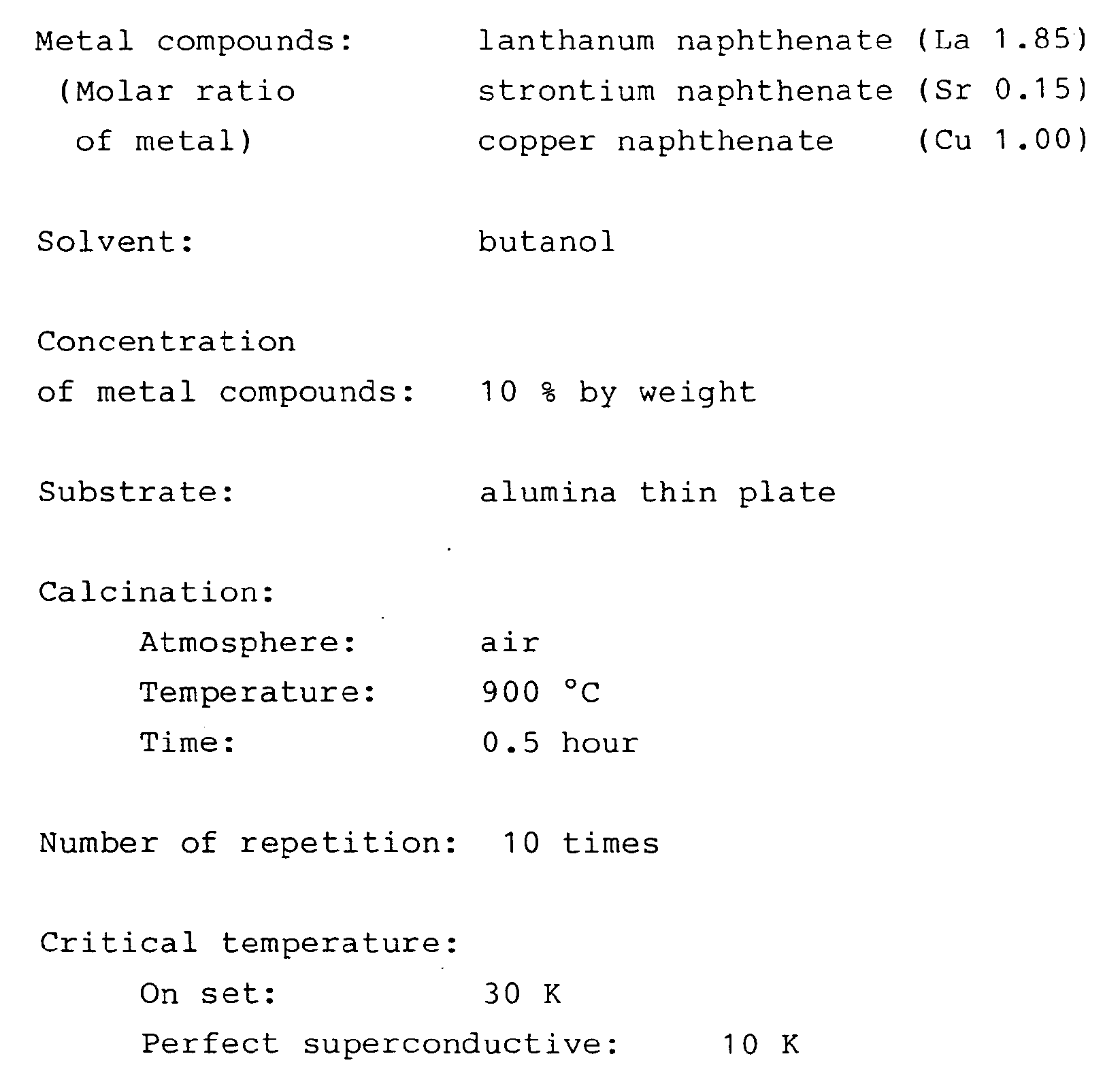
- The metal compounds shown above were mixed with each other and the mixture dissolved in the above solvent to give a coating solution having the total metal compounds concentration shown above and having the molar ratio of the metals as shown above. The coating solution was applied on the substrate shown above by immersing the substrate in the coating solution and the coat was dried in the air. Then the substrate having the dried coat was calcined under the conditions shown above. The immersing, drying and calcining steps were repeated 10 times to give a superconductive material whose electrical resistivity was abruptly decreased at the temperature (on set) shown above and which exhibited perfect superconductivity at the temperature shown above.
- The above procedure was repeated in the same manner as described using an alumina bar (diameter 1 mm) in place of the alumina plate as a substrate. The resultant superconductive composite materials showed similar critical temperature.
- The electrical conductivity was measured by the four termini method in which four spaced apart electrodes with about 2 mm distance were provided on the superconductive layer by coating a silver paste thereon.
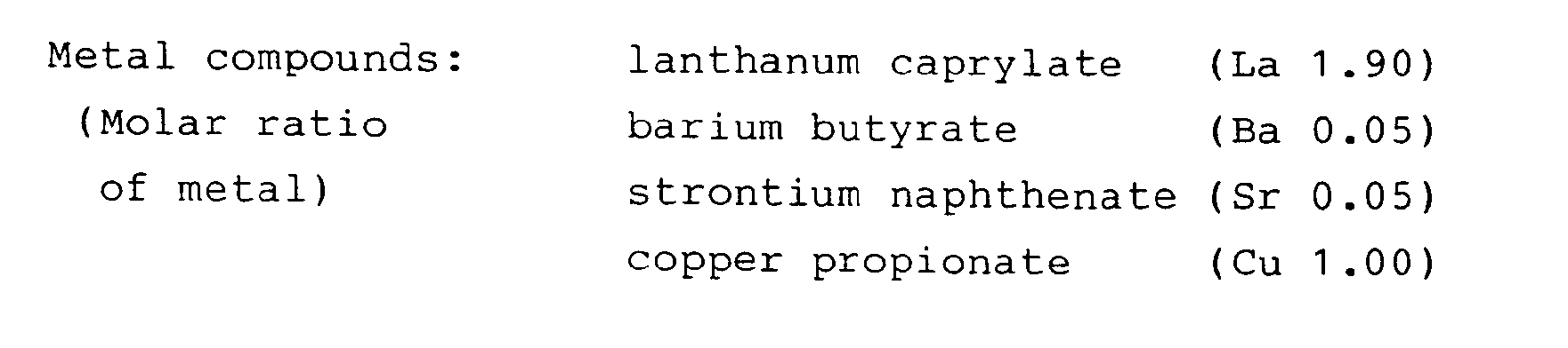
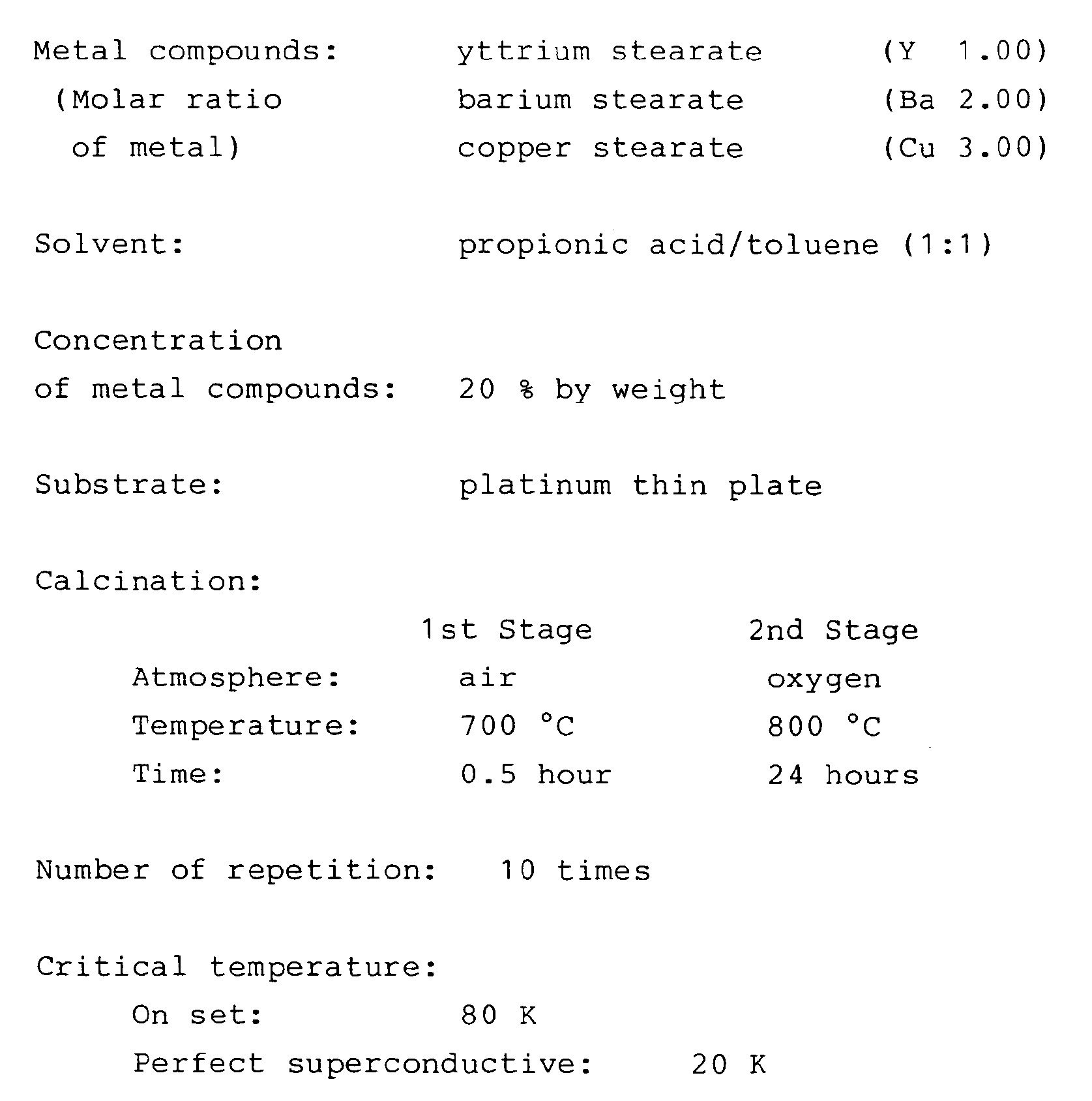
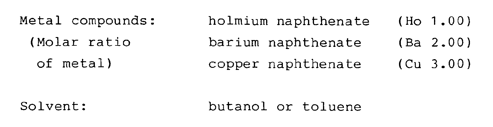
- Examples 2-17 were conducted to prepare various superconductive materials under conditions as summarized below. In each of Examples 2-17, the procedure including coating, drying and 1st stage calcination steps was repeated in the number indicated below. Thereafter, the 2nd stage calcination was performed in an oxygen-containing atmosphere. The calcined product was then gradually cooled to room temperature.
-

-

-


-


-


-

-


-


-
-

-


-

-

-


-

-

Claims (11)
- A method of preparing a superconductive material having a superconductive metal oxide layer provided on a substrate, said method comprising the steps of:(a) providing a non-aqueous solution containing a blend of metal compounds having a composition corresponding to that of the metals in the superconductive metal oxide, said metal compounds being selected from salts, chelates, halides, hydroxides, peroxides and oxides of said metals;(b) applying said solution on the substrate to form a liquid film;(c) drying said liquid film; and(d) calcining said dried film to convert said metal compounds into a superconductive metal oxide layer.
- A method as claimed in Claim 1, wherein said substrate is in the form of a wire or a plate.
- A method as claimed in Claim 1 or Claim 2, wherein said metal compounds are compounds capable of forming oxides upon calcination at 1000°C or less.
- A method as claimed in Claim 3, wherein said metal compounds are naphthenates, octylates, caprylates, stearates, laurates, butyrates, propionates, oxalates, citrates, lactates, benzoates, salcilates, ethylenediaminetetracetates, nitrates, carbonates, hydrochlorides or acetylacetonates of said metals.
- A method as claimed in Claim 3 or Claim 4, wherein step (d) is performed at a temperature of 500-1000°C.
- A method as claimed in Claim 5, wherein step (d) is performed in an oxygen-containing atmosphere for from 0.5 hour or more.
- A method as claimed in Claim 6, wherein the calcination in the oxygen-containing atmosphere is preceded by calcination in an oxygen-free atmosphere.
- A method as claimed in any preceding claim, wherein steps (a) to (d) are repeated until said superconductive layer has a thickness of 0.01-20 »m.
- A method as claimed in any preceding claim, wherein said solution contains a first compound selected from Y compounds, La compounds, Nd compounds, Sm compounds, Eu compounds, Gd compounds, Dy compounds, Ho compounds, Er compounds, Yb compounds, Lu compounds and mixtures thereof, a second compound selected from Ba compounds, Sr compounds, Ca compounds and mixtures thereof and a Cu compound so that said superconductive metal oxide has the formula:
AB₂Cu₃O7+x
wherein A stands for Y, La, Nd, Sm, Eu, Gd, Dy, Ho, Er, Yb, Lu, or a mixture of two or more thereof, B stands for Ba, Sr, Ca or a mixture of two or more thereof, and x stands for a number greater than -1 but less than +1. - A method as claimed in any one of Claims 1-8, wherein said solution contains a La compound, a compound selected from Ba compounds, Sr compounds, Ca compounds and mixtures thereof and a Cu compound, so that said superconductive metal oxide has the formula:
(La1-yZy)₂CuO4-z
wherein Z stands for Ba, Sr, Ca or a mixture of two or more thereof, y is greater than 0 but not greater than 0.2 and z is a number less than 1 but not less than 0. - A method as claimed in any preceding claim, wherein said substrate is formed of a metal, metal oxide or a ceramic.
Applications Claiming Priority (4)
| Application Number | Priority Date | Filing Date | Title |
|---|---|---|---|
| JP2112887 | 1987-01-30 | ||
| JP21128/87 | 1987-01-30 | ||
| JP11518687 | 1987-05-12 | ||
| JP115186/87 | 1987-05-12 |
Publications (3)
| Publication Number | Publication Date |
|---|---|
| EP0277020A2 EP0277020A2 (en) | 1988-08-03 |
| EP0277020A3 EP0277020A3 (en) | 1990-07-04 |
| EP0277020B1 true EP0277020B1 (en) | 1995-04-19 |
Family
ID=26358152
Family Applications (1)
| Application Number | Title | Priority Date | Filing Date |
|---|---|---|---|
| EP88300733A Expired - Lifetime EP0277020B1 (en) | 1987-01-30 | 1988-01-28 | Method of preparing a superconductive material |
Country Status (4)
| Country | Link |
|---|---|
| US (1) | US5039654A (en) |
| EP (1) | EP0277020B1 (en) |
| KR (1) | KR880009453A (en) |
| DE (1) | DE3853594T2 (en) |
Families Citing this family (21)
| Publication number | Priority date | Publication date | Assignee | Title |
|---|---|---|---|---|
| EP0287258B1 (en) * | 1987-04-10 | 1992-07-01 | AT&T Corp. | Method of producing a layer of superconductive material |
| AU607219B2 (en) * | 1987-05-29 | 1991-02-28 | Toray Industries, Inc. | Method of forming superconductive thin films and solutions for forming the same |
| US5304536A (en) * | 1987-06-09 | 1994-04-19 | E. I. Du Pont De Nemours And Company | Process for making superconductor powder |
| US4908346A (en) * | 1987-07-01 | 1990-03-13 | Eastman Kodak Company | Crystalline rare earth alkaline earth copper oxide thick film circuit element with superconducting onset transition temperature in excess of 77% |
| US5071830A (en) * | 1988-08-31 | 1991-12-10 | Superconductor Technologies, Inc. | Metalorganic deposition method for forming epitaxial thallium-based copper oxide superconducting films |
| ATE135134T1 (en) * | 1988-08-31 | 1996-03-15 | Superconductor Tech | SUPERCONDUCTING PRODUCT CONTAINING THALLIUM |
| JP3081212B2 (en) * | 1990-03-06 | 2000-08-28 | 日産自動車株式会社 | Synthesis method of composite oxide by partial citrate method |
| IT1248618B (en) * | 1990-08-01 | 1995-01-21 | Sviluppo Materiali Spa | DEVICE FOR THE CONTINUOUS PRODUCTION OF SUPERCONDUCTIVE CERAMICS |
| US5273776A (en) * | 1991-12-06 | 1993-12-28 | Mitsubishi Materials Corporation | Method for forming thermistor thin film |
| US6174564B1 (en) | 1991-12-13 | 2001-01-16 | Symetrix Corporation | Method of making metal polyoxyalkylated precursor solutions |
| DE4304679C2 (en) * | 1992-02-17 | 1996-03-21 | Mitsubishi Electric Corp | Process for producing a thin dielectric layer of an oxide system using the CVD process |
| JP2976028B1 (en) * | 1998-10-13 | 1999-11-10 | 工業技術院長 | Method for producing dense and epitaxial metal oxide film, precursor of metal oxide and method for producing the same |
| US6210752B1 (en) * | 1999-03-24 | 2001-04-03 | Sandia Corporation | All-alkoxide synthesis of strontium-containing metal oxides |
| JP2001279239A (en) * | 2000-03-29 | 2001-10-10 | Sumitomo Chem Co Ltd | Method for producing phosphor for light emitting element and phosphor paste |
| US20020056401A1 (en) * | 2000-10-23 | 2002-05-16 | Rupich Martin W. | Precursor solutions and methods of using same |
| JP4135857B2 (en) * | 2001-03-27 | 2008-08-20 | 独立行政法人産業技術総合研究所 | Infrared sensor manufacturing method |
| JP3548801B2 (en) * | 2001-03-27 | 2004-07-28 | 独立行政法人産業技術総合研究所 | A solution composition containing a metal complex in which a specific ligand is coordinated to a specific metal species, a solution composition for producing a rare-earth superconducting film, an amorphous solid of a specific metal complex, a specific coordination to a specific metal species A method for producing a solution containing a metal complex coordinated with an atom, a method for producing a solution for producing a rare earth superconducting film, and a method for forming a superconducting thin film. |
| JP4050730B2 (en) * | 2004-07-30 | 2008-02-20 | 株式会社東芝 | Oxide superconductor and manufacturing method thereof |
| JP4258536B2 (en) * | 2006-08-11 | 2009-04-30 | 独立行政法人産業技術総合研究所 | Method for producing crystallized metal oxide thin film |
| US20080044590A1 (en) * | 2006-08-21 | 2008-02-21 | National Institute Of Advanced Industrial Science And Technology | Manufacturing Method of Phosphor Film |
| JP5445982B2 (en) | 2009-12-09 | 2014-03-19 | 独立行政法人産業技術総合研究所 | Rare earth superconducting film forming solution and method for producing the same |
Citations (1)
| Publication number | Priority date | Publication date | Assignee | Title |
|---|---|---|---|---|
| US4485094A (en) * | 1983-01-28 | 1984-11-27 | Westinghouse Electric Corp. | Method of making ABO3 of the cubic perovskite structure |
Family Cites Families (8)
| Publication number | Priority date | Publication date | Assignee | Title |
|---|---|---|---|---|
| US3840389A (en) * | 1972-07-05 | 1974-10-08 | Gulf Research Development Co | Process for coating refractory oxides |
| US3865923A (en) * | 1973-03-19 | 1975-02-11 | Ethyl Corp | Catalyst |
| CA1077011A (en) * | 1975-04-08 | 1980-05-06 | Elrey L. Mccann (Iii) | Catalytic metal oxides on perovskite supports |
| JPS58156350A (en) * | 1982-03-12 | 1983-09-17 | Matsushita Electric Ind Co Ltd | Apparatus for purifying exhaust gas |
| JPS58174237A (en) * | 1982-04-02 | 1983-10-13 | Nissan Motor Co Ltd | Reforming catalyst of methanol |
| JPS59182283A (en) * | 1983-03-29 | 1984-10-17 | 株式会社東芝 | Manufacture of electroconductive ceramic sintered body |
| US4880770A (en) * | 1987-05-04 | 1989-11-14 | Eastman Kodak Company | Metalorganic deposition process for preparing superconducting oxide films |
| US4897378A (en) * | 1987-05-22 | 1990-01-30 | Massachusetts Institute Of Technology | Preparation of thin film superconducting oxides |
-
1988
- 1988-01-28 EP EP88300733A patent/EP0277020B1/en not_active Expired - Lifetime
- 1988-01-28 DE DE3853594T patent/DE3853594T2/en not_active Expired - Fee Related
- 1988-01-28 KR KR1019880000708A patent/KR880009453A/en not_active Withdrawn
-
1989
- 1989-06-30 US US07/373,599 patent/US5039654A/en not_active Expired - Fee Related
Patent Citations (1)
| Publication number | Priority date | Publication date | Assignee | Title |
|---|---|---|---|---|
| US4485094A (en) * | 1983-01-28 | 1984-11-27 | Westinghouse Electric Corp. | Method of making ABO3 of the cubic perovskite structure |
Non-Patent Citations (5)
| Title |
|---|
| APPLIED PHYSICS LETTERS, vol. 51, no. 22, 30 December 1987, New York, US, pp. 1842-1844 ; C. E. RICE et al: "Preparation of superconducting thin films of Ba2YCu307 by a novel spin-on pyrolysis technique" * |
| APPLIED PHYSICS LETTERS, vol. 51, no. 25, 21 December 1987, New York, US, pp. 2152-2154 ; A. H. HAMDI et al: "Formation of thin-film high Tc superconductors by metalorganic deposition" * |
| PHYS. REV. LETT., Vol. 58, No. 4, 26 January 1987, pp. 405-407, C. W. Chu et al. * |
| PRAMANA-J. PHYS., Vol. 28, No. 3, March 1987, pp. L321-L323, P. Ganguly et al. * |
| Z. PHYS. B, Condensed Matter 64, (1986), pp. 189-193, J. G. Bednorz and K. A. Müller * |
Also Published As
| Publication number | Publication date |
|---|---|
| KR880009453A (en) | 1988-09-15 |
| DE3853594T2 (en) | 1995-08-31 |
| EP0277020A2 (en) | 1988-08-03 |
| DE3853594D1 (en) | 1995-05-24 |
| US5039654A (en) | 1991-08-13 |
| EP0277020A3 (en) | 1990-07-04 |
Similar Documents
| Publication | Publication Date | Title |
|---|---|---|
| US5039654A (en) | Superconductive material and method of preparing same | |
| JP5014131B2 (en) | Method for producing highly organized tape-like high-temperature superconductor | |
| US4959347A (en) | Forming homogeneous precursers of Bi-Sr-Ca-Cu via carboxylates in the presence of oxidizing agents | |
| JP4592696B2 (en) | Method for producing precursor solution for metalorganic vapor deposition using superconducting oxide and method for producing thin film superconductor by metalorganic vapor deposition | |
| JP4203606B2 (en) | Oxide superconducting thick film composition and thick film tape-shaped oxide superconductor | |
| JPH059022A (en) | Production of superconductor | |
| JPH07106905B2 (en) | Method for manufacturing superconductor and superconductor | |
| JPH0476324B2 (en) | ||
| JPH0476323B2 (en) | ||
| JP2916615B2 (en) | Method for producing composite metal oxide epitaxial film having perovskite structure | |
| KR100807640B1 (en) | Precursor solution to form biaxially oriented buffer layer by low temperature heat treatment | |
| US6559103B1 (en) | Method for producing superconducting oxide compounds | |
| KR100998310B1 (en) | Method for forming precursor solution for organometallic deposition and method for forming superconducting thick film using same | |
| Celik et al. | High voltage breakdown capabilities of high temperature insulation coatings for HTS and LTS conductors | |
| JPH0562545A (en) | Oxide type superconductor and its manufacture | |
| JPS63276820A (en) | Manufacture of oxide superconductor | |
| Grader et al. | Forming methods for high Tc superconductors | |
| JPH01151111A (en) | Manufacture of oxide system superconductive film | |
| JPH0198277A (en) | Method for forming superconductor thin films | |
| JPH03102715A (en) | Superconductive ceramics wire material and manufacture thereof | |
| JPH01166416A (en) | Manufacture of oxide superconductive wire material | |
| JPH0360458A (en) | Production of oxide superconductor | |
| JPS63279529A (en) | Manufacture of superconductor molding | |
| JPH01198485A (en) | Production of body coated with compound metal oxide having specified composition | |
| CN105683126A (en) | Precursor composition for alkaline earth metal containing ceramic layers |
Legal Events
| Date | Code | Title | Description |
|---|---|---|---|
| PUAI | Public reference made under article 153(3) epc to a published international application that has entered the european phase |
Free format text: ORIGINAL CODE: 0009012 |
|
| AK | Designated contracting states |
Kind code of ref document: A2 Designated state(s): CH DE FR GB LI |
|
| PUAL | Search report despatched |
Free format text: ORIGINAL CODE: 0009013 |
|
| AK | Designated contracting states |
Kind code of ref document: A3 Designated state(s): CH DE FR GB LI |
|
| 17P | Request for examination filed |
Effective date: 19901204 |
|
| 17Q | First examination report despatched |
Effective date: 19930623 |
|
| GRAA | (expected) grant |
Free format text: ORIGINAL CODE: 0009210 |
|
| AK | Designated contracting states |
Kind code of ref document: B1 Designated state(s): CH DE FR GB LI |
|
| REF | Corresponds to: |
Ref document number: 3853594 Country of ref document: DE Date of ref document: 19950524 |
|
| ET | Fr: translation filed | ||
| PLBE | No opposition filed within time limit |
Free format text: ORIGINAL CODE: 0009261 |
|
| STAA | Information on the status of an ep patent application or granted ep patent |
Free format text: STATUS: NO OPPOSITION FILED WITHIN TIME LIMIT |
|
| 26N | No opposition filed | ||
| PGFP | Annual fee paid to national office [announced via postgrant information from national office to epo] |
Ref country code: FR Payment date: 19980109 Year of fee payment: 11 |
|
| PGFP | Annual fee paid to national office [announced via postgrant information from national office to epo] |
Ref country code: GB Payment date: 19980119 Year of fee payment: 11 |
|
| PGFP | Annual fee paid to national office [announced via postgrant information from national office to epo] |
Ref country code: CH Payment date: 19980205 Year of fee payment: 11 |
|
| PGFP | Annual fee paid to national office [announced via postgrant information from national office to epo] |
Ref country code: DE Payment date: 19980206 Year of fee payment: 11 |
|
| PG25 | Lapsed in a contracting state [announced via postgrant information from national office to epo] |
Ref country code: GB Free format text: LAPSE BECAUSE OF NON-PAYMENT OF DUE FEES Effective date: 19990128 |
|
| PG25 | Lapsed in a contracting state [announced via postgrant information from national office to epo] |
Ref country code: LI Free format text: LAPSE BECAUSE OF NON-PAYMENT OF DUE FEES Effective date: 19990131 Ref country code: CH Free format text: LAPSE BECAUSE OF NON-PAYMENT OF DUE FEES Effective date: 19990131 |
|
| GBPC | Gb: european patent ceased through non-payment of renewal fee |
Effective date: 19990128 |
|
| REG | Reference to a national code |
Ref country code: CH Ref legal event code: PL |
|
| PG25 | Lapsed in a contracting state [announced via postgrant information from national office to epo] |
Ref country code: FR Free format text: LAPSE BECAUSE OF NON-PAYMENT OF DUE FEES Effective date: 19990930 |
|
| PG25 | Lapsed in a contracting state [announced via postgrant information from national office to epo] |
Ref country code: DE Free format text: LAPSE BECAUSE OF NON-PAYMENT OF DUE FEES Effective date: 19991103 |
|
| REG | Reference to a national code |
Ref country code: FR Ref legal event code: ST |