EP0275294B1 - Imaging lens array and optical print head - Google Patents
Imaging lens array and optical print head Download PDFInfo
- Publication number
- EP0275294B1 EP0275294B1 EP87905031A EP87905031A EP0275294B1 EP 0275294 B1 EP0275294 B1 EP 0275294B1 EP 87905031 A EP87905031 A EP 87905031A EP 87905031 A EP87905031 A EP 87905031A EP 0275294 B1 EP0275294 B1 EP 0275294B1
- Authority
- EP
- European Patent Office
- Prior art keywords
- print head
- lens array
- photosensitive surface
- imaging lens
- array
- Prior art date
- Legal status (The legal status is an assumption and is not a legal conclusion. Google has not performed a legal analysis and makes no representation as to the accuracy of the status listed.)
- Expired
Links
- 238000003384 imaging method Methods 0.000 title claims abstract description 37
- 230000003287 optical effect Effects 0.000 title abstract description 8
- 239000013307 optical fiber Substances 0.000 claims abstract description 18
- 238000003491 array Methods 0.000 claims description 6
- 230000000284 resting effect Effects 0.000 claims 1
- 239000003351 stiffener Substances 0.000 description 6
- 238000000429 assembly Methods 0.000 description 3
- 238000000034 method Methods 0.000 description 3
- 238000012546 transfer Methods 0.000 description 3
- 230000000712 assembly Effects 0.000 description 2
- 238000013461 design Methods 0.000 description 2
- 239000000835 fiber Substances 0.000 description 2
- 238000012360 testing method Methods 0.000 description 2
- 229910000831 Steel Inorganic materials 0.000 description 1
- 238000005452 bending Methods 0.000 description 1
- 230000008602 contraction Effects 0.000 description 1
- 238000001816 cooling Methods 0.000 description 1
- 238000011161 development Methods 0.000 description 1
- 230000008030 elimination Effects 0.000 description 1
- 238000003379 elimination reaction Methods 0.000 description 1
- 238000004519 manufacturing process Methods 0.000 description 1
- 239000002245 particle Substances 0.000 description 1
- 230000002093 peripheral effect Effects 0.000 description 1
- 238000012545 processing Methods 0.000 description 1
- 239000010959 steel Substances 0.000 description 1
Images


Classifications
-
- G—PHYSICS
- G03—PHOTOGRAPHY; CINEMATOGRAPHY; ANALOGOUS TECHNIQUES USING WAVES OTHER THAN OPTICAL WAVES; ELECTROGRAPHY; HOLOGRAPHY
- G03B—APPARATUS OR ARRANGEMENTS FOR TAKING PHOTOGRAPHS OR FOR PROJECTING OR VIEWING THEM; APPARATUS OR ARRANGEMENTS EMPLOYING ANALOGOUS TECHNIQUES USING WAVES OTHER THAN OPTICAL WAVES; ACCESSORIES THEREFOR
- G03B27/00—Photographic printing apparatus
- G03B27/32—Projection printing apparatus, e.g. enlarger, copying camera
- G03B27/52—Details
- G03B27/522—Projection optics
- G03B27/525—Projection optics for slit exposure
- G03B27/528—Projection optics for slit exposure in which the projection optics remain stationary
-
- B—PERFORMING OPERATIONS; TRANSPORTING
- B41—PRINTING; LINING MACHINES; TYPEWRITERS; STAMPS
- B41J—TYPEWRITERS; SELECTIVE PRINTING MECHANISMS, i.e. MECHANISMS PRINTING OTHERWISE THAN FROM A FORME; CORRECTION OF TYPOGRAPHICAL ERRORS
- B41J2/00—Typewriters or selective printing mechanisms characterised by the printing or marking process for which they are designed
- B41J2/435—Typewriters or selective printing mechanisms characterised by the printing or marking process for which they are designed characterised by selective application of radiation to a printing material or impression-transfer material
- B41J2/447—Typewriters or selective printing mechanisms characterised by the printing or marking process for which they are designed characterised by selective application of radiation to a printing material or impression-transfer material using arrays of radiation sources
- B41J2/45—Typewriters or selective printing mechanisms characterised by the printing or marking process for which they are designed characterised by selective application of radiation to a printing material or impression-transfer material using arrays of radiation sources using light-emitting diode [LED] or laser arrays
- B41J2/451—Special optical means therefor, e.g. lenses, mirrors, focusing means
-
- B—PERFORMING OPERATIONS; TRANSPORTING
- B41—PRINTING; LINING MACHINES; TYPEWRITERS; STAMPS
- B41J—TYPEWRITERS; SELECTIVE PRINTING MECHANISMS, i.e. MECHANISMS PRINTING OTHERWISE THAN FROM A FORME; CORRECTION OF TYPOGRAPHICAL ERRORS
- B41J2/00—Typewriters or selective printing mechanisms characterised by the printing or marking process for which they are designed
- B41J2/435—Typewriters or selective printing mechanisms characterised by the printing or marking process for which they are designed characterised by selective application of radiation to a printing material or impression-transfer material
- B41J2/447—Typewriters or selective printing mechanisms characterised by the printing or marking process for which they are designed characterised by selective application of radiation to a printing material or impression-transfer material using arrays of radiation sources
- B41J2/46—Typewriters or selective printing mechanisms characterised by the printing or marking process for which they are designed characterised by selective application of radiation to a printing material or impression-transfer material using arrays of radiation sources characterised by using glass fibres
-
- G—PHYSICS
- G03—PHOTOGRAPHY; CINEMATOGRAPHY; ANALOGOUS TECHNIQUES USING WAVES OTHER THAN OPTICAL WAVES; ELECTROGRAPHY; HOLOGRAPHY
- G03G—ELECTROGRAPHY; ELECTROPHOTOGRAPHY; MAGNETOGRAPHY
- G03G15/00—Apparatus for electrographic processes using a charge pattern
- G03G15/04—Apparatus for electrographic processes using a charge pattern for exposing, i.e. imagewise exposure by optically projecting the original image on a photoconductive recording material
- G03G15/04036—Details of illuminating systems, e.g. lamps, reflectors
- G03G15/04045—Details of illuminating systems, e.g. lamps, reflectors for exposing image information provided otherwise than by directly projecting the original image onto the photoconductive recording material, e.g. digital copiers
- G03G15/04054—Details of illuminating systems, e.g. lamps, reflectors for exposing image information provided otherwise than by directly projecting the original image onto the photoconductive recording material, e.g. digital copiers by LED arrays
-
- G—PHYSICS
- G03—PHOTOGRAPHY; CINEMATOGRAPHY; ANALOGOUS TECHNIQUES USING WAVES OTHER THAN OPTICAL WAVES; ELECTROGRAPHY; HOLOGRAPHY
- G03G—ELECTROGRAPHY; ELECTROPHOTOGRAPHY; MAGNETOGRAPHY
- G03G15/00—Apparatus for electrographic processes using a charge pattern
- G03G15/22—Apparatus for electrographic processes using a charge pattern involving the combination of more than one step according to groups G03G13/02 - G03G13/20
- G03G15/32—Apparatus for electrographic processes using a charge pattern involving the combination of more than one step according to groups G03G13/02 - G03G13/20 in which the charge pattern is formed dotwise, e.g. by a thermal head
- G03G15/326—Apparatus for electrographic processes using a charge pattern involving the combination of more than one step according to groups G03G13/02 - G03G13/20 in which the charge pattern is formed dotwise, e.g. by a thermal head by application of light, e.g. using a LED array
-
- G—PHYSICS
- G03—PHOTOGRAPHY; CINEMATOGRAPHY; ANALOGOUS TECHNIQUES USING WAVES OTHER THAN OPTICAL WAVES; ELECTROGRAPHY; HOLOGRAPHY
- G03G—ELECTROGRAPHY; ELECTROPHOTOGRAPHY; MAGNETOGRAPHY
- G03G15/00—Apparatus for electrographic processes using a charge pattern
- G03G15/04—Apparatus for electrographic processes using a charge pattern for exposing, i.e. imagewise exposure by optically projecting the original image on a photoconductive recording material
- G03G15/043—Apparatus for electrographic processes using a charge pattern for exposing, i.e. imagewise exposure by optically projecting the original image on a photoconductive recording material with means for controlling illumination or exposure
- G03G15/0435—Apparatus for electrographic processes using a charge pattern for exposing, i.e. imagewise exposure by optically projecting the original image on a photoconductive recording material with means for controlling illumination or exposure by introducing an optical element in the optical path, e.g. a filter
Definitions
- the present invention relates to optical print heads and to means for transmitting light emitted from the print heads to a photosensitive surface, and more particularly to means for accurately spacing (1) the print head from the photosensitive surface and (2) the transmitting means from the print head to maintain high resolution and good exposure uniformity.
- High speed optical printing devices used in data processing systems are intended for converting electric input signals into printed form, and include photosensitive means and light sources such as linear arrays of light emitting diodes (LED's), photodiodes, or similar devices.
- Light from a source is often transmitted to the photosensitive means via a plurality of gradient index optical fibers forming an imaging lens array.
- imaging lens arrays are commercially available as SELFOC (a trademark of Nippon Sheet Glass Co., Ltd.) lenses in a staggered, two-row bundle of optical fibers as described in U.S. Patent 3,658,407, patented on April 25, 1972. Reference may be made to that patent for details of the lens arrays.
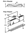
- a gradient index optical fiber 10 is illustrated in Fig. 1.
- the refractive index distribution of the optical fiber varies parabolically outwards from the longitudinal axis of the optical fiber towards the peripheral portion thereof.
- Fig. 2 shows an imaging lens array 12 formed of a staggered, two-row bundle of optical fibers 10. If the distances L1 and L2 are properly selected and equal, then there is obtained an erect image at a magnification of one of an object.
- Imaging lens arrays such as shown in Fig. 2 have been proposed for transmitting light between an array of LED's 14 and photosensitive means such as a photoconductive member 16.
- dimensions L TC , L1, and L2 must be accurately set and maintained.
- the total conjugate L TC does not vary from lens to lens and that, as such, the spacing between the object plane and the image plane can be fixed at the total conjugate distance. While this approximation is adequate for low resolution applications, in fact however, the lens parameters L TC and L F vary considerably between manufacturers, and even between lenses of the same manufacturer.
- an object of the present invention to provide means for locating an imaging lens array on a print head and for locating the print head relative to photosensitive means at the image plane in a way which allows for convenient and accurate compensation for variations in lens dimensions.
- Several significant benefits are provided by the locating means to be described. These benefits stem from the precise locational and adjustment capabilities built into the locating means, and include (1) low parts cost due to relaxed tolerances, (2) elimination in most instances of adjustments of the locating means at the machine level, both in final in-plant assembly and in the field because such adjustments have been affected during sub-assembly of the lens array to the print head, and (3) ability to perform direct, in-the-field replacement due to the interchangeability of print head and lens array sub-assemblies.
- novel apparatus for locating an imaging lens array formed of a plurality of gradient index optical fibers on a print head having a linear array of light sources, such that (1) the light sources are readily spaced from a photosensitive surface a distance equal to the total conjugate of the imaging lens array, and (2) the optical fibers are accurately spaced from the light sources in a direction along their optical axes so as to be midway between the light sources and the photosensitive surface.
- locating means are provided for removably supporting the print head relative to the photosensitive surface such that the light sources of the print head are spaced from the photosensitive surface by the total conjugate of the optical fibers.
- Mounting means support the lens array to the print head so as to center the lens array between the light sources and the photosensitive surface.
- electrophotographic apparatus generally designated 18 includes a charging station 20 for applying a uniform charge to photosensitive means such as a photoconductor 22.
- the photoconductor illustrated is an endless belt trained about a plurality of rollers and driven in the direction of an arrow 24.
- Light from selected LED's of a print head 26 is transmitted by an imaging lens array 28 onto the surface of photoconductor 22 as the photoconductor passes over a roller 29.
- the light striking the charged photoconductor selectively dissipates portions of the charge to form an electrostatic latent image on the photoconductor. Selection of the specific LED's of the print head which are activated at any given time is by means of writer control electronics 30, a logic and control unit 32, and the data entering along line 34.
- a magnetic brush development station 36 transfers toner particles to the photoconductor for developing the latent image.
- the resulting toned image then travels to a transfer and detack station 38 where the image is transferred to a copy sheet fed from a supply, not shown, along path 40. After the photoconductor passes through transfer and detack, it is cleaned at station 42 and is available for another cycle of operation.
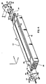
- a sub-assembly 44 includes the print head 26 and imaging lens array 28, both of which are schematically shown in Fig. 3.
- the print head per se is a conventional, commercially-available unit with a linear array of LED's, a transparent faceplate covering the LED's, and heat-conducting cooling vanes 46.
- Imaging lens array 28 includes a staggered, two-row bundle of gradient index optical fibers disposed above the LED array of the print head. The ends of the optical fibers are accurately spaced in a Z-direction (along the optical axes of the fibers) from the LED's by a distance L1 as shown in Fig.
- the lens array is preferably longer than the LED array so that the position of the imaging lens array along the X-direction (along the length of the LED array) is not as critical.
- imaging lens array 28 has been bonded between two stiffeners 48 and 50.
- Stiffener 48 has a pair of arms 52 and 54 for attaching the stiffener (and thereby the imaging lens) to the print head.
- An interface block 56 is slidably mounted on print head 26 by a pair of screws 58 and 60 and elongated holes in the block through which the screws pass.
- block 56 is slid (the screws being loose) until an upstanding wing 62 abuts arm 52 of stiffener 48. Screws 58 and 60 are tightened.
- a set screw 64 is tightened to totally constrain arm 52 relative to the print head.
- the attachment means for arm 54 can best be seen in Figs. 7 and 8 (as well as Fig. 4.
- the coefficient of thermal expansion of the imaging lens array and stiffeners may differ from that of the print head, and must be accounted for in the design of the mounting means.
- the attachment of arm 54 is not the same as that of arm 52 and provides for such thermal expansion.
- An interface block 66 is slidably mounted in the Y-direction on print head 26 by a pair of screws 68 and 70 which pass through respective elongated holes in block 66.
- a flexible steel plate 72 is mounted at its ends to block 66 by a pair of screws 74 and 76 which also pass through elongated holes to permit vertical (Z-direction) movement of the plate relative to the interface block.
- interface block 66 and plate 72 thereon are moved relative to arm 54 until a screw hole in the plate aligns with a predrilled and tapped hole in the end of arm 54.
- a screw 78 is inserted into the tapped hole and screws 68, 70, 74, 76 and 78 are tightened to secure the sub-assembly elements such that movement of imaging lens array 28 in directions along its optical axis (Z-direction) and lateral to the LED array (Y-direction) is inhibited, while thermal expansion and contraction of the imaging lens array and stiffeners along their lengths (X-direction) at a rate different than expansion of the print head is permitted.
- mounting means are provided for the imaging lens to maintain critical spacing between the print head LED array and the imaging lens array equal to distance L2.
- Critical adjustments can be easily and rapidly made during assembly without the need for high precision parts.
- print head sub-assembly 44 must be mounted on electrophotographic apparatus 18 such that the LED array is spaced from the surface of photoconductor 22 by a distance L TC equal to the total conjugate of imaging lens array 28, and the imaging lens array itself must be spaced by distance L2 from the photoconductor.
- adjustable mounting means have been provided, whereby the distance between the LED array of print head 26 and the surface of photoconductor 22 can be adjusted to match the total conjugate distance L TC of the specific imaging lens array attached to the print head.
- the locating structures include a V-shaped opening 80 in a plate 82, and a pair of pins 84 and 86 which extend from a mechanism plate (not shown) in the electrophotographic apparatus. Opening 80 and pins 84 and 86 are fixed in the electrographic apparatus mainframe at accurately known positions relative to the bearings of roller 29. This spacial relationship is intended to be substantially invariant from machine to machine so that once set up, a print head assembly 44 can be mounted on any apparatus, in most instances, without further adjustment in the field.
- Bracket 90 includes a pin 92 and a pair of elongated slots through which the plate can be screwed to interface block 56.
- Second bracket 94 has holes 96 and 98 and a pair of elongated slots through which the second plate can be screwed to interface block 66. Holes 89 and 91 in plate 82 and bracket 94 are provided for the bearings of roller 29.
- the mounting brackets can be used to attach print head assembly 44 to the electrographic apparatus mainframe.
- Pin 92 extends through V-shaped opening 80 in plate 82 and defines a reference surface which rests against the bottom of the hole.
- Pin 84 of the electrophotographic apparatus mainframe extends through hole 96, whose reference surfaces rest on the pin.
- Pin 86 extends through hole 98 to inhibit rotation of bracket 94 about pin 84, thereby totally constraining the print head assembly.
- the positions of the brackets are adjusted such that the stand-off of the LED array to the photoconductor is equal to the total conjugate of the imaging lens array.
- the determination of the stand-off dimension is not a part of the present invention, and various methods are available. For example, a trial and error method can be used wherein test prints are made until satisfactory print quality is obtained.
- published Japanese patent application No. 58-146832 describes a system wherein such test printing is made unnecessary by placing an array of photodetectors at the image plane and adjusting the position of the optical system in accordance with the detected value.
- brackets 90 and 94 are tightig screwed to print head 26.
- print head assembly 44 is readily removable from the electrophotographic apparatus and will have exact locational repeatability upon reinstallation. Since the reference surfaces of V-shaped opening 80 and pins 84 and 86 can be fixed accurately in every electrophotographic apparatus at time of manufacture, field replacement of print head assemblies can be effected without adjustment. Interchangeability of print head assemblies is assured.
Landscapes
- Physics & Mathematics (AREA)
- Optics & Photonics (AREA)
- General Physics & Mathematics (AREA)
- Health & Medical Sciences (AREA)
- General Health & Medical Sciences (AREA)
- Toxicology (AREA)
- Printers Or Recording Devices Using Electromagnetic And Radiation Means (AREA)
- Dot-Matrix Printers And Others (AREA)
- Fax Reproducing Arrangements (AREA)
Abstract
Description
- The present invention relates to optical print heads and to means for transmitting light emitted from the print heads to a photosensitive surface, and more particularly to means for accurately spacing (1) the print head from the photosensitive surface and (2) the transmitting means from the print head to maintain high resolution and good exposure uniformity.
- High speed optical printing devices used in data processing systems are intended for converting electric input signals into printed form, and include photosensitive means and light sources such as linear arrays of light emitting diodes (LED's), photodiodes, or similar devices. Light from a source is often transmitted to the photosensitive means via a plurality of gradient index optical fibers forming an imaging lens array. Such imaging lens arrays are commercially available as SELFOC (a trademark of Nippon Sheet Glass Co., Ltd.) lenses in a staggered, two-row bundle of optical fibers as described in U.S. Patent 3,658,407, patented on April 25, 1972. Reference may be made to that patent for details of the lens arrays.
- A gradient index
optical fiber 10 is illustrated in Fig. 1. The refractive index distribution of the optical fiber varies parabolically outwards from the longitudinal axis of the optical fiber towards the peripheral portion thereof. - Fig. 2 shows an
imaging lens array 12 formed of a staggered, two-row bundle ofoptical fibers 10. If the distances L₁ and L₂ are properly selected and equal, then there is obtained an erect image at a magnification of one of an object. Distance LTC represents the total conjugate of the lens (i.e., the distance between the object and image planes). Accordingly:

optical fibers 10 ofimaging lens array 12. - Imaging lens arrays such as shown in Fig. 2 have been proposed for transmitting light between an array of LED's 14 and photosensitive means such as a
photoconductive member 16. For optimum resolution, dimensions LTC , L₁, and L₂ must be accurately set and maintained. In the design of prior art devices such as shown in U.S. Patent No. 4,147,412, it is assumed that the total conjugate LTC does not vary from lens to lens and that, as such, the spacing between the object plane and the image plane can be fixed at the total conjugate distance. While this approximation is adequate for low resolution applications, in fact however, the lens parameters LTC and LF vary considerably between manufacturers, and even between lenses of the same manufacturer. - It is, therefore, an object of the present invention to provide means for locating an imaging lens array on a print head and for locating the print head relative to photosensitive means at the image plane in a way which allows for convenient and accurate compensation for variations in lens dimensions. Several significant benefits are provided by the locating means to be described. These benefits stem from the precise locational and adjustment capabilities built into the locating means, and include (1) low parts cost due to relaxed tolerances, (2) elimination in most instances of adjustments of the locating means at the machine level, both in final in-plant assembly and in the field because such adjustments have been affected during sub-assembly of the lens array to the print head, and (3) ability to perform direct, in-the-field replacement due to the interchangeability of print head and lens array sub-assemblies.
- In accordance with the present invention as claimed, novel apparatus is provided for locating an imaging lens array formed of a plurality of gradient index optical fibers on a print head having a linear array of light sources, such that (1) the light sources are readily spaced from a photosensitive surface a distance equal to the total conjugate of the imaging lens array, and (2) the optical fibers are accurately spaced from the light sources in a direction along their optical axes so as to be midway between the light sources and the photosensitive surface.
- In a preferred embodiment of the present invention, locating means are provided for removably supporting the print head relative to the photosensitive surface such that the light sources of the print head are spaced from the photosensitive surface by the total conjugate of the optical fibers. Mounting means support the lens array to the print head so as to center the lens array between the light sources and the photosensitive surface.
- The invention, and its objects and advantages, will become more apparent in the detailed description of the preferred embodiment presented below.
- In the detailed description of the preferred embodiment of the invention presented below, reference is made to the accompanying drawings in which:
- Fig. 1 is a representation of an optical fiber in accordance with the prior art and wherein the geometry of the fiber is illustrated;
- Fig. 2 is a perspective view of an imaging lens array formed by a staggered, two-row bundle of optical fibers as shown in Fig. 1, and also shows a print head with an LED array at the object plane and photosensitive means at the image plane;
- Fig. 3 is a schematic vertical section of an electrophotographic apparatus including the imaging lens array and print head of Fig. 2;
- Fig. 4 is a perspective view of a print head and imaging lens array sub-assembly with locating means in accordance with the present invention;
- Figs. 5 and 6 are top and side views, respectively, showing details of a portion of the locating means; and
- Figs. 7 and 8 are top and side views, respectively, showing details of another portion of the locating means.
- The present description will be directed in particular to elements forming part of, or cooperating more directly with, apparatus in accordance with the present invention. It is to be understood that elements, components, and/or sub components not specifically shown or described may take various forms well known to those skilled in the art.
- To assist in understanding the present invention, an electrophotographic copier/printer in which the invention may be used will be briefly described. It will be understood, however, that the apparatus of the present invention can be used in other types of apparatus.
- Referring to Fig. 3, electrophotographic apparatus generally designated 18 includes a
charging station 20 for applying a uniform charge to photosensitive means such as aphotoconductor 22. The photoconductor illustrated is an endless belt trained about a plurality of rollers and driven in the direction of anarrow 24. Light from selected LED's of aprint head 26 is transmitted by animaging lens array 28 onto the surface ofphotoconductor 22 as the photoconductor passes over aroller 29. The light striking the charged photoconductor selectively dissipates portions of the charge to form an electrostatic latent image on the photoconductor. Selection of the specific LED's of the print head which are activated at any given time is by means ofwriter control electronics 30, a logic andcontrol unit 32, and the data entering alongline 34. - A magnetic
brush development station 36 transfers toner particles to the photoconductor for developing the latent image. The resulting toned image then travels to a transfer anddetack station 38 where the image is transferred to a copy sheet fed from a supply, not shown, alongpath 40. After the photoconductor passes through transfer and detack, it is cleaned atstation 42 and is available for another cycle of operation. - Referring to Fig. 4, a
sub-assembly 44 includes theprint head 26 andimaging lens array 28, both of which are schematically shown in Fig. 3. The print head per se is a conventional, commercially-available unit with a linear array of LED's, a transparent faceplate covering the LED's, and heat-conductingcooling vanes 46.Imaging lens array 28 includes a staggered, two-row bundle of gradient index optical fibers disposed above the LED array of the print head. The ends of the optical fibers are accurately spaced in a Z-direction (along the optical axes of the fibers) from the LED's by a distance L₁ as shown in Fig. 2 as well as being accurately positioned in a Y-direction (lateral to the LED array) so as to align with the LED's along the length of the print head. The lens array is preferably longer than the LED array so that the position of the imaging lens array along the X-direction (along the length of the LED array) is not as critical. - Commercially available imaging lens arrays of the type discussed herein are somewhat flexible and tend to bend. It will be appreciated that very little bending would be needed to cause significant defocusing of the image of the LED's on the photoconductor. Accordingly,
imaging lens array 28 has been bonded between twostiffeners arms - Details of the attachment means for
arm 52 are better seen in Figs. 5 and 6. Aninterface block 56 is slidably mounted onprint head 26 by a pair ofscrews imaging lens array 28 has been properly aligned laterally with the LED array (the Y-direction of Fig. 4),block 56 is slid (the screws being loose) until anupstanding wing 62abuts arm 52 ofstiffener 48.Screws set screw 64 is tightened to totally constrainarm 52 relative to the print head. - The attachment means for
arm 54 can best be seen in Figs. 7 and 8 (as well as Fig. 4. The coefficient of thermal expansion of the imaging lens array and stiffeners may differ from that of the print head, and must be accounted for in the design of the mounting means. The attachment ofarm 54 is not the same as that ofarm 52 and provides for such thermal expansion. Afterimaging lens array 28 has been properly aligned with and spaced from the LED array, as described above, final attachment ofarm 54 can be effected. Aninterface block 66 is slidably mounted in the Y-direction onprint head 26 by a pair ofscrews block 66. Aflexible steel plate 72 is mounted at its ends to block 66 by a pair ofscrews - During assembly,
interface block 66 andplate 72 thereon are moved relative toarm 54 until a screw hole in the plate aligns with a predrilled and tapped hole in the end ofarm 54. Ascrew 78 is inserted into the tapped hole and screws 68, 70, 74, 76 and 78 are tightened to secure the sub-assembly elements such that movement ofimaging lens array 28 in directions along its optical axis (Z-direction) and lateral to the LED array (Y-direction) is inhibited, while thermal expansion and contraction of the imaging lens array and stiffeners along their lengths (X-direction) at a rate different than expansion of the print head is permitted. - By the apparatus described, mounting means are provided for the imaging lens to maintain critical spacing between the print head LED array and the imaging lens array equal to distance L₂. Critical adjustments can be easily and rapidly made during assembly without the need for high precision parts. However, for optimum resolution and exposure uniformity,
print head sub-assembly 44 must be mounted onelectrophotographic apparatus 18 such that the LED array is spaced from the surface ofphotoconductor 22 by a distance LTC equal to the total conjugate ofimaging lens array 28, and the imaging lens array itself must be spaced by distance L₂ from the photoconductor. To that end, adjustable mounting means have been provided, whereby the distance between the LED array ofprint head 26 and the surface ofphotoconductor 22 can be adjusted to match the total conjugate distance LTC of the specific imaging lens array attached to the print head. - Three locating structures are provided on the electrographic apparatus. The locating structures include a V-shaped
opening 80 in aplate 82, and a pair ofpins 84 and 86 which extend from a mechanism plate (not shown) in the electrophotographic apparatus.Opening 80 and pins 84 and 86 are fixed in the electrographic apparatus mainframe at accurately known positions relative to the bearings ofroller 29. This spacial relationship is intended to be substantially invariant from machine to machine so that once set up, aprint head assembly 44 can be mounted on any apparatus, in most instances, without further adjustment in the field. - A pair of mounting
brackets 90 and 94 are adjustably fixable to printhead 26 to attachprint head assembly 44 to the apparatus mainframe. Bracket 90 includes apin 92 and a pair of elongated slots through which the plate can be screwed to interfaceblock 56.Second bracket 94 hasholes block 66.Holes 89 and 91 inplate 82 andbracket 94 are provided for the bearings ofroller 29. - Once fixed to the print head, the mounting brackets can be used to attach
print head assembly 44 to the electrographic apparatus mainframe.Pin 92 extends through V-shapedopening 80 inplate 82 and defines a reference surface which rests against the bottom of the hole.Pin 84 of the electrophotographic apparatus mainframe extends throughhole 96, whose reference surfaces rest on the pin. Thus, the distance between the print head and the photoconductor is determined solely by adjusting the positions ofbrackets 90 and 94 on the print head. Pin 86 extends throughhole 98 to inhibit rotation ofbracket 94 aboutpin 84, thereby totally constraining the print head assembly. - Before the
screws holding brackets 90 and 94 to the print head are tightened, the positions of the brackets are adjusted such that the stand-off of the LED array to the photoconductor is equal to the total conjugate of the imaging lens array. The determination of the stand-off dimension is not a part of the present invention, and various methods are available. For example, a trial and error method can be used wherein test prints are made until satisfactory print quality is obtained. On the other hand, published Japanese patent application No. 58-146832 describes a system wherein such test printing is made unnecessary by placing an array of photodetectors at the image plane and adjusting the position of the optical system in accordance with the detected value. - Whatever method is used for adjusting the positions of the LED array and the imaging lens array relative to reference
pin 92 andreference holes brackets 90 and 94 are tightig screwed to printhead 26. There is now precise locational relationships between the holes inbracket 94,pin 92 on bracket 90,LED array 14, andimaging lens array 12; and also precise locational relationships between V-shapedopening 80 inplate 82, pins 84 and 86 on the apparatus mainframe, and the surface ofroller 29. Therefore,print head assembly 44 is readily removable from the electrophotographic apparatus and will have exact locational repeatability upon reinstallation. Since the reference surfaces of V-shapedopening 80 and pins 84 and 86 can be fixed accurately in every electrophotographic apparatus at time of manufacture, field replacement of print head assemblies can be effected without adjustment. Interchangeability of print head assemblies is assured. - There may exist applications of such critical focus requirements that final field adjustment of the distance of
print head assembly 44 and the photosensitive surface is desirable. Such final adjustment can be provided by means for effecting limited relative movement betweenbracket 94 and pins 84 and 86, and betweenplate 82 andpin 92.
Claims (2)
mounting means (56, 66) for fixately supporting the imaging lens array (28) to the print head (26) such that the lens array (28) can be maintained centered between the light source array (14) and the photosensitive surface (22).
Applications Claiming Priority (2)
| Application Number | Priority Date | Filing Date | Title |
|---|---|---|---|
| US88494486A | 1986-07-11 | 1986-07-11 | |
| US884944 | 1986-07-11 |
Publications (2)
| Publication Number | Publication Date |
|---|---|
| EP0275294A1 EP0275294A1 (en) | 1988-07-27 |
| EP0275294B1 true EP0275294B1 (en) | 1991-11-06 |
Family
ID=25385780
Family Applications (1)
| Application Number | Title | Priority Date | Filing Date |
|---|---|---|---|
| EP87905031A Expired EP0275294B1 (en) | 1986-07-11 | 1987-07-06 | Imaging lens array and optical print head |
Country Status (5)
| Country | Link |
|---|---|
| US (1) | US4728981A (en) |
| EP (1) | EP0275294B1 (en) |
| JP (1) | JP2582826B2 (en) |
| DE (1) | DE3774419D1 (en) |
| WO (1) | WO1988000739A1 (en) |
Families Citing this family (22)
| Publication number | Priority date | Publication date | Assignee | Title |
|---|---|---|---|---|
| US4806965A (en) * | 1986-10-21 | 1989-02-21 | Konica Corporation | Apparatus for writing data onto photosensitive film |
| US4893926A (en) * | 1987-03-23 | 1990-01-16 | Eastman Kodak Company | Focusing for optical print heads |
| US4929965A (en) * | 1987-09-02 | 1990-05-29 | Alps Electric Co. | Optical writing head |
| DE3808638A1 (en) * | 1988-03-15 | 1989-09-28 | Siemens Ag | DEVICE FOR INSTALLING AN OPTICAL CHARACTER GENERATOR IN A PRINTER HOUSING |
| US4913526A (en) * | 1988-09-01 | 1990-04-03 | Eastman Kodak Company | Optical LED printhead with lens locator bar |
| US4875057A (en) * | 1988-09-01 | 1989-10-17 | Eastman Kodak Company | Modular optical printhead for hard copy printers |
| DE68920864T2 (en) * | 1988-09-02 | 1995-08-10 | Eastman Kodak Co | LINEAR PRINT HEAD WRITE ARRANGEMENT AND BRACKET THEREFOR. |
| US4928139A (en) * | 1988-11-21 | 1990-05-22 | Eastman Kodak Company | Assembly containing a linear focusing means and method of making same |
| JPH0293484A (en) * | 1988-09-29 | 1990-04-04 | Mita Ind Co Ltd | Destaticizing device for photosensitive drum |
| US4904862A (en) * | 1989-01-19 | 1990-02-27 | Hewlett-Packard Company | Lens adjustment for a light emitting diode print head |
| DE69023332T2 (en) * | 1990-07-03 | 1996-05-30 | Agfa Gevaert Nv | Led exposure head. |
| JP2634689B2 (en) * | 1990-10-02 | 1997-07-30 | 三田工業株式会社 | Image forming device |
| US5111245A (en) * | 1990-12-03 | 1992-05-05 | Eastman Kodak Company | Apparatus for positioning a development unit with respect to an image member |
| KR930006968B1 (en) * | 1990-12-22 | 1993-07-24 | 삼성전자 주식회사 | Image recorder |
| EP0549812B1 (en) * | 1991-07-16 | 1997-09-24 | Fujitsu Limited | Light emission device array fitting structure of electrophotographic apparatus |
| US5604607A (en) * | 1992-10-19 | 1997-02-18 | Eastman Kodak Company | Light concentrator system |
| US5485190A (en) * | 1993-05-20 | 1996-01-16 | Eastman Kodak Company | Printhead writer assembly engageable with a web image member |
| NL9301576A (en) * | 1993-09-13 | 1995-04-03 | Oce Nederland Bv | Electro-optical scanning unit. |
| DE19536546A1 (en) * | 1994-03-29 | 1997-04-03 | Fresenius Ag | Heat-sterilisable pouch with non-adhering inner surfaces for medicinal use |
| US5523591A (en) * | 1995-01-25 | 1996-06-04 | Eastman Kodak Company | Assembly of led array and lens with engineered light output profile and method for making the assembly |
| US6113212A (en) * | 1998-04-16 | 2000-09-05 | Eastman Kodak Company | Method and apparatus for thermal control of LED printheads |
| US6535236B1 (en) * | 2000-11-09 | 2003-03-18 | Lexmark International, Inc. | Referencing mechanism for an imaging apparatus |
Family Cites Families (10)
| Publication number | Priority date | Publication date | Assignee | Title |
|---|---|---|---|---|
| GB1275094A (en) * | 1968-08-22 | 1972-05-24 | Nippon Selfoc Co Ltd | Optical device for transmitting an image |
| JPS5115538A (en) * | 1974-07-30 | 1976-02-07 | Komatsu Mfg Co Ltd | Shiirudokoho niokeru kakukeisegumentono sochakuhoho |
| JPS5145538A (en) * | 1974-10-17 | 1976-04-19 | Ricoh Kk | |
| US4147412A (en) * | 1974-10-17 | 1979-04-03 | Ricoh Company, Ltd. | Fixture for mounting bar lens array in electrophotographic apparatus |
| JPS5630154A (en) * | 1979-08-21 | 1981-03-26 | Oki Electric Ind Co Ltd | Photoprint head |
| JPS5714058A (en) * | 1980-06-28 | 1982-01-25 | Ricoh Co Ltd | Printer |
| US4421400A (en) * | 1982-05-14 | 1983-12-20 | Pitney Bowes Inc. | Folded beam adjustment |
| US4427284A (en) * | 1982-06-03 | 1984-01-24 | Pitney Bowes Inc. | Adjustment means for fiber optic illuminator |
| DE3310259A1 (en) * | 1983-03-22 | 1984-09-27 | Olympia Werke Ag, 2940 Wilhelmshaven | ARRANGEMENT OF LIGHT SWITCHING ELEMENTS FOR AN OPTICAL PRINT HEAD IN PARALLEL PRINTERS FOR LINEAR RECORDING OF IMAGE AND TEXT INFORMATION |
| JPS6048382A (en) * | 1983-08-26 | 1985-03-16 | Ricoh Co Ltd | LED array head |
-
1986
- 1986-12-04 US US06/937,846 patent/US4728981A/en not_active Expired - Lifetime
-
1987
- 1987-07-06 JP JP62504546A patent/JP2582826B2/en not_active Expired - Lifetime
- 1987-07-06 WO PCT/US1987/001578 patent/WO1988000739A1/en not_active Ceased
- 1987-07-06 DE DE8787905031T patent/DE3774419D1/en not_active Expired - Fee Related
- 1987-07-06 EP EP87905031A patent/EP0275294B1/en not_active Expired
Also Published As
| Publication number | Publication date |
|---|---|
| DE3774419D1 (en) | 1991-12-12 |
| JP2582826B2 (en) | 1997-02-19 |
| JPH01500258A (en) | 1989-02-02 |
| EP0275294A1 (en) | 1988-07-27 |
| WO1988000739A1 (en) | 1988-01-28 |
| US4728981A (en) | 1988-03-01 |
Similar Documents
| Publication | Publication Date | Title |
|---|---|---|
| US4728981A (en) | Imaging lens array and optical print head | |
| US4715682A (en) | Mount for imaging lens array on optical print head | |
| EP2147798B1 (en) | Exposure device and method for producing the same | |
| JP2988553B2 (en) | LED printer | |
| US9063513B2 (en) | Image forming apparatus | |
| US5113291A (en) | Optical axis and focus adjustment mechanism for semiconductor laser and collimator lens | |
| US4904862A (en) | Lens adjustment for a light emitting diode print head | |
| US4893926A (en) | Focusing for optical print heads | |
| EP0401316B1 (en) | Linear printhead writer assembly and mount therefor | |
| JP5692512B2 (en) | Image forming apparatus, optical print head, and process cartridge | |
| JP2536711Y2 (en) | Laser beam scanning device | |
| CN87100324A (en) | Fiber lens array installed in copier | |
| US4926198A (en) | Linear printhead writer assembly | |
| EP0774698B1 (en) | Image forming apparatus with exposure through a web type image member | |
| US6311033B1 (en) | Electrophotographic exposure and development arrangement | |
| JP2938175B2 (en) | Optical writing device | |
| JP2560288B2 (en) | Optical writing device | |
| JP3294674B2 (en) | Support mechanism for LED write head | |
| JPS58204486A (en) | corona discharger | |
| US5946111A (en) | Raster output scanner to photoreceptor mount | |
| JPH0745048Y2 (en) | Optical adjustment device for image forming apparatus | |
| JP3647238B2 (en) | Electrophotographic image forming apparatus | |
| JPH02140762A (en) | optical printer | |
| JP2995115B2 (en) | Positioning method of recording head in electrophotographic apparatus | |
| JP2005059298A (en) | Image forming apparatus and print head |
Legal Events
| Date | Code | Title | Description |
|---|---|---|---|
| PUAI | Public reference made under article 153(3) epc to a published international application that has entered the european phase |
Free format text: ORIGINAL CODE: 0009012 |
|
| AK | Designated contracting states |
Kind code of ref document: A1 Designated state(s): DE FR GB |
|
| 17P | Request for examination filed |
Effective date: 19880702 |
|
| 17Q | First examination report despatched |
Effective date: 19890111 |
|
| GRAA | (expected) grant |
Free format text: ORIGINAL CODE: 0009210 |
|
| AK | Designated contracting states |
Kind code of ref document: B1 Designated state(s): DE FR GB |
|
| REF | Corresponds to: |
Ref document number: 3774419 Country of ref document: DE Date of ref document: 19911212 |
|
| ET | Fr: translation filed | ||
| PLBE | No opposition filed within time limit |
Free format text: ORIGINAL CODE: 0009261 |
|
| STAA | Information on the status of an ep patent application or granted ep patent |
Free format text: STATUS: NO OPPOSITION FILED WITHIN TIME LIMIT |
|
| 26N | No opposition filed | ||
| REG | Reference to a national code |
Ref country code: GB Ref legal event code: 732E |
|
| PGFP | Annual fee paid to national office [announced via postgrant information from national office to epo] |
Ref country code: GB Payment date: 20010614 Year of fee payment: 15 |
|
| PGFP | Annual fee paid to national office [announced via postgrant information from national office to epo] |
Ref country code: FR Payment date: 20010702 Year of fee payment: 15 |
|
| REG | Reference to a national code |
Ref country code: GB Ref legal event code: IF02 |
|
| PG25 | Lapsed in a contracting state [announced via postgrant information from national office to epo] |
Ref country code: GB Free format text: LAPSE BECAUSE OF NON-PAYMENT OF DUE FEES Effective date: 20020706 |
|
| GBPC | Gb: european patent ceased through non-payment of renewal fee |
Effective date: 20020706 |
|
| PG25 | Lapsed in a contracting state [announced via postgrant information from national office to epo] |
Ref country code: FR Free format text: LAPSE BECAUSE OF NON-PAYMENT OF DUE FEES Effective date: 20030331 |
|
| REG | Reference to a national code |
Ref country code: FR Ref legal event code: ST |
|
| PGFP | Annual fee paid to national office [announced via postgrant information from national office to epo] |
Ref country code: DE Payment date: 20050729 Year of fee payment: 19 |
|
| PG25 | Lapsed in a contracting state [announced via postgrant information from national office to epo] |
Ref country code: DE Free format text: LAPSE BECAUSE OF NON-PAYMENT OF DUE FEES Effective date: 20070201 |