EP0275286B1 - Volatile/nonvolatile integrated circuit - Google Patents
Volatile/nonvolatile integrated circuit Download PDFInfo
- Publication number
- EP0275286B1 EP0275286B1 EP87904792A EP87904792A EP0275286B1 EP 0275286 B1 EP0275286 B1 EP 0275286B1 EP 87904792 A EP87904792 A EP 87904792A EP 87904792 A EP87904792 A EP 87904792A EP 0275286 B1 EP0275286 B1 EP 0275286B1
- Authority
- EP
- European Patent Office
- Prior art keywords
- shift register
- volatile
- nonvolatile
- data
- register stage
- Prior art date
- Legal status (The legal status is an assumption and is not a legal conclusion. Google has not performed a legal analysis and makes no representation as to the accuracy of the status listed.)
- Expired - Lifetime
Links
- 239000003990 capacitor Substances 0.000 claims description 13
- 230000005669 field effect Effects 0.000 claims description 9
- 230000008878 coupling Effects 0.000 claims description 6
- 238000010168 coupling process Methods 0.000 claims description 6
- 238000005859 coupling reaction Methods 0.000 claims description 6
- 230000004044 response Effects 0.000 claims description 5
- 229910021420 polycrystalline silicon Inorganic materials 0.000 claims description 3
- 229920005591 polysilicon Polymers 0.000 claims description 3
- 230000006870 function Effects 0.000 description 8
- 230000015556 catabolic process Effects 0.000 description 3
- 238000010586 diagram Methods 0.000 description 3
- 230000002457 bidirectional effect Effects 0.000 description 2
- 230000000295 complement effect Effects 0.000 description 2
- 238000011960 computer-aided design Methods 0.000 description 2
- 238000006731 degradation reaction Methods 0.000 description 2
- 230000014759 maintenance of location Effects 0.000 description 2
- 230000007704 transition Effects 0.000 description 2
- 239000002131 composite material Substances 0.000 description 1
- 230000003362 replicative effect Effects 0.000 description 1
- 238000009966 trimming Methods 0.000 description 1
- 230000005641 tunneling Effects 0.000 description 1
Images



Classifications
-
- G—PHYSICS
- G11—INFORMATION STORAGE
- G11C—STATIC STORES
- G11C14/00—Digital stores characterised by arrangements of cells having volatile and non-volatile storage properties for back-up when the power is down
Definitions
- This invention relates to a volatile/ nonvolatile circuit, that is, a circuit which is configured to combine the attributes of volatile and nonvolatile functional segments.
- the invention has a particular application to the field of semicustom integrated circuits configured with computer aided design systems using cell library type standardized structures.
- U.S. Patent No. 3,831,155 discloses a nonvolatile semiconductot shift register, which stores in nonvolatile form the data following each shift.
- This known circuit has the disadvantage that the circuit is subject to relatively rapid retention degradation. Furthetmore, the circuit has a relatively slow operating speed in view of the application of both an erase and a write cycle for each transfer of data through the register.
- Fig. 1 is a functional block diagram of a preferred embodiment of a composite nonvolatile multiconfigurable circuit.
- Fig. 2 is a schematic of a field effect transistor embodiment of the shift register stage and memory device and control functional blocks first depicted in Fig. 1.
- Figs. 3-5 are representative timing diagrams for the schematic in Fig. 2, relating the signals on the clock, data in, data out, set, program, high voltage and recall lines.
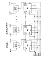
- Fig. 6 schematically depicts a multiplicity of nonvolatile multiconfigurable circuits connected to perform the function of a DIP switch.
- Fig. 7 schematically depicts a multiconfigurable circuit operable in conjunction with analog switches to perform the function of a single pole double throw switch.
- Fig. 8 schematically depicts a multiplicity of nonvolatile multiconfigutable circuits interconnected to perform the functions of a counter.
- a volatile/nonvolatile circuit characterized by a volatile shift register stage having data input, data output and clocking lines, nonvolatile storage means coupled to said volatile shift register stage and responsive to a selective program command to store the binary state stored in the volatile shift register stage, and recall means connected to said volatile shift register stage and to said nonvolatile storage means and responsive to a selective recall command to set said volatile shift register stage to the binary state stored in said nonvolatile storage means, wherein said volatile shift register stage includes first and second sections, said first section including a first inverter having an output connected by a feedback path including a second inverter to the input of said first inverter and said output of said first inverter being coupled via first coupling means to said second section, which includes buffer means coupled to said data output lines, and wherein said nonvolatile storage means includes a floating gate transistor having its floating gate electrode coupled to first and second capacitors which are connected via second coupling means to respective outputs of said second inverter and said first inverter
- the nonvolatile multiconfigurable circuit generally at 1, is comprised of a serial-in serial-out shift register stage 2 connected to a memory device and control 3 by lines 4 and 6.
- Shift register stage 2 is conventional to the extent that data signals are received via data in connection 7 and following a clock cycle are provided as data out signals on data out and data out/lines 8 and 9, respectively.
- shift register stage 2 also includes a clocking connection 11, as well as respective set/ and reset/ connections 12 and 13.
- the transfer of data from nonvolatile memory device and control 3 to shift register stage 2 is responsive to control signals from power-on recall block 19.
- power-on recall 19 is connected to memory device and control 3 by line 22 and to shift register stage 2 by line 23, in such a way that shift register stage 2 can first be preconditioned by a signal on line 23 and thereafter respond to the memory device in block 3 when connected in response to a control signal on line 22.
- a program voltage generator and control block 24 is also depicted in Fig. 1 of the drawings, having as an input a command line 26 and as outputs program line 27 and program voltage (VPP) line 28.
- Program voltage generator and control block 24 provides the signals which program the nonvolatile memory device in block 3.
- program voltage generator and control block 24 receives a write command pulse on line 26 and thereafter generates a timed program signal on line 27 and a relatively large amplitude, specified waveform program voltage VPP on line 28.
- lines 27 and 28 represent that the signals may be generated elsewhere or commonly conveyed by lines 27 and 28 to other adjacent NMCs.
- the common usage of signals is equally applicable to those emanating from power-on recall block 19, in that these signals are, in most cases, common to multiple NMCs, including selective groupings thereof.
- the output of shift register stage 2 controls the on/off state of bidirectional analog switch 16, so as to define an open/close state between in/out line 17 and out/in line 18 of switch 16 which corresponds to the logic state of the signal on data out line 8.
- the on/off state of switch 16 can be defined either by data shifted into register stage 2 or by data transferred into register stage 2 from the nonvolatile memory device and control 3. Note that the high frequency volatile segment of the circuit, block 2, is isolated from the low frequency, endurance limited nonvolatile segment of the circuit, block 3.
- FIG. 2 An illustrative circuit embodying the NMC functions is schematically depicted in Fig. 2 of the drawings.
- the circuit in Fig. 2 illustrates a CMOS embodiment fabricated with a single polysilicon layer.
- the schematic depicts the use of p-channel field effect transistors, such as M1, n-channel field effect transistors, such as M2, a positive voltage supply VDD of approximately +5 volts, ground nodes, a reference voltage node VREF, and programming/ground node shown symbolically by squares, which programming/ground node is normally maintained at ground potential but is pulled to -9 volts during the programming/writing of memory device in block 3 (Fig. 1).
- the top portion of the diagram in Fig. 2 represents the serial-in serial-out shift register stage.
- Field effect transistors M1 and M2 pass the signals connected to the data in line in response to the clock signals (CK and CK/), the CK/ signal being generated by inverter connected transistors M3 and M4.
- the latching of the data into the first section of the shift register is accomplished by transistors M7 and M8 providing in positive feedback form the signal from inverter M5 and M6 following inversion by M10 and M11, the inverters being responsive to reset/ and set/ signals on transistors M24 and M25.
- the second section of the shift register is connected to the first section by clocked pass transistors M12 and M13, which then in succession drive the buffer inverter set comprised of M16, M17, M18 and M19 and the inversely clocked latching feedback path provided by transistors M20 and M21.
- the nonvolatile segment of the NMC is connected to the shift register at nodes 4 and 6.
- the shift register is comprised exclusively of volatile devices, and as such is not subject to the frequency constraints imposed by the extended programming/writing pulses used to program/write the nonvolatile devices.
- the nonvolatile devices is also not exercised in its endurance capacity during shift register operation.
- Field effect transistors M14, M27 and M28 provide the recall function to the NMC, by enabling the access transistor M14 and thereby connecting node 4 with floating gate sense transistor M15.
- node 4 is preconditioned to be at +5 volts in response to an immediately preceding set/ signal to transistor M25. The continuity of the +5 volts on node 4 is thereafter determined, during recall/, by the conductive state of floating gate sense transistor M15.
- Transistors M26 and M32 pass through the bias voltage VREF, nominally +1 volts, to nodes 29 and 31.
- the bias voltage is coupled by capacitors C1 and C2 to floating gate electrode 30, to shift the gate voltage experienced by transistor M15 and thereby optimize its operating window. If the combination of the charge on the floating gate node 30 and the potential of VREF exceeds the threshold of sense field effect transistor M15, transistor M15 conducts in conjunction with M14 to pull node 4 to a low voltage. In the alternative, if the previously written state represented by the charge on node 30 when combined with VREF is inadequate to enable transistor M15, node 4 remains at its high level.
- the nonvolatile information is transferred from the memory device and control section, the floating gate and associated transistors, to the volatile shift register stage. It should be recognized that the use of a single sense transistor in combination with a recall set/cycle during a recall avoids the need for replicating the nonvolatile elements which would otherwise store the inverse of the nonvolatile data.
- Transistor inverter pair M34 and M35 disable transistors M26 and M32 when the nonvolatile section is undergoing programming/writing.
- nodes 4 and 6 are respectively connected to nodes 29 and 31 via transistors M22 and M23.
- nodes 29 and 31 are connected to nodes 4 and 6 during programming/writing, yet are connected to bias voltage VREF during other times of the operating cycle.
- circuit nodes 29 and 31 are held at voltage VREF during the changes of state within the volatile shift register section. Stability in the voltage coupled to the floating gate during dynamic variations in the shift register section maximizes retention in the nonvolatile section of the NMC.
- the transfer of charge onto the nonvolatile floating gate electrode node 30 during programming/writing is accomplished by providing a program signal in substantial time coincidence with the provision of -9 volts VPP to the square designated node.
- These conditions produce a potential difference of 14 volts between nodes 29 and 31, across capacitors C1 and C2, in that the two nodes ate connected to respectively reversed sections of the shift register as represented by the voltages on nodes 4 and 6, wherein one of the nodes is at VDD, +5 volts, while the other node is drawn to the -9 volt VPP via appropriate transistor M6 or M11.
- Capacitor C1 is designed to be approximately 10 times larger than capacitor C2, providing when operated in the manner described above a distributed potential of approximately 14 volts across C2.
- the thin floating gate tunneling dielectric which forms C2 conducts charge in the direction defined by the impressed potential to produce a net positive or negative trapped charge on floating gate node 30.
- an extension of floating gate electrode node 30 is the gate electrode of sensing field effect transistor M15.
- the described invention employs a division of programming/writing voltages which minimize the likelihood of dielectric breakdowns in very large scale integrated circuit devices.
- the selection of programming/writing voltages at +5 volts and -9 volts in conjunction with the conductive paths defined for each voltage ensure that active field effect devices are not subjected to stresses significantly in excess of 14 volts.
- Figure 3 depicts the waveforms of the clock, the data in, and the data out signals, from which waveforms it can be noted that the data in signal must remain valid during the data set up time following the negative transition of the clock. Note that data issuing at the output appears after the positive transition of the clock.
- a representative data set up time is 50 nanoseconds.
- Figure 4 depicts the timing relationship between the recall/, set/, and the data out signals.
- a representative 20 nanoseconds set/ pulse is used to precondition the volatile shift register prior to the recall of nonvolatile data.
- the duration of the recall/signal is nominally 50 nanoseconds, together providing a transfer of nonvolatile data into the shift register in significantly less than 100 nanoseconds.
- the time delay associated with recalling nonvolatile data can be further reduced by using a complementary pair of nonvolatile memory cells or a sense amplifier to drive the voltages on nodes 4 and 6.
- the signals associated with programming/ writing the NMC are depicted in Figure 5.
- the program node is normally held low, and according to preferred embodiment is brought high for approximately 10 milliseconds during the programming/writing operation.
- This waveform can be generated by a program voltage generator and control, such as 24 in Figure 1, or can be provided by outside circuitry.
- the remaining programming signal is the -9 volts of VPP.
- This signal must also be present for approximately 10 milliseconds, and is further constrained by the requirement for a nominal 250 microsecond fall time and a nominal 10 microsecond rise time.
- this signal is common to all NMCs undergoing concurrent programming. This allows a single circuit to control a multiplicity of NMCs.
- Figure 1 illustrates the use of an NMC in combination with bidirectional analog switch 16 to relate the conductive state of switch 16 to the data in shift register stage 2.
- the data state in the shift register can be defined by clocked input data, or by a reset operation, or by a recall of formerly programmed nonvolatile data.
- Figure 6 illustrates the interconnection of multiple NMCs to perform the function of a DIP switch, the corresponding analog switches of which are defined by shifted or recalled data. In a similar way, the switch states could be entered and thereafter stored for future recall.
- the multiple stage embodiment depicted in Figure 6 can also be utilized in trimming resistor ladder networks, coding or decoding of encrypted data, setting of filter break points, controlling oscillator frequencies, and adjusting amplifier gain characteristics, among other applications. Note that nonvolatile programming is the sole low frequency operation.
- NMC NMC-based multi-record data bus
- Figure 7 A further varied application of the NMC is depicted in Figure 7, where the outputs of the NMC are connected to the complementary inputs of two analog switches to create a single pole, double throw switch.
- NMCs Numerous other variations of such switching arrangements are also possible using NMCs, one further example being an integrated circuit equivalent of a rotary switch implemented by commonly connecting one output line from each of multiple analog switches.
- the switch state information can be stored in nonvolatile form for later recall.
- FIG. 8 Further diverse embodiments utilizing an interconnection of multiple NMCs are presented in Figure 8.
- the depicted arrangement illustrates the connection of three NMCs in conjunction with OR gates to create a 3 bit up counter.
- the down counter version of the arrangement can be implemented by taking the output from data out instead of data out/nodes for each NMC.
- the nonvolatile feature provides for the storage and recall of the count.
- the volatile shift register can be selectively set, set by a recall of the stored nonvolatile data, and operated at high frequency without affecting the stored nonvolatile data.
- the data in the shift register can, at any time, be transferred to nonvolatile storage with a single, direct write, programming operation.
- the use of a single polysilicon structure and low programming voltages allow inclusion of the circuit in contemporary integrated circuits, and particularly in semicustom designs configured from cell libraries.
Landscapes
- Read Only Memory (AREA)
- Static Random-Access Memory (AREA)
- Logic Circuits (AREA)
- Semiconductor Integrated Circuits (AREA)
- Shift Register Type Memory (AREA)
Abstract
Description
- This invention relates to a volatile/ nonvolatile circuit, that is, a circuit which is configured to combine the attributes of volatile and nonvolatile functional segments.
- The invention has a particular application to the field of semicustom integrated circuits configured with computer aided design systems using cell library type standardized structures.
- U.S. Patent No. 3,831,155 discloses a nonvolatile semiconductot shift register, which stores in nonvolatile form the data following each shift. This known circuit has the disadvantage that the circuit is subject to relatively rapid retention degradation. Furthetmore, the circuit has a relatively slow operating speed in view of the application of both an erase and a write cycle for each transfer of data through the register.
- Embodiments of the invention will now be described by way of example, with reference to the accompanying drawings, in which:
- Fig. 1 is a functional block diagram of a preferred embodiment of a composite nonvolatile multiconfigurable circuit.
- Fig. 2 is a schematic of a field effect transistor embodiment of the shift register stage and memory device and control functional blocks first depicted in Fig. 1.
- Figs. 3-5 are representative timing diagrams for the schematic in Fig. 2, relating the signals on the clock, data in, data out, set, program, high voltage and recall lines.
- Fig. 6 schematically depicts a multiplicity of nonvolatile multiconfigurable circuits connected to perform the function of a DIP switch.
- Fig. 7 schematically depicts a multiconfigurable circuit operable in conjunction with analog switches to perform the function of a single pole double throw switch.
- Fig. 8 schematically depicts a multiplicity of nonvolatile multiconfigutable circuits interconnected to perform the functions of a counter.
- The document: INTER ELECTRONIQUE, No. 198, 26 January 1976, "Des elements memoires non volatile",
page 21, discloses an integrated circuit including a quadruple latch associated with a four bit MNOS nonvolatile memory. Data transfer from the latch to the MNOS nonvolatile memory and vice versa can be effected by means of input signals on respective input pins of the integrated circuit. - It is an object of the present invention to provide a volatile/nonvolatile circuit which is adapted to operate at a relatively high frequency in volatile operation, which has the ability to store data in nonvolatile form with no erase cycle and minimal endurance degradation, and which is suitable for implementation in a computer aided design cell library.
- Therefore, according to the present invention there is provided a volatile/nonvolatile circuit, characterized by a volatile shift register stage having data input, data output and clocking lines, nonvolatile storage means coupled to said volatile shift register stage and responsive to a selective program command to store the binary state stored in the volatile shift register stage, and recall means connected to said volatile shift register stage and to said nonvolatile storage means and responsive to a selective recall command to set said volatile shift register stage to the binary state stored in said nonvolatile storage means, wherein said volatile shift register stage includes first and second sections, said first section including a first inverter having an output connected by a feedback path including a second inverter to the input of said first inverter and said output of said first inverter being coupled via first coupling means to said second section, which includes buffer means coupled to said data output lines, and wherein said nonvolatile storage means includes a floating gate transistor having its floating gate electrode coupled to first and second capacitors which are connected via second coupling means to respective outputs of said second inverter and said first inverter said first capacitor having a larger capacitance value than said second capacitor whereby, in response to said program command, said second coupling means is enabled, such that said first and second capacitors ate effective to control the charge on said floating gate electrode in accordance with the output signal state of said first inverter.
- The features of the invention can be more fully appreciated by considering a preferred embodiment thereof, as functionally illustrated in Fig. 1 and schematically depicted in Fig. 2 of the drawings. As shown in Fig. 1, the nonvolatile multiconfigurable circuit (NMC), generally at 1, is comprised of a serial-in serial-out
shift register stage 2 connected to a memory device andcontrol 3 bylines Shift register stage 2 is conventional to the extent that data signals are received via data in connection 7 and following a clock cycle are provided as data out signals on data out and data out/lines 8 and 9, respectively. As shown,shift register stage 2 also includes a clocking connection 11, as well as respective set/ and reset/connections - The transfer of data from nonvolatile memory device and
control 3 to shiftregister stage 2 is responsive to control signals from power-onrecall block 19. As is suggested by the title ofblock 19, its purpose is to provide the appropriate sequence of signals which will transfer data from memory device andcontrol 3 to shiftregister stage 2. As presently embodied, power-onrecall 19 is connected to memory device andcontrol 3 byline 22 and to shiftregister stage 2 byline 23, in such a way thatshift register stage 2 can first be preconditioned by a signal online 23 and thereafter respond to the memory device inblock 3 when connected in response to a control signal online 22. - A program voltage generator and
control block 24 is also depicted in Fig. 1 of the drawings, having as an input acommand line 26 and asoutputs program line 27 and program voltage (VPP)line 28. Program voltage generator andcontrol block 24 provides the signals which program the nonvolatile memory device inblock 3. According to the the preferred embodiment, program voltage generator andcontrol block 24 receives a write command pulse online 26 and thereafter generates a timed program signal online 27 and a relatively large amplitude, specified waveform program voltage VPP online 28. - The dashed leftward projections, of
lines lines recall block 19, in that these signals are, in most cases, common to multiple NMCs, including selective groupings thereof. - In an exemplary use of the NMC, the output of
shift register stage 2, for example online 14, controls the on/off state of bidirectionalanalog switch 16, so as to define an open/close state between in/outline 17 and out/inline 18 ofswitch 16 which corresponds to the logic state of the signal on data out line 8. With this configuration, the on/off state ofswitch 16 can be defined either by data shifted intoregister stage 2 or by data transferred intoregister stage 2 from the nonvolatile memory device andcontrol 3. Note that the high frequency volatile segment of the circuit,block 2, is isolated from the low frequency, endurance limited nonvolatile segment of the circuit,block 3. - An illustrative circuit embodying the NMC functions is schematically depicted in Fig. 2 of the drawings. The circuit in Fig. 2 illustrates a CMOS embodiment fabricated with a single polysilicon layer. The schematic depicts the use of p-channel field effect transistors, such as M1, n-channel field effect transistors, such as M2, a positive voltage supply VDD of approximately +5 volts, ground nodes, a reference voltage node VREF, and programming/ground node shown symbolically by squares, which programming/ground node is normally maintained at ground potential but is pulled to -9 volts during the programming/writing of memory device in block 3 (Fig. 1).
- The top portion of the diagram in Fig. 2 represents the serial-in serial-out shift register stage. Field effect transistors M1 and M2 pass the signals connected to the data in line in response to the clock signals (CK and CK/), the CK/ signal being generated by inverter connected transistors M3 and M4. The latching of the data into the first section of the shift register is accomplished by transistors M7 and M8 providing in positive feedback form the signal from inverter M5 and M6 following inversion by M10 and M11, the inverters being responsive to reset/ and set/ signals on transistors M24 and M25. The second section of the shift register is connected to the first section by clocked pass transistors M12 and M13, which then in succession drive the buffer inverter set comprised of M16, M17, M18 and M19 and the inversely clocked latching feedback path provided by transistors M20 and M21. The nonvolatile segment of the NMC is connected to the shift register at
nodes - Note that the shift register is comprised exclusively of volatile devices, and as such is not subject to the frequency constraints imposed by the extended programming/writing pulses used to program/write the nonvolatile devices. As a corollary, the nonvolatile devices is also not exercised in its endurance capacity during shift register operation.
- Field effect transistors M14, M27 and M28 provide the recall function to the NMC, by enabling the access transistor M14 and thereby connecting
node 4 with floating gate sense transistor M15. At the time the recall/ function is initiated,node 4 is preconditioned to be at +5 volts in response to an immediately preceding set/ signal to transistor M25. The continuity of the +5 volts onnode 4 is thereafter determined, during recall/, by the conductive state of floating gate sense transistor M15. - Transistors M26 and M32 pass through the bias voltage VREF, nominally +1 volts, to
nodes gate electrode 30, to shift the gate voltage experienced by transistor M15 and thereby optimize its operating window. If the combination of the charge on thefloating gate node 30 and the potential of VREF exceeds the threshold of sense field effect transistor M15, transistor M15 conducts in conjunction with M14 to pullnode 4 to a low voltage. In the alternative, if the previously written state represented by the charge onnode 30 when combined with VREF is inadequate to enable transistor M15,node 4 remains at its high level. Thereby, the nonvolatile information is transferred from the memory device and control section, the floating gate and associated transistors, to the volatile shift register stage. It should be recognized that the use of a single sense transistor in combination with a recall set/cycle during a recall avoids the need for replicating the nonvolatile elements which would otherwise store the inverse of the nonvolatile data. - Transistor inverter pair M34 and M35 disable transistors M26 and M32 when the nonvolatile section is undergoing programming/writing. During
such programming nodes nodes nodes nodes - It is worth noting that among other features of the
circuit nodes - The transfer of charge onto the nonvolatile floating
gate electrode node 30 during programming/writing is accomplished by providing a program signal in substantial time coincidence with the provision of -9 volts VPP to the square designated node. These conditions produce a potential difference of 14 volts betweennodes nodes gate node 30. Note that an extension of floatinggate electrode node 30 is the gate electrode of sensing field effect transistor M15. - It should be appreciated that the described invention employs a division of programming/writing voltages which minimize the likelihood of dielectric breakdowns in very large scale integrated circuit devices. The selection of programming/writing voltages at +5 volts and -9 volts in conjunction with the conductive paths defined for each voltage ensure that active field effect devices are not subjected to stresses significantly in excess of 14 volts.
- Representative signal timing relationships suitable to operate
NMC 1 depict in Figure 2 appear in Figures 3-5. Figure 3 depicts the waveforms of the clock, the data in, and the data out signals, from which waveforms it can be noted that the data in signal must remain valid during the data set up time following the negative transition of the clock. Note that data issuing at the output appears after the positive transition of the clock. A representative data set up time is 50 nanoseconds. - Figure 4 depicts the timing relationship between the recall/, set/, and the data out signals. A representative 20 nanoseconds set/ pulse is used to precondition the volatile shift register prior to the recall of nonvolatile data. The duration of the recall/signal is nominally 50 nanoseconds, together providing a transfer of nonvolatile data into the shift register in significantly less than 100 nanoseconds. The time delay associated with recalling nonvolatile data can be further reduced by using a complementary pair of nonvolatile memory cells or a sense amplifier to drive the voltages on
nodes - The signals associated with programming/ writing the NMC are depicted in Figure 5. Note that the program node is normally held low, and according to preferred embodiment is brought high for approximately 10 milliseconds during the programming/writing operation. This waveform can be generated by a program voltage generator and control, such as 24 in Figure 1, or can be provided by outside circuitry. The remaining programming signal is the -9 volts of VPP. This signal must also be present for approximately 10 milliseconds, and is further constrained by the requirement for a nominal 250 microsecond fall time and a nominal 10 microsecond rise time. The feature worth noting is that this signal is common to all NMCs undergoing concurrent programming. This allows a single circuit to control a multiplicity of NMCs.
- The combination of volatile and nonvolatile capabilities in a single circuit provides the user with significant versatility as to the electronic functions which can be implemented. Figure 1 illustrates the use of an NMC in combination with
bidirectional analog switch 16 to relate the conductive state ofswitch 16 to the data inshift register stage 2. The data state in the shift register can be defined by clocked input data, or by a reset operation, or by a recall of formerly programmed nonvolatile data. The fundamental concepts can be extended in numerous ways. For example, Figure 6 illustrates the interconnection of multiple NMCs to perform the function of a DIP switch, the corresponding analog switches of which are defined by shifted or recalled data. In a similar way, the switch states could be entered and thereafter stored for future recall. The multiple stage embodiment depicted in Figure 6 can also be utilized in trimming resistor ladder networks, coding or decoding of encrypted data, setting of filter break points, controlling oscillator frequencies, and adjusting amplifier gain characteristics, among other applications. Note that nonvolatile programming is the sole low frequency operation. - A further varied application of the NMC is depicted in Figure 7, where the outputs of the NMC are connected to the complementary inputs of two analog switches to create a single pole, double throw switch. Numerous other variations of such switching arrangements are also possible using NMCs, one further example being an integrated circuit equivalent of a rotary switch implemented by commonly connecting one output line from each of multiple analog switches. Again, the switch state information can be stored in nonvolatile form for later recall.
- Further diverse embodiments utilizing an interconnection of multiple NMCs are presented in Figure 8. The depicted arrangement illustrates the connection of three NMCs in conjunction with OR gates to create a 3 bit up counter. The down counter version of the arrangement can be implemented by taking the output from data out instead of data out/nodes for each NMC. Again, the nonvolatile feature provides for the storage and recall of the count.
- With a understanding of the central features which characterize the present NMC invention, one can now more fully appreciate the attributes noted individually hereinbefore. For instance, the volatile shift register can be selectively set, set by a recall of the stored nonvolatile data, and operated at high frequency without affecting the stored nonvolatile data. The data in the shift register can, at any time, be transferred to nonvolatile storage with a single, direct write, programming operation. The use of a single polysilicon structure and low programming voltages allow inclusion of the circuit in contemporary integrated circuits, and particularly in semicustom designs configured from cell libraries.
Claims (8)
Applications Claiming Priority (2)
| Application Number | Priority Date | Filing Date | Title |
|---|---|---|---|
| US06/889,543 US4754432A (en) | 1986-07-25 | 1986-07-25 | Nonvolatile multiconfigurable circuit |
| US889543 | 1986-07-25 |
Publications (2)
| Publication Number | Publication Date |
|---|---|
| EP0275286A1 EP0275286A1 (en) | 1988-07-27 |
| EP0275286B1 true EP0275286B1 (en) | 1991-11-21 |
Family
ID=25395326
Family Applications (1)
| Application Number | Title | Priority Date | Filing Date |
|---|---|---|---|
| EP87904792A Expired - Lifetime EP0275286B1 (en) | 1986-07-25 | 1987-07-20 | Volatile/nonvolatile integrated circuit |
Country Status (5)
| Country | Link |
|---|---|
| US (1) | US4754432A (en) |
| EP (1) | EP0275286B1 (en) |
| JP (1) | JPH01500381A (en) |
| DE (1) | DE3774683D1 (en) |
| WO (1) | WO1988001095A2 (en) |
Families Citing this family (6)
| Publication number | Priority date | Publication date | Assignee | Title |
|---|---|---|---|---|
| US4744062A (en) * | 1985-04-23 | 1988-05-10 | Hitachi, Ltd. | Semiconductor integrated circuit with nonvolatile memory |
| US5452250A (en) * | 1994-06-14 | 1995-09-19 | International Business Machines, Inc. | Non-volatile register system utilizing thin-film floating-gate amorphous transistors |
| US5557272A (en) * | 1994-06-16 | 1996-09-17 | International Business Machines Corporation | Non-volatile serial-to-parallel converter system utilizing thin-film, floating-gate, amorphous transistors |
| US5543791A (en) * | 1994-06-16 | 1996-08-06 | International Business Machines | Non-volatile parallel-to-serial converter system utilizing thin-film floating-gate, amorphous transistors |
| US5912937A (en) * | 1997-03-14 | 1999-06-15 | Xilinx, Inc. | CMOS flip-flop having non-volatile storage |
| KR102112367B1 (en) * | 2013-02-12 | 2020-05-18 | 가부시키가이샤 한도오따이 에네루기 켄큐쇼 | Semiconductor device |
Family Cites Families (5)
| Publication number | Priority date | Publication date | Assignee | Title |
|---|---|---|---|---|
| US3831155A (en) * | 1971-12-29 | 1974-08-20 | Tokyo Shibaura Electric Co | Nonvolatile semiconductor shift register |
| US4138737A (en) * | 1978-03-08 | 1979-02-06 | Westinghouse Electric Corp. | Non-volatile memory with improved readout |
| FR2525416A1 (en) * | 1982-04-20 | 1983-10-21 | Efcis | COUNTER WITH NON-VOLATILE BACKUP OF ITS CONTENT |
| US4683554A (en) * | 1985-09-13 | 1987-07-28 | Ncr Corporation | Direct write nonvolatile memory cells |
| US4686652A (en) * | 1985-11-25 | 1987-08-11 | Rockwell International Corporation | Non-volatile RAM cell with single high voltage precharge |
-
1986
- 1986-07-25 US US06/889,543 patent/US4754432A/en not_active Expired - Lifetime
-
1987
- 1987-07-20 EP EP87904792A patent/EP0275286B1/en not_active Expired - Lifetime
- 1987-07-20 WO PCT/US1987/001673 patent/WO1988001095A2/en not_active Ceased
- 1987-07-20 JP JP62504168A patent/JPH01500381A/en active Pending
- 1987-07-20 DE DE8787904792T patent/DE3774683D1/en not_active Expired - Lifetime
Non-Patent Citations (1)
| Title |
|---|
| Inter Electronique, no. 198, 26 January 1976 (Paris, FR) "Des éléments mémoires non volatiles", page 21, voir le document en entier * |
Also Published As
| Publication number | Publication date |
|---|---|
| WO1988001095A2 (en) | 1988-02-11 |
| US4754432A (en) | 1988-06-28 |
| EP0275286A1 (en) | 1988-07-27 |
| JPH01500381A (en) | 1989-02-09 |
| DE3774683D1 (en) | 1992-01-02 |
| WO1988001095A3 (en) | 1988-07-28 |
Similar Documents
| Publication | Publication Date | Title |
|---|---|---|
| US5412601A (en) | Non-volatile semiconductor memory device capable of storing multi-value data in each memory cell | |
| US5859544A (en) | Dynamic configurable elements for programmable logic devices | |
| US5450341A (en) | Non-volatile semiconductor memory device having memory cells, each for at least three different data writable thereinto selectively and a method of using the same | |
| US5047985A (en) | Static random access memory device having a high speed read-out and precharging arrangement | |
| JPS5930302B2 (en) | Program information | |
| JPH0369095A (en) | Storage cells used in storage logic arrays with two-conductor data columns | |
| GB2084828A (en) | Semiconductor ic memory | |
| JPH03231515A (en) | Programmable logic device | |
| US4000429A (en) | Semiconductor circuit device | |
| EP0030130A1 (en) | An oscillator and an EPROM including such an oscillator | |
| US4754432A (en) | Nonvolatile multiconfigurable circuit | |
| JPH021456B2 (en) | ||
| JP2000011674A (en) | Latch type sense circuit and program verify circuit | |
| JPS6053000A (en) | Integrated memory circuit | |
| US6208564B1 (en) | High voltage comparator | |
| US4333166A (en) | Semiconductor memory circuits | |
| US6266279B1 (en) | Nonvolatile semiconductor memory device, method for reading data from the nonvolatile semiconductor memory device, and method for writing data into the nonvolatile semiconductor memory device | |
| TW201820333A (en) | Boost circuit and non-volatile memory having the same | |
| JPH0115958B2 (en) | ||
| US4860258A (en) | Electrically programmable non-volatile memory having sequentially deactivated write circuits | |
| US4856034A (en) | Semiconductor integrated circuit | |
| KR100591571B1 (en) | High speed address sequencer | |
| KR950004863B1 (en) | Eprom latch circuit | |
| JP2001043688A (en) | Flash memory circuit | |
| JP2000014130A (en) | Booster |
Legal Events
| Date | Code | Title | Description |
|---|---|---|---|
| PUAI | Public reference made under article 153(3) epc to a published international application that has entered the european phase |
Free format text: ORIGINAL CODE: 0009012 |
|
| AK | Designated contracting states |
Kind code of ref document: A1 Designated state(s): DE GB NL |
|
| D17D | Deferred search report published (deleted) | ||
| 17P | Request for examination filed |
Effective date: 19890114 |
|
| 17Q | First examination report despatched |
Effective date: 19900810 |
|
| GRAA | (expected) grant |
Free format text: ORIGINAL CODE: 0009210 |
|
| AK | Designated contracting states |
Kind code of ref document: B1 Designated state(s): DE GB NL |
|
| REF | Corresponds to: |
Ref document number: 3774683 Country of ref document: DE Date of ref document: 19920102 |
|
| PLBE | No opposition filed within time limit |
Free format text: ORIGINAL CODE: 0009261 |
|
| STAA | Information on the status of an ep patent application or granted ep patent |
Free format text: STATUS: NO OPPOSITION FILED WITHIN TIME LIMIT |
|
| 26N | No opposition filed | ||
| REG | Reference to a national code |
Ref country code: GB Ref legal event code: 732E |
|
| NLS | Nl: assignments of ep-patents |
Owner name: NCR INTERNATIONAL INC. TE DAYTON, OHIO, VER. ST. V |
|
| NLT1 | Nl: modifications of names registered in virtue of documents presented to the patent office pursuant to art. 16 a, paragraph 1 |
Owner name: AT&T GLOBAL INFORMATION SOLUTIONS INTERNATIONAL IN |
|
| REG | Reference to a national code |
Ref country code: GB Ref legal event code: 732E |
|
| REG | Reference to a national code |
Ref country code: GB Ref legal event code: 732E |
|
| NLS | Nl: assignments of ep-patents |
Owner name: AT&T GLOBAL INFORMATION SOLUTIONS INTERNATIONAL IN |
|
| NLS | Nl: assignments of ep-patents |
Owner name: AT&T GLOBAL INFORMATION SOLUTIONS INTERNATIONAL IN |
|
| NLT1 | Nl: modifications of names registered in virtue of documents presented to the patent office pursuant to art. 16 a, paragraph 1 |
Owner name: NCR INTERNATIONAL, INC;HYUNDAI ELECTRONICS AMERICA |
|
| NLT1 | Nl: modifications of names registered in virtue of documents presented to the patent office pursuant to art. 16 a, paragraph 1 |
Owner name: NCR INTERNATIONAL, INC;HYUNDAI ELECTRONICS AMERICA |
|
| REG | Reference to a national code |
Ref country code: GB Ref legal event code: IF02 |
|
| NLS | Nl: assignments of ep-patents |
Owner name: NCR INTERNATIONAL, INC Owner name: HYNIX SEMICONDUCTOR INC. Owner name: HYUNDAI ELECTRONICS AMERICA |
|
| NLT1 | Nl: modifications of names registered in virtue of documents presented to the patent office pursuant to art. 16 a, paragraph 1 |
Owner name: HYNIX SEMICONDUCTOR AMERICA INC. Owner name: NCR INTERNATIONAL, INC |
|
| REG | Reference to a national code |
Ref country code: GB Ref legal event code: 732E |
|
| PGFP | Annual fee paid to national office [announced via postgrant information from national office to epo] |
Ref country code: NL Payment date: 20050703 Year of fee payment: 19 |
|
| PGFP | Annual fee paid to national office [announced via postgrant information from national office to epo] |
Ref country code: DE Payment date: 20050714 Year of fee payment: 19 |
|
| PGFP | Annual fee paid to national office [announced via postgrant information from national office to epo] |
Ref country code: GB Payment date: 20050720 Year of fee payment: 19 |
|
| PG25 | Lapsed in a contracting state [announced via postgrant information from national office to epo] |
Ref country code: GB Free format text: LAPSE BECAUSE OF NON-PAYMENT OF DUE FEES Effective date: 20060720 |
|
| NLS | Nl: assignments of ep-patents |
Owner name: NCR INTERNATIONAL, INC Effective date: 20060913 Owner name: MAGNACHIP SEMICONDUCTOR LTD. Effective date: 20060913 |
|
| PG25 | Lapsed in a contracting state [announced via postgrant information from national office to epo] |
Ref country code: NL Free format text: LAPSE BECAUSE OF NON-PAYMENT OF DUE FEES Effective date: 20070201 Ref country code: DE Free format text: LAPSE BECAUSE OF NON-PAYMENT OF DUE FEES Effective date: 20070201 |
|
| GBPC | Gb: european patent ceased through non-payment of renewal fee |
Effective date: 20060720 |
|
| NLV4 | Nl: lapsed or anulled due to non-payment of the annual fee |
Effective date: 20070201 |