EP0272476B1 - High density vmos dynamic ram array - Google Patents
High density vmos dynamic ram array Download PDFInfo
- Publication number
- EP0272476B1 EP0272476B1 EP87117303A EP87117303A EP0272476B1 EP 0272476 B1 EP0272476 B1 EP 0272476B1 EP 87117303 A EP87117303 A EP 87117303A EP 87117303 A EP87117303 A EP 87117303A EP 0272476 B1 EP0272476 B1 EP 0272476B1
- Authority
- EP
- European Patent Office
- Prior art keywords
- trenches
- layer
- doped
- polysilicon
- substrate
- Prior art date
- Legal status (The legal status is an assumption and is not a legal conclusion. Google has not performed a legal analysis and makes no representation as to the accuracy of the status listed.)
- Expired - Lifetime
Links
Images

Classifications
-
- H—ELECTRICITY
- H01—ELECTRIC ELEMENTS
- H01L—SEMICONDUCTOR DEVICES NOT COVERED BY CLASS H10
- H01L21/00—Processes or apparatus adapted for the manufacture or treatment of semiconductor or solid state devices or of parts thereof
- H01L21/70—Manufacture or treatment of devices consisting of a plurality of solid state components formed in or on a common substrate or of parts thereof; Manufacture of integrated circuit devices or of parts thereof
- H01L21/71—Manufacture of specific parts of devices defined in group H01L21/70
- H01L21/74—Making of localized buried regions, e.g. buried collector layers, internal connections substrate contacts
- H01L21/743—Making of internal connections, substrate contacts
-
- H—ELECTRICITY
- H01—ELECTRIC ELEMENTS
- H01L—SEMICONDUCTOR DEVICES NOT COVERED BY CLASS H10
- H01L21/00—Processes or apparatus adapted for the manufacture or treatment of semiconductor or solid state devices or of parts thereof
- H01L21/70—Manufacture or treatment of devices consisting of a plurality of solid state components formed in or on a common substrate or of parts thereof; Manufacture of integrated circuit devices or of parts thereof
- H01L21/77—Manufacture or treatment of devices consisting of a plurality of solid state components or integrated circuits formed in, or on, a common substrate
- H01L21/78—Manufacture or treatment of devices consisting of a plurality of solid state components or integrated circuits formed in, or on, a common substrate with subsequent division of the substrate into plural individual devices
- H01L21/82—Manufacture or treatment of devices consisting of a plurality of solid state components or integrated circuits formed in, or on, a common substrate with subsequent division of the substrate into plural individual devices to produce devices, e.g. integrated circuits, each consisting of a plurality of components
- H01L21/822—Manufacture or treatment of devices consisting of a plurality of solid state components or integrated circuits formed in, or on, a common substrate with subsequent division of the substrate into plural individual devices to produce devices, e.g. integrated circuits, each consisting of a plurality of components the substrate being a semiconductor, using silicon technology
- H01L21/8221—Three dimensional integrated circuits stacked in different levels
-
- H—ELECTRICITY
- H10—SEMICONDUCTOR DEVICES; ELECTRIC SOLID-STATE DEVICES NOT OTHERWISE PROVIDED FOR
- H10B—ELECTRONIC MEMORY DEVICES
- H10B12/00—Dynamic random access memory [DRAM] devices
- H10B12/30—DRAM devices comprising one-transistor - one-capacitor [1T-1C] memory cells
- H10B12/39—DRAM devices comprising one-transistor - one-capacitor [1T-1C] memory cells the capacitor and the transistor being in a same trench
- H10B12/395—DRAM devices comprising one-transistor - one-capacitor [1T-1C] memory cells the capacitor and the transistor being in a same trench the transistor being vertical
Definitions
- the present invention relates to dynamic random access semiconductor memory storage cells and, more particularly, to vertically configured MOS memory cell devices including trench capacitors.
- a semiconductor memory which has at least one VMOS transistor which includes a trench and a storage capacitor.
- a semiconductor substrate is doped with concentration centers of a first conductivity type and has a buried layer which is doped with concentration centers of a second conductivity type opposite to the first conductivity type.
- At least two additional layers are divided by the trench and have alternately differing conductivity types, the two additional layers and the buried layer being produced by diffusion and/or implantation.
- U.S. Patent 4,225,879, issued September 30, 1980 to Vinson entitled V-MOS FIELD EFFECT TRANSISTOR FOR A DYNAMIC MEMORY CELL HAVING IMPROVED CAPACITANCE relates to a V-MOS field effect transistor which is provided with enhanced source capacitance to provide a single transistor dynamic memory cell.
- the formation of the source area is achieved by masking the silicon substrate, opening an aperture in the mask and then etching the silicon substrate in such a manner as to undercut the mask so that the mask provides a shield to subsequent ion implanting of the source area.
- Both P and N type dopants are separately implanted with different energy levels so as to form an enhanced PN junction capacitance for the device.
- U.S. Patent 4,326,332, issued April 27, 1982 to Kenney entitled METHOD OF MAKING A HIGH DENSITY V-MOS MEMORY ARRAY describes a method for providing high density dynamic memory cells which provides self-alignment of both V-MOSFET device elements and their interconnections through the use of a device-defining masking layer having a plurality of parallel thick and thin regions. Holes are etched in portions of the thin regions with the use of an etch mask defining a plurality of parallel regions aligned perpendicular to the regions in the masking layer. V-MOSFET devices having self-aligned gate electrodes are formed in the holes and device interconnecting lines are formed under the remaining portions of the thin regions. A combination of anisotropic etching and directionally dependent etching, such as reactive ion etching, is used to extend the depth of V-grooves.
- a semiconductor memory device comprised of an integrated array of cells formed on a substrate in conjunction with parallel spaced-apart bit lines and conductive word lines that are perpendicular to the bit lines.
- a plurality of V-shaped recesses are located between and extend perpendicular to adjacent parallel bit lines.
- Two cells share each recess and each cell includes a VMOS transistor formed by one end portion of the recess and an isolated buried source region located under the adjacent bit line.
- a channel stop region is located between and isolates the VMOS transistors and their respective buried source regions at opposite ends of each recess.
- a method of manufacturing a MOS semiconductor device which comprises a step of forming a groove in a predetermined portion of a semiconductor substrate, a step of forming a gate insulation film to cover the entire surface of the substrate inclusive of the groove, a step of depositing a gate electrode material to a thickness greater than one half the width of the opening of the groove to thereby fill the groove with the gate electrode material, and a step of forming a gate electrode within the groove by etching away the gate electrode material until the gate insulation film other than that within the groove is exposed.
- U.S. Patent 4,353,086, issued October 5, 1982 to Jaccodine et al entitled SILICON INTEGRATED CIRCUITS describes a dynamic random access memory in which individual cells, including an access transistor and a storage capacitor, are formed in mesas formed on a silicon chip.
- the access transistor of the cell is formed on the top surface of the mesa and one plate of the storage capacitor of the cell is formed by the sidewall of the mesa and the other plate by doped polycrystalline silicon which fills the grooves surrounding the mesas isolated therefrom by a silicon dioxide layer.
- the mesas may include other forms of circuit elements.
- Japanese Patent 55-11365(A), issued January 26, 1980 entitled SEMICONDUCTOR MEMORY describes a technique for increasing a capacity section in a capacitor without increasing the size of cell surface, by providing in a semiconductor substrate a recess contacting with a source and drain range and a source range through the medium of insulating film.
- the invention as claimed solves the problem of providing a vertical DRAM cell using VMOS transistors and trench capacitors and the fabrication process therefor wherein the array needs only a single level of polysilicon and has no contacts.
- the present invention provides a vertical DRAM structure comprising a VMOS transistor and trench capacitor in combination wherein the access transistors are in a V-groove and one electrode of the capacitor is in the trench and the other electrode is the substrate.
- a vertical DRAM cell using VMOS transistors and trench capacitors is shown requiring only a single level of polysilicon and no contacts.
- the memory cell circuit is that of the conventional one-device memory cell, having a single access transistor with its gate connected to a word line, its drain connected to a bit line, and its source connected to a storage capacitor.
- an array with n-type devices is shown.
- the storage capacitance node 16 is connected to the source 22 of the V-groove access device through a conducting bridge 18.
- the gate of the V-groove access device is connected to polysilicon word line 40 and the drain is diffused region 30 which also serves as the bit line of the cell.
- the substrate region 26 of the V-groove device is an epitaxially grown layer.
- the single crystal epitaxial layer 26 is grown over a combination of single crystalline material and oxide. Polycrystalline regions in the silicon substrate 10 have an oxide covering. In an alternate version, it is assumed that it is possible to grow a single crystal epitaxial layer over regions consisting of both single crystal and poly crystal Si or that it is possible to convert polycrystalline material on top of single crystalline material into single crystalline material.
- the structure uses the two sides of a V-groove to form the access device for two separate cells.
- the V-groove divides the upper n+ region 30 into two drain regions, one for each access device and also divides the lower n+ region 22 into two source regions which are connected to their respective capacitor nodes 16.
- the channels for the two access devices are along the sides of the V-groove. This results in high density memory cells since the bit line is stacked above the trench storage capacitor and the cell transistor is vertically oriented.
- the cell has a diffused bit line and polysilicon or polycide word line. Contacts and metal would only be needed if the word line had to be stitched.
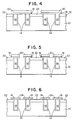
- Step 1 a semiconductor substrate 10, for example p+ silicon, is masked and etched by conventional techniques to form trenches 12 as shown in FIG. 2.
- storage capacitor oxide insulation layer 14 is grown on the surfaces of the substrate and the trenches.
- the trenches are filled with n+ polysilicon 16 and the structure is planarized to remove the oxide 14 and excess polysilicon from the surface of substrate 10 by conventional techniques.
- the removed material is shown in dashed lines in FIG 3.
- Oxide layer 20 is grown or deposited over the polysilicon layer 18 and, using a second mask and conventional etching technique, the polysilicon 18 and oxide 20 is patterned as shown in FIG. 4.
- An n+ diffusion 22 is formed in substrate 10 between non-adjacent trenches, also as shown in FIG. 4. The overlap between regions 18 and 22 results in a conductive connection between them.
- a layer of oxide is grown or conformally deposited over the top of the structure, and anisotropically reactive ion etched in the vertical direction only, as is well known in the art, so that oxide 24 covers the polysilicon and the single crystal silicon substrate 10 surface is exposed as shown in FIG. 6.
- the step of etching the oxide in FIG. 6 is one of the key process steps.
- the etching is directional, such as accomplished by RIE, to remove material in the vertical direction only.
- the purpose of this step is to remove the oxide over the single crystal silicon while keeping a layer 24 of SiO2 on the polycrystalline silicon 18.
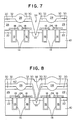
- FIG. 7 illustrates the results of a number of subsequent steps including growing the layer 26 of single crystal epi as described above, defining and growing recessed oxide regions 28 by conventional processes using a fourth mask, forming n+ regions 30, a further layer 32 produced by oxidation, and opening a V-groove 34 using a fifth mask and conventional V-groove etching.
- the V-groove 34 in FIG. 7 is used to form two access devices oriented along the surfaces of the V-groove and to divide the n+ region 22 connecting the non-adjacent trenches and the upper n+ layer 30 such that two separate storage capacitors (the regions 22 and 16 on each side of the V-groove 34) and two separate bit lines (the regions 30 on each side of the V-groove 34) are created.
- the results of the step of growing an oxide layer 38 for the gate oxide is illustrated as well as the deposition and patterning of polysilicon layer 40 which forms the device word line.
- the polysilicon can optionally have a polycide layer for improved conduction. Contacts and metal would only be needed for the cell array if the word line had to be stitched, and they would be formed using conventional techniques.
- a p+ implant can be used to provide isolation between the cells along the V-groove or oxide or trench isolation can be provided.
- bit line is stacked above the trench storage capacitor and the cell transistor is vertically oriented.
- the cell has a diffused bit line and polysilicon or polycide word line.
- the overlay tolerance of the polysilicon "bridge" 18 to the n+ polysilicon 16 which is used to fill the trench directly impacts the density of the cell.
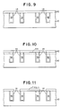
- a layer of polycrystalline silicon 42 such as shown in FIG. 9, is provided after the steps of FIG. 3.
- the layer 42 is converted to single crystalline material by a process such as rapid thermal annealing.
- a mask then can be used to form the n+ doped region (region 22 in FIG. 4).
- the extent of the implant area as a result of the implant is shown by the dashed lines in FIG. 10.
- a vertical DRAM cell and a fabrication process therefor using VMOS transistors and a trench storage capacitor has been described and illustrated.
- This relatively simple cell structure offers the potential for extremely high density.
- the array has only a single level of polysilicon and has no contacts.
- n+ poly used to fill the trench is covered by a layer of SiO2 was described.
- the exposed single crystal regions allow seeding of single crystal epi growth over the SiO2 areas from the exposed single crystal areas of the substrate.
- Other embodiments of the device were also described which require that polycrystalline silicon be converted to single crystalline material by some process such as rapid thermal annealing or that an epitaxial layer of single crystalline silicon be grown over regions of both polycrystalline and single crystalline silicon.
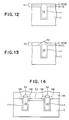
- FIG. 12 A simplified process sequence needed to achieve this structure is shown in FIG. 12.
- the trench is etched using a nitride/oxide first masking layer 50.
- the storage oxide 14 is grown and the trench is filled with the n+ polysilicon 16.
- SiO2 52 is grown over the trench polysilicon 16 and, as shown in FIG. 14, the nitride/oxide layer 50 is then removed, an n+ arsenic diffusion region 54 is created by conventional patterning and masking and a p- epitaxial layer 56 is grown over the entire wafer as shown in FIG. 14.
- Out diffusion 58 from the n+ polysilicon 16 and the n+ region 54 forms a conducting bridge between polysilicon region 16 and diffused region 54.
Description
- The present invention relates to dynamic random access semiconductor memory storage cells and, more particularly, to vertically configured MOS memory cell devices including trench capacitors.
- Various configurations of VMOS devices and trench capacitors are known in the prior art.
- In U.S. Patent 4,156,289, issued May 22, 1979 to Hoffmann et al, entitled SEMICONDUCTOR MEMORY, a semiconductor memory is disclosed which has at least one VMOS transistor which includes a trench and a storage capacitor. A semiconductor substrate is doped with concentration centers of a first conductivity type and has a buried layer which is doped with concentration centers of a second conductivity type opposite to the first conductivity type. At least two additional layers are divided by the trench and have alternately differing conductivity types, the two additional layers and the buried layer being produced by diffusion and/or implantation.
- U.S. Patent 4,225,879, issued September 30, 1980 to Vinson entitled V-MOS FIELD EFFECT TRANSISTOR FOR A DYNAMIC MEMORY CELL HAVING IMPROVED CAPACITANCE, relates to a V-MOS field effect transistor which is provided with enhanced source capacitance to provide a single transistor dynamic memory cell. The formation of the source area is achieved by masking the silicon substrate, opening an aperture in the mask and then etching the silicon substrate in such a manner as to undercut the mask so that the mask provides a shield to subsequent ion implanting of the source area. Both P and N type dopants are separately implanted with different energy levels so as to form an enhanced PN junction capacitance for the device.
- U.S. Patent 4,222,063, issued September 9, 1980 to Rodgers entitled VMOS FLOATING GATE MEMORY WITH BREAKDOWN VOLTAGE LOWERING REGION, describes a semiconductor electrically programmable read only memory device which utilizes an array of memory cells each in the form of a single V-type MOSFET which achieves the normal AND function (Data-Word Address) using a capacitance coupled version of threshold logic. Each MOSFET is formed by a V-shaped recess at the intersection of each bit line and word line that extends across the diffused bit line, (which serves as the transistor drain) and into the substrate (which serves as the source and ground plane of the device).
- U.S. Patent 4,364,074, issued Dec. 14, 1982 to Garnache et al entitled V-MOS DEVICE WITH SELF-ALIGNED MULTIPLE ELECTRODES, teaches that high density VMOSFET devices, particularly single transistor memory cells, are provided by use of a series of simplified self-aligning process steps. Gate electrodes, source/drain regions and source/drain contacts are provided with the aid of an initial mask-less photoresist removal process in which a relatively thick layer of self-leveling photoresist is uniformly removed in order to define portions of a gate electrode within the recess of a V-groove. The gate electrode subsequently acts as a self-aligned mask to define implanted source/drain regions also within the V-groove and to enable second level interconnecting metallurgy contacts to be formed along the sidewalls of the V-groove.
- U.S. Patent 4,326,332, issued April 27, 1982 to Kenney entitled METHOD OF MAKING A HIGH DENSITY V-MOS MEMORY ARRAY, describes a method for providing high density dynamic memory cells which provides self-alignment of both V-MOSFET device elements and their interconnections through the use of a device-defining masking layer having a plurality of parallel thick and thin regions. Holes are etched in portions of the thin regions with the use of an etch mask defining a plurality of parallel regions aligned perpendicular to the regions in the masking layer. V-MOSFET devices having self-aligned gate electrodes are formed in the holes and device interconnecting lines are formed under the remaining portions of the thin regions. A combination of anisotropic etching and directionally dependent etching, such as reactive ion etching, is used to extend the depth of V-grooves.
- In U.S. Patent 4,369,564, issued January 25, 1983 to Hiltpold entitled VMOS MEMORY CELL AND METHOD FOR MAKING SAME, a semiconductor memory device is provided comprised of an integrated array of cells formed on a substrate in conjunction with parallel spaced-apart bit lines and conductive word lines that are perpendicular to the bit lines. A plurality of V-shaped recesses are located between and extend perpendicular to adjacent parallel bit lines. Two cells share each recess and each cell includes a VMOS transistor formed by one end portion of the recess and an isolated buried source region located under the adjacent bit line. A channel stop region is located between and isolates the VMOS transistors and their respective buried source regions at opposite ends of each recess.
- In U.S. Patent 4,455,740, issued June 26, 1984 to Iwai entitled METHOD OF MANUFACTURING A SELF-ALIGNED U-MOS SEMICONDUCTOR DEVICE, a method of manufacturing a MOS semiconductor device is disclosed which comprises a step of forming a groove in a predetermined portion of a semiconductor substrate, a step of forming a gate insulation film to cover the entire surface of the substrate inclusive of the groove, a step of depositing a gate electrode material to a thickness greater than one half the width of the opening of the groove to thereby fill the groove with the gate electrode material, and a step of forming a gate electrode within the groove by etching away the gate electrode material until the gate insulation film other than that within the groove is exposed.
- U.S. Patent 4,353,086, issued October 5, 1982 to Jaccodine et al entitled SILICON INTEGRATED CIRCUITS, describes a dynamic random access memory in which individual cells, including an access transistor and a storage capacitor, are formed in mesas formed on a silicon chip. The access transistor of the cell is formed on the top surface of the mesa and one plate of the storage capacitor of the cell is formed by the sidewall of the mesa and the other plate by doped polycrystalline silicon which fills the grooves surrounding the mesas isolated therefrom by a silicon dioxide layer. By this geometry, large storage surfaces, and thus large capacitances, can be obtained for the capacitor without using surface area of the chip. In other embodiments, the mesas may include other forms of circuit elements.
- Japanese Patent 55-11365(A), issued January 26, 1980 entitled SEMICONDUCTOR MEMORY, describes a technique for increasing a capacity section in a capacitor without increasing the size of cell surface, by providing in a semiconductor substrate a recess contacting with a source and drain range and a source range through the medium of insulating film.
- The invention as claimed solves the problem of providing a vertical DRAM cell using VMOS transistors and trench capacitors and the fabrication process therefor wherein the array needs only a single level of polysilicon and has no contacts.
- According to another aspect the present invention provides a vertical DRAM structure comprising a VMOS transistor and trench capacitor in combination wherein the access transistors are in a V-groove and one electrode of the capacitor is in the trench and the other electrode is the substrate.
- The invention will be apparent from the following more particular description of embodiments as illustrated in the accompanying drawings.
- FIG. 1
- is a schematic illustration of a cross section view of an embodiment of VMOS FET memory cells according to the principles of the present invention.
- FIGS. 2 through 8
- illustrate various steps in the fabrication process or the device structure shown in FIG. 1.
- FIGS. 9, 10 and 11
- illustrate alternative process steps for fabricating the device of FIG. 1.
- FIGS. 12, 13 and 14
- illustrate process steps for the fabrication of an alternative embodiment of the present invention.
- Referring to FIG. 1, a vertical DRAM cell using VMOS transistors and trench capacitors is shown requiring only a single level of polysilicon and no contacts. The memory cell circuit is that of the conventional one-device memory cell, having a single access transistor with its gate connected to a word line, its drain connected to a bit line, and its source connected to a storage capacitor. For the purposes of example, an array with n-type devices is shown.
- In the embodiment of FIG. 1, the
storage capacitance node 16 is connected to thesource 22 of the V-groove access device through a conductingbridge 18. The gate of the V-groove access device is connected topolysilicon word line 40 and the drain is diffusedregion 30 which also serves as the bit line of the cell. Thesubstrate region 26 of the V-groove device is an epitaxially grown layer. The single crystalepitaxial layer 26 is grown over a combination of single crystalline material and oxide. Polycrystalline regions in thesilicon substrate 10 have an oxide covering. In an alternate version, it is assumed that it is possible to grow a single crystal epitaxial layer over regions consisting of both single crystal and poly crystal Si or that it is possible to convert polycrystalline material on top of single crystalline material into single crystalline material. - The structure uses the two sides of a V-groove to form the access device for two separate cells. The V-groove divides the
upper n+ region 30 into two drain regions, one for each access device and also divides thelower n+ region 22 into two source regions which are connected to theirrespective capacitor nodes 16. The channels for the two access devices are along the sides of the V-groove. This results in high density memory cells since the bit line is stacked above the trench storage capacitor and the cell transistor is vertically oriented. The cell has a diffused bit line and polysilicon or polycide word line. Contacts and metal would only be needed if the word line had to be stitched. - The process steps for the fabrication of the device shown in FIG. 1, according to the present invention, will be described relative to FIGS. 2 through 8.
- In
Step 1, asemiconductor substrate 10, for example p+ silicon, is masked and etched by conventional techniques to formtrenches 12 as shown in FIG. 2. Referring to FIG. 3, storage capacitoroxide insulation layer 14 is grown on the surfaces of the substrate and the trenches. The trenches are filled withn+ polysilicon 16 and the structure is planarized to remove theoxide 14 and excess polysilicon from the surface ofsubstrate 10 by conventional techniques. The removed material is shown in dashed lines in FIG 3. - Then a thin layer of
polysilicon 18 is formed on the surface ofsubstrate 10.Oxide layer 20 is grown or deposited over thepolysilicon layer 18 and, using a second mask and conventional etching technique, thepolysilicon 18 andoxide 20 is patterned as shown in FIG. 4. Ann+ diffusion 22 is formed insubstrate 10 between non-adjacent trenches, also as shown in FIG. 4. The overlap betweenregions - Using a third mask and etch process, the
polysilicon 18 and oxide between adjacent trenches are removed to give the structure as shown in FIG. 5. - Then a layer of oxide is grown or conformally deposited over the top of the structure, and anisotropically reactive ion etched in the vertical direction only, as is well known in the art, so that
oxide 24 covers the polysilicon and the singlecrystal silicon substrate 10 surface is exposed as shown in FIG. 6. The step of etching the oxide in FIG. 6 is one of the key process steps. The etching is directional, such as accomplished by RIE, to remove material in the vertical direction only. The purpose of this step is to remove the oxide over the single crystal silicon while keeping alayer 24 of SiO₂ on thepolycrystalline silicon 18. This is possible because of thethick SiO₂ layer 24 on top of thepolysilicon 18 and the fact thatoxide 24 on the sidewalls ofpolysilicon 18 will remain on thepolysilicon 18 after the RIE removal of the oxide over the single crystal silicon substrate surface. Subsequently, seeding of single crystal epi growth over the SiO₂ areas from the exposed single crystal areas of the substrate occurs, resulting in a single crystal epi layer. - FIG. 7 illustrates the results of a number of subsequent steps including growing the
layer 26 of single crystal epi as described above, defining and growing recessedoxide regions 28 by conventional processes using a fourth mask, formingn+ regions 30, afurther layer 32 produced by oxidation, and opening a V-groove 34 using a fifth mask and conventional V-groove etching. - It should be noted that in FIG. 7, after the recessed oxide regions are formed and before the n+ diffusions are created, normal surface FETs can be fabricated at this point by standard techniques and the use of an additional mask.
- The V-
groove 34 in FIG. 7 is used to form two access devices oriented along the surfaces of the V-groove and to divide then+ region 22 connecting the non-adjacent trenches and theupper n+ layer 30 such that two separate storage capacitors (theregions regions 30 on each side of the V-groove 34) are created. - In FIG. 8, the results of the step of growing an
oxide layer 38 for the gate oxide is illustrated as well as the deposition and patterning ofpolysilicon layer 40 which forms the device word line. The polysilicon can optionally have a polycide layer for improved conduction. Contacts and metal would only be needed for the cell array if the word line had to be stitched, and they would be formed using conventional techniques. After the word line has been patterned, a p+ implant can be used to provide isolation between the cells along the V-groove or oxide or trench isolation can be provided. - A high density memory results since the bit line is stacked above the trench storage capacitor and the cell transistor is vertically oriented. The cell has a diffused bit line and polysilicon or polycide word line.
- The overlay tolerance of the polysilicon "bridge" 18 to the
n+ polysilicon 16 which is used to fill the trench directly impacts the density of the cell. In a variation of the process, a layer ofpolycrystalline silicon 42, such as shown in FIG. 9, is provided after the steps of FIG. 3. Thelayer 42 is converted to single crystalline material by a process such as rapid thermal annealing. A mask then can be used to form the n+ doped region (region 22 in FIG. 4). The extent of the implant area as a result of the implant is shown by the dashed lines in FIG. 10. - The same process as described from FIG. 4 onward can be used to complete the fabrication. Likewise, if an epitaxial layer of single crystalline silicon can be grown over regions of both polycrystalline and single crystalline silicon, then the area from the overlay tolerance of the polysilicon "bridge" is no longer needed and a denser cell is possible. The structure after poly patterning and before single crystal epi growth is shown in FIG. 11.
- A vertical DRAM cell and a fabrication process therefor using VMOS transistors and a trench storage capacitor has been described and illustrated. This relatively simple cell structure offers the potential for extremely high density. The array has only a single level of polysilicon and has no contacts.
- An embodiment wherein the n+ poly used to fill the trench is covered by a layer of SiO₂ was described. The exposed single crystal regions allow seeding of single crystal epi growth over the SiO₂ areas from the exposed single crystal areas of the substrate. Other embodiments of the device were also described which require that polycrystalline silicon be converted to single crystalline material by some process such as rapid thermal annealing or that an epitaxial layer of single crystalline silicon be grown over regions of both polycrystalline and single crystalline silicon.
- Still another fabrication method for the referenced cell where epi is grown over single crystal silicon, a layer of SiO₂ and a very small region of polycrystalline silicon will be described hereinbelow. It should be possible to grow single crystal epi since the area of the exposed polycrystalline silicon is very small compared to the area of the single crystalline substrate material.
- A simplified process sequence needed to achieve this structure is shown in FIG. 12.
- In a
p+ semiconductor substrate 10, the trench is etched using a nitride/oxide first maskinglayer 50. Thestorage oxide 14 is grown and the trench is filled with then+ polysilicon 16. Referring to FIG. 13,SiO₂ 52 is grown over thetrench polysilicon 16 and, as shown in FIG. 14, the nitride/oxide layer 50 is then removed, an n+arsenic diffusion region 54 is created by conventional patterning and masking and a p-epitaxial layer 56 is grown over the entire wafer as shown in FIG. 14. Outdiffusion 58 from then+ polysilicon 16 and then+ region 54 forms a conducting bridge betweenpolysilicon region 16 and diffusedregion 54. - The process then is continued as described and shown after the epitaxial layer growth with reference to FIG. 7 onward.
- An important step in the process shown in FIGS. 12, 13 and 14, is the self-aligned SiO₂ layer on top of the
n+ polysilicon 16 that fills the trench. When the nitride/oxide layer that is used to define the trench is removed, a very narrow polysilicon strip is exposed. During the p-epitaxial layer 56 growth and subsequent heat cycles out-diffusion from the n+ polysilicon and n+ diffusion would be used to "bridge" the storage oxide gap (the resistance of this "bridge" can be as high as 20KΩ or more) as illustrated as element 58 (FIG. 14). - The fact that there is only a relatively small region of exposed polysilicon during the
epitaxial layer 56 growth is key to achieving single crystalline material. As can be seen, the single crystalline silicon substrate needed for seeding theepitaxial layer 56 is by far the larger area. The narrow region of exposed polysilicon needed to form a connection with then+ diffusion 54 is very small. - These area estimates assume the
polysilicon 16 filling the trench is above the surrounding silicon so that there is exposed polysilicon on all four sides of the trench when the oxide/nitride layer is removed. In an alternate processing sequence, the top of the polysilicon is below the surrounding silicon after a very thick self-alignedoxide 52 is grown on top of the trench. The single crystal silicon is then etched back only on the side of the trench where bridging is needed.Region 54 is created by diffusion or implantation, and thebridge 58 is created only on one side by out-diffusion frompolysilicon 16. This would reduce the area of exposed polysilicon and contain the out-diffusion to a single side of the trench.
Claims (9)
- A semiconductor memory storage cell comprising a semiconductor substrate (10),
at least two laterally spaced vertical trenches disposed in said substrate, said trenches having an oxide covering and being filled with doped polysilicon material (16) of a first conductivity type,
a layer (26, 56) of epitaxial material of a second conductivity type disposed over said substrate,
conductive material (22, 18; 54, 58) disposed between each of said laterally spaced trenches to form a conductive path between said doped polysilicon material (16) in each of said trenches and said layer (26, 56) of epitaxial material, whereby said layer of epitaxial material covers at least said conductive material (22, 54) between said trenches,
a doped layer region (30) of said first conductivity type on the surface of said layer of epitaxial material,
a V-shaped groove (34) disposed in said epitaxial layer between said trenches, said V-shaped groove extending through said doped layer region on the surface of said epitaxial layer, through said epitaxial layer, and through said conductive material between said trenches, and
a layer (38) of insulating material disposed on the sides of said V-shaped groove and over said doped surface of said epitaxial material,
a polysilicon layer (40) within said V-shaped groove forming a word line means,
wherein the portion of said insulator coating said V-shaped groove forms a gate oxide, said groove separating said conductive material (22, 54) between said trenches and said polysilicon filled trenches into separate storage capacitor means, and further separating said doped layer region (30) on said epitaxial layer surface into separate bit lines (BL). - The semiconductor memory storage cell according to Claim 1 wherein said conductive material disposed between each of said laterally spaced trenches includes a conductive region (22) disposed in said semiconductor substrate surface between said trenches, and
a discrete layer (18) of oxide covered conductive polysilicon material disposed over each of said trenches and extending past the sides of said trenches onto the surface of said semiconductor substrate and in contact with said diffusion region (22). - The semiconductor memory storage cell according to Claim 1 wherein said conductive path disposed between each of said laterally spaced trenches includes a layer (44, 54) of single crystal silicon formed on said substrate over said laterally spaced trenches and the substrate surface between said trenches.
- The semiconductor memory storage cell according to one of the preceding Claims wherein said substrate and said epitaxial layer is composed of single crystal silicon.
- A method of fabricating a vertical semiconductor memory cell including transistor means and capacitor means comprising the steps of:Step 1) forming at least two vertical trenches (12) laterally spaced in a semiconductor substrate;Step 2) growing a layer (14) of storage oxide insulation on the surfaces of said trenches;Step 3) filling said trenches with doped polysilicon (16) of a first conductivity type;Step 4) creating a conductive path between said doped polysilicon (16) filled in each of said laterally spaced trenches by forming a conductive doped region (22, 54) of said first conductivity type in said substrate surface between said laterally spaced trenches, and forming conductive material (18, 58) between said doped polysilicon in each of said laterally spaced trenches and said doped diffusion region to form said conductive path;Step 5) growing an epitaxial layer (26, 56) of a second conductivity type over said substrate, covering at least said diffusion region (22, 54) between said trenches;Step 6) forming a doped layer region of said first conductivity type on the surface of said epitaxial layer and an oxide layer over said doped layer;Step 7) etching a V-shaped groove (34) in said structure between said trenches, said V-shaped groove extending through said oxide covered doped layer region formed in Step 6, then through said epitaxial layer formed in Step 5 and then through said diffusion region formed in said substrate in Step 4, said V-shaped groove separating said filled doped polysilicon trenches and said doped diffusion material in said substrate to form separate storage capacitors on each side of said V-shaped groove and wherein said V-shaped groove divides said doped layer region (22, 54) formed over said surface of said epitaxial layer in Step 6 into two separate bit line means;Step 8) Forming an oxide layer (38) on the sides of said V-shaped groove to provide gate oxide;Step 9) depositing and patterning a polysilicon layer (40) over said oxide covered doped layer of Step 6 and said oxide covered in-shaped groove to provide a word line means.
- The method according to Claim 5 wherein said Step 4 of creating a conductive path between said doped polysilicon filled trenches includes:Step 4-1) forming a layer of polysilicon over the surfaces of said substrate and said filled trenches;Step 4-2) forming an oxide layer over said polysilicon layer formed in Step 4-1;Step 4-3) patterning said polysilicon and oxide layers to leave discrete polysilicon and oxide layer regions on top of and overlapping each of said trenches;Step 4-4) forming a doped diffusion region in said substrate surface between said laterally space trenches, said doped diffusion region, said polysilicon layer regions over each trench and said filled doped polysilicon in each trench forming said conductive path.
- The method according to Claim 5 wherein Step 4 of creating a conductive path between said doped polysilicon filled trenches includesStep 4-A) forming a layer of polysilicon over the surfaces of said substrate and said filled trenches;Step 4-B) converting said layer of polysilicon to single crystal silicon;Step 4-C) forming a doped diffusion region in said crystal silicon layer of Step 4-B over and between said doped polysilicon filled trenches and in said substrate surface between said laterally space trenches, said doped diffusion region, and said filled doped polysilicon in each trench forming said conductive path.
- The method according to one of the preceding claims 5 to 7 wherein said substrate surface is composed of single crystal silicon, and said epitaxial layer grown as set forth in Step 5 is single crystal epitaxial material seeded from said substrate surface.
- The method according to claim 7 or claim 8 wherein said conductive material formed between said doped polysilicon in each of said laterally spaced trenches and said doped diffusion region in said substrate in said Step 4 includes the step of providing heat to said structure formed in Claim 7 for producing out-diffusion (58) from said doped polysilicon (16) in said trenches and from said doped diffusion region (54) in said substrate to provide contact between said out-diffusions to form said conductive path.
Applications Claiming Priority (2)
| Application Number | Priority Date | Filing Date | Title |
|---|---|---|---|
| US06/945,275 US4763180A (en) | 1986-12-22 | 1986-12-22 | Method and structure for a high density VMOS dynamic ram array |
| US945275 | 1992-09-14 |
Publications (3)
| Publication Number | Publication Date |
|---|---|
| EP0272476A2 EP0272476A2 (en) | 1988-06-29 |
| EP0272476A3 EP0272476A3 (en) | 1989-06-07 |
| EP0272476B1 true EP0272476B1 (en) | 1993-04-07 |
Family
ID=25482893
Family Applications (1)
| Application Number | Title | Priority Date | Filing Date |
|---|---|---|---|
| EP87117303A Expired - Lifetime EP0272476B1 (en) | 1986-12-22 | 1987-11-24 | High density vmos dynamic ram array |
Country Status (4)
| Country | Link |
|---|---|
| US (1) | US4763180A (en) |
| EP (1) | EP0272476B1 (en) |
| JP (1) | JPS63157463A (en) |
| DE (1) | DE3785317T2 (en) |
Families Citing this family (21)
| Publication number | Priority date | Publication date | Assignee | Title |
|---|---|---|---|---|
| JPH088357B2 (en) * | 1986-12-01 | 1996-01-29 | 三菱電機株式会社 | Vertical MOS transistor |
| US5734188A (en) * | 1987-09-19 | 1998-03-31 | Hitachi, Ltd. | Semiconductor integrated circuit, method of fabricating the same and apparatus for fabricating the same |
| JPH01227468A (en) * | 1988-03-08 | 1989-09-11 | Oki Electric Ind Co Ltd | Semiconductor storage device |
| US4896293A (en) * | 1988-06-09 | 1990-01-23 | Texas Instruments Incorporated | Dynamic ram cell with isolated trench capacitors |
| US5917211A (en) * | 1988-09-19 | 1999-06-29 | Hitachi, Ltd. | Semiconductor integrated circuit, method of fabricating the same and apparatus for fabricating the same |
| JP3003188B2 (en) * | 1990-09-10 | 2000-01-24 | ソニー株式会社 | Semiconductor memory and manufacturing method thereof |
| KR960016773B1 (en) * | 1994-03-28 | 1996-12-20 | Samsung Electronics Co Ltd | Buried bit line and cylindrical gate cell and forming method thereof |
| US5693971A (en) * | 1994-07-14 | 1997-12-02 | Micron Technology, Inc. | Combined trench and field isolation structure for semiconductor devices |
| US5602049A (en) * | 1994-10-04 | 1997-02-11 | United Microelectronics Corporation | Method of fabricating a buried structure SRAM cell |
| DE19620625C1 (en) * | 1996-05-22 | 1997-10-23 | Siemens Ag | High packing density DRAM cell array |
| US5933725A (en) * | 1998-05-27 | 1999-08-03 | Vanguard International Semiconductor Corporation | Word line resistance reduction method and design for high density memory with relaxed metal pitch |
| TW469599B (en) * | 1998-12-02 | 2001-12-21 | Infineon Technologies Ag | DRAM-cells arrangement and its production method |
| US6380027B2 (en) | 1999-01-04 | 2002-04-30 | International Business Machines Corporation | Dual tox trench dram structures and process using V-groove |
| US6271080B1 (en) | 1999-12-16 | 2001-08-07 | International Business Machines Corporation | Structure and method for planar MOSFET DRAM cell free of wordline gate conductor to storage trench overlay sensitivity |
| US6437381B1 (en) | 2000-04-27 | 2002-08-20 | International Business Machines Corporation | Semiconductor memory device with reduced orientation-dependent oxidation in trench structures |
| KR100473476B1 (en) * | 2002-07-04 | 2005-03-10 | 삼성전자주식회사 | Semiconductor device and Method of manufacturing the same |
| US6586291B1 (en) * | 2002-08-08 | 2003-07-01 | Lsi Logic Corporation | High density memory with storage capacitor |
| US6853031B2 (en) * | 2003-04-17 | 2005-02-08 | United Microelectronics Corp. | Structure of a trapezoid-triple-gate FET |
| US10205032B2 (en) | 2010-09-20 | 2019-02-12 | Infineon Technologies Ag | Semiconductor structure and method for making same |
| EP2555241A1 (en) | 2011-08-02 | 2013-02-06 | Nxp B.V. | IC die, semiconductor package, printed circuit board and IC die manufacturing method |
| US9812443B1 (en) | 2017-01-13 | 2017-11-07 | International Business Machines Corporation | Forming vertical transistors and metal-insulator-metal capacitors on the same chip |
Family Cites Families (12)
| Publication number | Priority date | Publication date | Assignee | Title |
|---|---|---|---|---|
| DE2619713C2 (en) * | 1976-05-04 | 1984-12-20 | Siemens AG, 1000 Berlin und 8000 München | Semiconductor memory |
| DE2703871C2 (en) * | 1977-01-31 | 1985-06-13 | Siemens AG, 1000 Berlin und 8000 München | Semiconductor memory with at least one V-MOS transistor |
| US4222063A (en) * | 1978-05-30 | 1980-09-09 | American Microsystems | VMOS Floating gate memory with breakdown voltage lowering region |
| JPS5511365A (en) * | 1978-07-11 | 1980-01-26 | Pioneer Electronic Corp | Semiconductor memory |
| US4225879A (en) * | 1979-01-26 | 1980-09-30 | Burroughs Corporation | V-MOS Field effect transistor for a dynamic memory cell having improved capacitance |
| US4369564A (en) * | 1979-10-29 | 1983-01-25 | American Microsystems, Inc. | VMOS Memory cell and method for making same |
| JPS5681974A (en) * | 1979-12-07 | 1981-07-04 | Toshiba Corp | Manufacture of mos type semiconductor device |
| US4353086A (en) * | 1980-05-07 | 1982-10-05 | Bell Telephone Laboratories, Incorporated | Silicon integrated circuits |
| US4364074A (en) * | 1980-06-12 | 1982-12-14 | International Business Machines Corporation | V-MOS Device with self-aligned multiple electrodes |
| US4326332A (en) * | 1980-07-28 | 1982-04-27 | International Business Machines Corp. | Method of making a high density V-MOS memory array |
| US4672410A (en) * | 1984-07-12 | 1987-06-09 | Nippon Telegraph & Telephone | Semiconductor memory device with trench surrounding each memory cell |
| US4651184A (en) * | 1984-08-31 | 1987-03-17 | Texas Instruments Incorporated | Dram cell and array |
-
1986
- 1986-12-22 US US06/945,275 patent/US4763180A/en not_active Expired - Fee Related
-
1987
- 1987-10-16 JP JP62259877A patent/JPS63157463A/en active Granted
- 1987-11-24 EP EP87117303A patent/EP0272476B1/en not_active Expired - Lifetime
- 1987-11-24 DE DE87117303T patent/DE3785317T2/en not_active Expired - Fee Related
Non-Patent Citations (1)
| Title |
|---|
| IBM Technical Disclosure Bulletin, vol. 31, no. 12, May 1989 pp. 302-305; and Sze, "Physics of Semiconductor Devices," John Wiley & Son, N.Y., 1981, pages 433, 494, 495. * |
Also Published As
| Publication number | Publication date |
|---|---|
| EP0272476A3 (en) | 1989-06-07 |
| EP0272476A2 (en) | 1988-06-29 |
| DE3785317D1 (en) | 1993-05-13 |
| US4763180A (en) | 1988-08-09 |
| DE3785317T2 (en) | 1993-10-28 |
| JPS63157463A (en) | 1988-06-30 |
| JPH0371786B2 (en) | 1991-11-14 |
Similar Documents
| Publication | Publication Date | Title |
|---|---|---|
| EP0272476B1 (en) | High density vmos dynamic ram array | |
| US5547889A (en) | Method of forming a semiconductor device having vertical conduction transistors and cylindrical cell gates | |
| EP0399191B1 (en) | Fabrication process for a self-aligned, lightly-doped drain-source trench transistor | |
| US5798544A (en) | Semiconductor memory device having trench isolation regions and bit lines formed thereover | |
| US5021355A (en) | Method of fabricating cross-point lightly-doped drain-source trench transistor | |
| US4920389A (en) | Memory call array structure and process for producing the same | |
| US4364074A (en) | V-MOS Device with self-aligned multiple electrodes | |
| KR100330621B1 (en) | Dram cell with grooved transfer device | |
| US5001078A (en) | Method of making semiconductor memory device | |
| US5055898A (en) | DRAM memory cell having a horizontal SOI transfer device disposed over a buried storage node and fabrication methods therefor | |
| US4801988A (en) | Semiconductor trench capacitor cell with merged isolation and node trench construction | |
| EP0302204B1 (en) | Vertical trench transistor/capacitor memory cell structure and fabrication method therefor | |
| US5357132A (en) | Dynamic random access memory cell | |
| US5504027A (en) | Method for fabricating semiconductor memory devices | |
| US5064777A (en) | Fabrication method for a double trench memory cell device | |
| KR20040074004A (en) | Arrangement and methods for fabricating vertical transistor cells and transistor-controlled memory cells | |
| US5034787A (en) | Structure and fabrication method for a double trench memory cell device | |
| US4896293A (en) | Dynamic ram cell with isolated trench capacitors | |
| EP0398249B1 (en) | Semiconductor memory device | |
| US4977436A (en) | High density DRAM | |
| KR100517219B1 (en) | Dram cell arrangement with dynamic gain memory cells, and method for the production thereof | |
| JPH0793372B2 (en) | Semiconductor memory device | |
| US5248891A (en) | High integration semiconductor device | |
| KR970000227B1 (en) | Semiconductor memory device and method for producing the same | |
| KR0123752B1 (en) | Integrated semiconductor device and fabricating method thereof |
Legal Events
| Date | Code | Title | Description |
|---|---|---|---|
| PUAI | Public reference made under article 153(3) epc to a published international application that has entered the european phase |
Free format text: ORIGINAL CODE: 0009012 |
|
| AK | Designated contracting states |
Kind code of ref document: A2 Designated state(s): DE FR GB IT |
|
| 17P | Request for examination filed |
Effective date: 19881022 |
|
| PUAL | Search report despatched |
Free format text: ORIGINAL CODE: 0009013 |
|
| AK | Designated contracting states |
Kind code of ref document: A3 Designated state(s): DE FR GB IT |
|
| 17Q | First examination report despatched |
Effective date: 19910829 |
|
| GRAA | (expected) grant |
Free format text: ORIGINAL CODE: 0009210 |
|
| AK | Designated contracting states |
Kind code of ref document: B1 Designated state(s): DE FR GB IT |
|
| PG25 | Lapsed in a contracting state [announced via postgrant information from national office to epo] |
Ref country code: IT Free format text: LAPSE BECAUSE OF FAILURE TO SUBMIT A TRANSLATION OF THE DESCRIPTION OR TO PAY THE FEE WITHIN THE PRESCRIBED TIME-LIMIT;WARNING: LAPSES OF ITALIAN PATENTS WITH EFFECTIVE DATE BEFORE 2007 MAY HAVE OCCURRED AT ANY TIME BEFORE 2007. THE CORRECT EFFECTIVE DATE MAY BE DIFFERENT FROM THE ONE RECORDED. Effective date: 19930407 |
|
| REF | Corresponds to: |
Ref document number: 3785317 Country of ref document: DE Date of ref document: 19930513 |
|
| ET | Fr: translation filed | ||
| K2C2 | Correction of patent specification (partial reprint) published |
Effective date: 19930407 |
|
| PLBE | No opposition filed within time limit |
Free format text: ORIGINAL CODE: 0009261 |
|
| STAA | Information on the status of an ep patent application or granted ep patent |
Free format text: STATUS: NO OPPOSITION FILED WITHIN TIME LIMIT |
|
| 26N | No opposition filed | ||
| PGFP | Annual fee paid to national office [announced via postgrant information from national office to epo] |
Ref country code: GB Payment date: 19951024 Year of fee payment: 9 |
|
| PGFP | Annual fee paid to national office [announced via postgrant information from national office to epo] |
Ref country code: FR Payment date: 19951107 Year of fee payment: 9 |
|
| PG25 | Lapsed in a contracting state [announced via postgrant information from national office to epo] |
Ref country code: GB Effective date: 19961124 |
|
| PGFP | Annual fee paid to national office [announced via postgrant information from national office to epo] |
Ref country code: DE Payment date: 19961127 Year of fee payment: 10 |
|
| GBPC | Gb: european patent ceased through non-payment of renewal fee |
Effective date: 19961124 |
|
| PG25 | Lapsed in a contracting state [announced via postgrant information from national office to epo] |
Ref country code: FR Effective date: 19970731 |
|
| REG | Reference to a national code |
Ref country code: FR Ref legal event code: ST |
|
| PG25 | Lapsed in a contracting state [announced via postgrant information from national office to epo] |
Ref country code: DE Free format text: LAPSE BECAUSE OF NON-PAYMENT OF DUE FEES Effective date: 19980801 |