EP0268405B1 - High-efficiency broad-band klystron - Google Patents
High-efficiency broad-band klystron Download PDFInfo
- Publication number
- EP0268405B1 EP0268405B1 EP87309793A EP87309793A EP0268405B1 EP 0268405 B1 EP0268405 B1 EP 0268405B1 EP 87309793 A EP87309793 A EP 87309793A EP 87309793 A EP87309793 A EP 87309793A EP 0268405 B1 EP0268405 B1 EP 0268405B1
- Authority
- EP
- European Patent Office
- Prior art keywords
- cavities
- cavity
- klystron
- tube
- floating
- Prior art date
- Legal status (The legal status is an assumption and is not a legal conclusion. Google has not performed a legal analysis and makes no representation as to the accuracy of the status listed.)
- Expired
Links
- 238000007667 floating Methods 0.000 claims description 15
- 230000003993 interaction Effects 0.000 claims description 7
- 238000010894 electron beam technology Methods 0.000 claims description 2
- 230000009384 propagative transmission Effects 0.000 claims 1
- 230000000694 effects Effects 0.000 description 4
- 230000004044 response Effects 0.000 description 4
- 230000005540 biological transmission Effects 0.000 description 3
- 230000008878 coupling Effects 0.000 description 3
- 238000010168 coupling process Methods 0.000 description 3
- 238000005859 coupling reaction Methods 0.000 description 3
- 230000007423 decrease Effects 0.000 description 3
- 230000003247 decreasing effect Effects 0.000 description 3
- 230000008901 benefit Effects 0.000 description 2
- 230000001186 cumulative effect Effects 0.000 description 2
- 238000013461 design Methods 0.000 description 2
- 238000010586 diagram Methods 0.000 description 2
- 238000011144 upstream manufacturing Methods 0.000 description 2
- 238000013459 approach Methods 0.000 description 1
- 238000004364 calculation method Methods 0.000 description 1
- 238000005094 computer simulation Methods 0.000 description 1
- 238000010276 construction Methods 0.000 description 1
- 238000011161 development Methods 0.000 description 1
- 230000007613 environmental effect Effects 0.000 description 1
- 230000006872 improvement Effects 0.000 description 1
- 230000001939 inductive effect Effects 0.000 description 1
- 238000004519 manufacturing process Methods 0.000 description 1
- 238000000034 method Methods 0.000 description 1
- 230000000630 rising effect Effects 0.000 description 1
Images
Classifications
-
- H—ELECTRICITY
- H01—ELECTRIC ELEMENTS
- H01J—ELECTRIC DISCHARGE TUBES OR DISCHARGE LAMPS
- H01J25/00—Transit-time tubes, e.g. klystrons, travelling-wave tubes, magnetrons
- H01J25/02—Tubes with electron stream modulated in velocity or density in a modulator zone and thereafter giving up energy in an inducing zone, the zones being associated with one or more resonators
- H01J25/10—Klystrons, i.e. tubes having two or more resonators, without reflection of the electron stream, and in which the stream is modulated mainly by velocity in the zone of the input resonator
Definitions
- the invention pertains to multi-cavity klystron amplifier tubes such as used in high-power microwave transmitters for radar and communications where an appreciable band of frequencies must be amplified uniformly.
- the velocity modulation produced by it is in phase with the modulation entering it so the gain is enhanced.
- the intermediate cavity appears capacitive and the modulation produced by it tends to cancel the fed-thru modulation from the input.
- the capacitive impedance of the floating cavity decreases so its internally produced modulation decreases. For a certain frequency it becomes equal and opposite to the fed-thru modulation and a zero point in gain is reached.
- US-A 3 819 977 discloses a klystron amplifier tube with a beam-interaction structure comprising an input cavity adapted to couple to an external signal source, an output cavity adapted to couple to an external load and a number of floating cavities between the input and the output cavities.
- the floating cavities are designed to enhance the electron bunching in a central cavity and in one embodiment the floating cavities are drift spaces whose normalized lenghts are a maximum at the second space progressively reducing through the first, third and fourth spaces.
- the present invention improves upon this amplifier by a consecutive sequence of at least three floating cavities which have progressively higher resonant frequencies and interaction gaps separated from the interaction gap of the immediately preceding cavity by progressively shorter drift spaces.
- the essence of the invention is the concept that improved gain-bandwith can be obtained by tuning the floating cavities to successively higher frequencies while successively decreasing the drift lenghts between them. It is recognized that the tuning program can be applied to conventionally constructed tubes. However, to obtain optimum performance the tube must additionally incorporate construction features as illustrated by Fig. 1.
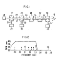
- the Klystron comprises an electron gun 10 (shown functionally) for injecting a linear electron beam 12 thru a succession of interaction cavities 18, 24, 28, 32, 36 into a final collector 16.
- the first cavity 18 is driven by an external signal generator 20 via a transmission line 21 to impress the input signal on beam 12.
- beam 12 travels down a first drift tube 22 to a second cavity 24, thence thru a succession of drift tubes 26, 30, 34 of generally decreasing lengths between successive cavities 28, 32, 36.
- Cavities 24, 28, 32 are called “floating" cavities because they have no coupling to external wave-interaction circuits.
- one such as 24 or more may be coupled to an external dissipative load 40 via a transmission line 29 to decrease its Q and hence increase the inherent bandwidth.
- the final, or "output" cavity 36 is coupled via transmission line 42, such as a hollow waveguide, to the useful microwave load 44, such as an antenna.
- output cavity 36 is tuned to the center of the operating frequency band.
- Input cavity 18 may be tuned near the lower edge of the band or, in some embodiments, to a frequency at or near the center.
- Floating cavities 24, 28, 32 are preferably tuned to frequencies successively higher than input cavity 18 or subsequent cavity 24, whichever is tuned lowest. However, for special applications, one or more may be tuned outside this sequence.
- FIG. 2 is a calculated graph of the gain vs. frequency of a 12-cavity klystron embodying the invention.
- the resonant frequencies of the sequence of cavities 1-12 are indicated on the abscissa.
- a direct comparison of the result with the prior art is not meaningful because the prior art is so diversified.
- Another advantage of the invention is that the improved gain-bandwidth may be obtained in an over- all tube length at most no longer than prior-art schemes.
- FIG. 3 is a schematic diagram of a somewhat different embodiment having only four cavities 18', 24', 28', 36'.
- the functional arrangement is the same as in FIG. 1.
- the tuning and drift-length sequences should be just as described above because no additional cavities are available to mitigate the zeros due to other cavities.
- Another advantage of the invention is that the improved gain-bandwidth may be obtained in an over- all tube length at most no longer than prior-art schemes.
Landscapes
- Microwave Tubes (AREA)
- Microwave Amplifiers (AREA)
Description
- The invention pertains to multi-cavity klystron amplifier tubes such as used in high-power microwave transmitters for radar and communications where an appreciable band of frequencies must be amplified uniformly.
- It is known that the efficiency of a klystron amplifier tube can be improved by providing a "floating" cavity (no external wave connections) upstream of the output cavity. This penultimate cavity is at a crictical, rather short distance upstream of the output and is tuned to a resonant frequency higher than the operating frequency so that its impedance is inductive. In that way, the beam bunching produced by the penultimate cavity is in phase with the already existing bunching entering it.
- To increase the gain, it is customary to add other floating cavities between the input and penultimate cavities. For maximum gain, these have been tuned to the signal frequency. However, they sharply reduce the overall frequency bandwidth, by a combination of effects. First, there is the cumulative sharpening due to a sequence of circuits tuned "synchronously" to the same frequency, as in any simple multi-stage amplifier.
- When increased bandwidth is needed, the prior art approach was to add more floating cavities and stagger their resonance frequencies. This is analogous to bandpass filters and conventional amplifiers, for which design procedures are well known. However, a klystron is not like a coupled-cavity filter, or an intermediate-frequency amplifier with only sequential coupling between circuits. In a klystron there is a foward-only coupling by the electron stream from each cavity to all other cavities downstream from it. This makes the overall response characteristic very complicated, and its mathematical calculation is best done by computer simulation. A simplified concept is to consider just three cavities: relatively broad-band externally loaded input and output cavities tuned to the same frequency and a single, unloaded intermediate cavity tuned inside their passband. As described above under efficiency, for a transmitted frequency below the resonance of the intermediate cavity, the velocity modulation produced by it is in phase with the modulation entering it so the gain is enhanced. However, for a frequency above its resonance, the intermediate cavity appears capacitive and the modulation produced by it tends to cancel the fed-thru modulation from the input. As the frequency increases the capacitive impedance of the floating cavity decreases so its internally produced modulation decreases. For a certain frequency it becomes equal and opposite to the fed-thru modulation and a zero point in gain is reached.
- The cumulative result of these kinds of effects is to make the response of a multi-cavity stagger- tuned klystron very complex.
- Many empirical and quasi-theorectical tuning programs have been devised. These involve choices of resonant frequencies, cavity Q's and intercavity drift lengths. A few examples will suffice.
- U.S. Patent No. 3,210,593 issued October 5, 1965 to C.E. Blinn and G. Caryotakis describes a choice of resonant frequencies and cavity Q's.
- U.S. Patent No. 3,249,794 issued May 3, 1966 to A. Staprans and G. Caryotakis describes tuning the floating driver cavities to progfessively higher frequencies, with Q's decreasing and then rising.
- In most of this prior art, no attention was given to the drift lengths between cavities. From simple klystron theory it was known that the greatest gain per stage required the space-charge wavelength between cavities be approaching one-quarter wave. To minimize overall the tube lengths the drift spaces were sometimes made somewhat shorter, but their effect on bandpass characteristics was seldom considered an important design characteristic.
- A recent development in klystron gain-bandwidth was described at the May 1986 Microwave Power Tube Conference sponsored by the Institute of Electrical and Electronic Engineers. As described in the published abstract and the notes published in the June 1986 issue of Microwave Journal, V. 29, No. 6,
page 32, the improvement was to use a pair of intermediate cavities tuned to the same frequency and spaced very closely together along the beam. The main effect was to obliterate one of the zeros without lengthening the over-all tube structure. A disadvantage of Symons' tube is that to get the two cavity gaps very close together along the beam can entail locating the gaps off-center in the adjacent cavities. This lowers the inherent characteristic impedance (R/Q) of the cavities, thus raising the operating Q for a desired interaction impedance. The result is to make the frequency response less flat and also more sensitive to manufacturing tolerances and environmental conditions. - US-
A 3 819 977 discloses a klystron amplifier tube with a beam-interaction structure comprising an input cavity adapted to couple to an external signal source, an output cavity adapted to couple to an external load and a number of floating cavities between the input and the output cavities. The floating cavities are designed to enhance the electron bunching in a central cavity and in one embodiment the floating cavities are drift spaces whose normalized lenghts are a maximum at the second space progressively reducing through the first, third and fourth spaces. - The present invention improves upon this amplifier by a consecutive sequence of at least three floating cavities which have progressively higher resonant frequencies and interaction gaps separated from the interaction gap of the immediately preceding cavity by progressively shorter drift spaces.
- An example of the invention will now be described with reference to the accompanying drawings in which:-
- Fig. 1 is a schematic diagram of a Klystron embodying the invention and,
- Fig. 2 is a sketch of a typical response of the tube of Fig. 1.
- The essence of the invention is the concept that improved gain-bandwith can be obtained by tuning the floating cavities to successively higher frequencies while successively decreasing the drift lenghts between them. It is recognized that the tuning program can be applied to conventionally constructed tubes. However, to obtain optimum performance the tube must additionally incorporate construction features as illustrated by Fig. 1.
- The Klystron comprises an electron gun 10 (shown functionally) for injecting a
linear electron beam 12 thru a succession ofinteraction cavities final collector 16. - The
first cavity 18 is driven by anexternal signal generator 20 via atransmission line 21 to impress the input signal onbeam 12. After passage thruinput cavity 18beam 12 travels down a first drift tube 22 to asecond cavity 24, thence thru a succession ofdrift tubes successive cavities Cavities external dissipative load 40 via atransmission line 29 to decrease its Q and hence increase the inherent bandwidth. The final, or "output"cavity 36 is coupled viatransmission line 42, such as a hollow waveguide, to theuseful microwave load 44, such as an antenna. - In the preferred embodiment,
output cavity 36 is tuned to the center of the operating frequency band.Input cavity 18 may be tuned near the lower edge of the band or, in some embodiments, to a frequency at or near the center. Floatingcavities input cavity 18 orsubsequent cavity 24, whichever is tuned lowest. However, for special applications, one or more may be tuned outside this sequence. - FIG. 2 is a calculated graph of the gain vs. frequency of a 12-cavity klystron embodying the invention. The resonant frequencies of the sequence of cavities 1-12 are indicated on the abscissa. A direct comparison of the result with the prior art is not meaningful because the prior art is so diversified.
- Another advantage of the invention is that the improved gain-bandwidth may be obtained in an over- all tube length at most no longer than prior-art schemes.
- FIG. 3 is a schematic diagram of a somewhat different embodiment having only four cavities 18', 24', 28', 36'. The functional arrangement is the same as in FIG. 1. With four cavities the tuning and drift-length sequences should be just as described above because no additional cavities are available to mitigate the zeros due to other cavities.
- It will be obvious to those skilled in the art that variations in the embodiments may be made within the true scope of the invention. The invention is to be limited only by the following claims and their legal equivalents.
- Another advantage of the invention is that the improved gain-bandwidth may be obtained in an over- all tube length at most no longer than prior-art schemes.
Claims (6)
Applications Claiming Priority (2)
| Application Number | Priority Date | Filing Date | Title |
|---|---|---|---|
| US06/932,806 US4764710A (en) | 1986-11-19 | 1986-11-19 | High-efficiency broad-band klystron |
| US932806 | 1986-11-19 |
Publications (3)
| Publication Number | Publication Date |
|---|---|
| EP0268405A2 EP0268405A2 (en) | 1988-05-25 |
| EP0268405A3 EP0268405A3 (en) | 1988-07-13 |
| EP0268405B1 true EP0268405B1 (en) | 1990-08-08 |
Family
ID=25462969
Family Applications (1)
| Application Number | Title | Priority Date | Filing Date |
|---|---|---|---|
| EP87309793A Expired EP0268405B1 (en) | 1986-11-19 | 1987-11-05 | High-efficiency broad-band klystron |
Country Status (4)
| Country | Link |
|---|---|
| US (1) | US4764710A (en) |
| EP (1) | EP0268405B1 (en) |
| JP (1) | JP2648736B2 (en) |
| DE (1) | DE3764240D1 (en) |
Families Citing this family (5)
| Publication number | Priority date | Publication date | Assignee | Title |
|---|---|---|---|---|
| US5521551A (en) * | 1994-11-21 | 1996-05-28 | Ferguson; Patrick E. | Method for suppressing second and higher harmonic power generation in klystrons |
| WO1997027610A1 (en) * | 1996-01-23 | 1997-07-31 | C. International Business Corporation Limited (C.Ibc Ltd.) | Device for grouping electron bunches |
| US8559894B2 (en) * | 2011-09-01 | 2013-10-15 | Baron Services, Inc. | Klystron transmitter |
| US9697978B2 (en) * | 2015-06-17 | 2017-07-04 | The Board Of Trustees Of The Leland Stanford Junior University | Multi-frequency klystron designed for high efficiency |
| JP7032222B2 (en) * | 2018-04-18 | 2022-03-08 | キヤノン電子管デバイス株式会社 | Klystron |
Family Cites Families (11)
| Publication number | Priority date | Publication date | Assignee | Title |
|---|---|---|---|---|
| US2605444A (en) * | 1948-08-17 | 1952-07-29 | Westinghouse Electric Corp | Multichannel frequency selector and amplifier |
| US3195007A (en) * | 1960-10-28 | 1965-07-13 | Litton Prec Products Inc | Stagger-tuned klystron with cavities resonant outside passband |
| US3622834A (en) * | 1970-04-15 | 1971-11-23 | Varian Associates | High-efficiency velocity modulation tube employing harmonic prebunching |
| JPS533225B2 (en) * | 1972-04-18 | 1978-02-04 | ||
| US3942066A (en) * | 1972-10-25 | 1976-03-02 | Nippon Electric Company Limited | Velocity modulation tube including a high resonance-frequency floating prebuncher having a q-value lower than a low resonance-frequency input cavity |
| JPS535111B2 (en) * | 1972-12-06 | 1978-02-23 | ||
| GB1449745A (en) * | 1973-06-22 | 1976-09-15 | Nippon Electric Co | Microwave tubes |
| JPS5169355A (en) * | 1974-12-06 | 1976-06-15 | Nippon Electric Co | Kokoritsu 4 kudosokudohenchokan |
| JPS51115768A (en) * | 1975-04-03 | 1976-10-12 | Nec Corp | Wide-band speed modurated tube |
| EP0008896B1 (en) * | 1978-09-06 | 1982-08-04 | Thorn Emi-Varian Limited | An output section for a microwave amplifier, a microwave amplifier and a circuit for use in a microwave amplifier |
| JPS58186138A (en) * | 1982-04-26 | 1983-10-31 | Toshiba Corp | Klystron device |
-
1986
- 1986-11-19 US US06/932,806 patent/US4764710A/en not_active Expired - Lifetime
-
1987
- 1987-11-05 EP EP87309793A patent/EP0268405B1/en not_active Expired
- 1987-11-05 DE DE8787309793T patent/DE3764240D1/en not_active Expired - Lifetime
- 1987-11-16 JP JP62287596A patent/JP2648736B2/en not_active Expired - Fee Related
Also Published As
| Publication number | Publication date |
|---|---|
| EP0268405A3 (en) | 1988-07-13 |
| EP0268405A2 (en) | 1988-05-25 |
| DE3764240D1 (en) | 1990-09-13 |
| JPS63284737A (en) | 1988-11-22 |
| US4764710A (en) | 1988-08-16 |
| JP2648736B2 (en) | 1997-09-03 |
Similar Documents
| Publication | Publication Date | Title |
|---|---|---|
| US4371853A (en) | Strip-line resonator and a band pass filter having the same | |
| US5066933A (en) | Band-pass filter | |
| EP0008896B1 (en) | An output section for a microwave amplifier, a microwave amplifier and a circuit for use in a microwave amplifier | |
| EP0417205B1 (en) | High performance extended interaction output circuit | |
| US5469022A (en) | Extended interaction output circuit using modified disk-loaded waveguide | |
| US4764710A (en) | High-efficiency broad-band klystron | |
| US2746036A (en) | Device for coupling between free space and an electron stream | |
| US5406234A (en) | Tunable microwave filter apparatus having a notch resonator | |
| US3365607A (en) | Electron discharge device | |
| US2916658A (en) | Backward wave tube | |
| US2960658A (en) | Microwave amplifiers | |
| US3576460A (en) | Impedance match for periodic microwave circuits and tubes using same | |
| US8143973B2 (en) | Cavity filter coupling system | |
| US4019089A (en) | Wideband multi-cavity velocity modulation tube | |
| US4752753A (en) | Coaxial waveguide band reject filter | |
| US3538377A (en) | Traveling wave amplifier having an upstream wave reflective gain control element | |
| US4800322A (en) | Broadband klystron cavity arrangement | |
| CN111180296A (en) | Broadband extension interaction amplifier circuit | |
| US2958001A (en) | Parametric amplifier | |
| US2720610A (en) | Noise reducing travelling-wave tube | |
| CA1086862A (en) | Lossless traveling wave booster tube | |
| RU2714508C1 (en) | Miniature multi-beam klystron | |
| US2807784A (en) | Coupling and matching device for external circuits of a traveling wave tube | |
| US6483243B1 (en) | Multiband travelling wave tube of reduced length capable of high power functioning | |
| US3974417A (en) | Four-cavity velocity modulation tube |
Legal Events
| Date | Code | Title | Description |
|---|---|---|---|
| PUAI | Public reference made under article 153(3) epc to a published international application that has entered the european phase |
Free format text: ORIGINAL CODE: 0009012 |
|
| PUAL | Search report despatched |
Free format text: ORIGINAL CODE: 0009013 |
|
| AK | Designated contracting states |
Kind code of ref document: A2 Designated state(s): BE DE FR GB IT NL |
|
| AK | Designated contracting states |
Kind code of ref document: A3 Designated state(s): BE DE FR GB IT NL |
|
| 17P | Request for examination filed |
Effective date: 19880930 |
|
| 17Q | First examination report despatched |
Effective date: 19890928 |
|
| GRAA | (expected) grant |
Free format text: ORIGINAL CODE: 0009210 |
|
| AK | Designated contracting states |
Kind code of ref document: B1 Designated state(s): BE DE FR GB IT NL |
|
| REF | Corresponds to: |
Ref document number: 3764240 Country of ref document: DE Date of ref document: 19900913 |
|
| ET | Fr: translation filed | ||
| ITF | It: translation for a ep patent filed | ||
| PLBE | No opposition filed within time limit |
Free format text: ORIGINAL CODE: 0009261 |
|
| STAA | Information on the status of an ep patent application or granted ep patent |
Free format text: STATUS: NO OPPOSITION FILED WITHIN TIME LIMIT |
|
| 26N | No opposition filed | ||
| ITTA | It: last paid annual fee | ||
| PGFP | Annual fee paid to national office [announced via postgrant information from national office to epo] |
Ref country code: NL Payment date: 19911130 Year of fee payment: 5 |
|
| PGFP | Annual fee paid to national office [announced via postgrant information from national office to epo] |
Ref country code: GB Payment date: 19921026 Year of fee payment: 6 |
|
| PGFP | Annual fee paid to national office [announced via postgrant information from national office to epo] |
Ref country code: DE Payment date: 19921123 Year of fee payment: 6 |
|
| PGFP | Annual fee paid to national office [announced via postgrant information from national office to epo] |
Ref country code: BE Payment date: 19921211 Year of fee payment: 6 |
|
| PG25 | Lapsed in a contracting state [announced via postgrant information from national office to epo] |
Ref country code: NL Effective date: 19930601 |
|
| NLV4 | Nl: lapsed or anulled due to non-payment of the annual fee | ||
| PG25 | Lapsed in a contracting state [announced via postgrant information from national office to epo] |
Ref country code: GB Effective date: 19931105 |
|
| PG25 | Lapsed in a contracting state [announced via postgrant information from national office to epo] |
Ref country code: BE Effective date: 19931130 |
|
| BERE | Be: lapsed |
Owner name: VARIAN ASSOCIATES INC. Effective date: 19931130 |
|
| GBPC | Gb: european patent ceased through non-payment of renewal fee |
Effective date: 19931105 |
|
| PG25 | Lapsed in a contracting state [announced via postgrant information from national office to epo] |
Ref country code: DE Effective date: 19940802 |
|
| REG | Reference to a national code |
Ref country code: FR Ref legal event code: TP |
|
| PGFP | Annual fee paid to national office [announced via postgrant information from national office to epo] |
Ref country code: FR Payment date: 19961021 Year of fee payment: 10 |
|
| PG25 | Lapsed in a contracting state [announced via postgrant information from national office to epo] |
Ref country code: FR Free format text: THE PATENT HAS BEEN ANNULLED BY A DECISION OF A NATIONAL AUTHORITY Effective date: 19971130 |
|
| REG | Reference to a national code |
Ref country code: FR Ref legal event code: ST |
|
| PG25 | Lapsed in a contracting state [announced via postgrant information from national office to epo] |
Ref country code: IT Free format text: LAPSE BECAUSE OF NON-PAYMENT OF DUE FEES;WARNING: LAPSES OF ITALIAN PATENTS WITH EFFECTIVE DATE BEFORE 2007 MAY HAVE OCCURRED AT ANY TIME BEFORE 2007. THE CORRECT EFFECTIVE DATE MAY BE DIFFERENT FROM THE ONE RECORDED. Effective date: 20051105 |