EP0268230B1 - Silicon carbide capillaries - Google Patents
Silicon carbide capillaries Download PDFInfo
- Publication number
- EP0268230B1 EP0268230B1 EP19870116794 EP87116794A EP0268230B1 EP 0268230 B1 EP0268230 B1 EP 0268230B1 EP 19870116794 EP19870116794 EP 19870116794 EP 87116794 A EP87116794 A EP 87116794A EP 0268230 B1 EP0268230 B1 EP 0268230B1
- Authority
- EP
- European Patent Office
- Prior art keywords
- capillary
- substrate
- coating
- silicon carbide
- wire
- Prior art date
- Legal status (The legal status is an assumption and is not a legal conclusion. Google has not performed a legal analysis and makes no representation as to the accuracy of the status listed.)
- Expired - Lifetime
Links
Images


Classifications
-
- H—ELECTRICITY
- H10—SEMICONDUCTOR DEVICES; ELECTRIC SOLID-STATE DEVICES NOT OTHERWISE PROVIDED FOR
- H10W—GENERIC PACKAGES, INTERCONNECTIONS, CONNECTORS OR OTHER CONSTRUCTIONAL DETAILS OF DEVICES COVERED BY CLASS H10
- H10W72/00—Interconnections or connectors in packages
- H10W72/071—Connecting or disconnecting
- H10W72/0711—Apparatus therefor
-
- B—PERFORMING OPERATIONS; TRANSPORTING
- B23—MACHINE TOOLS; METAL-WORKING NOT OTHERWISE PROVIDED FOR
- B23K—SOLDERING OR UNSOLDERING; WELDING; CLADDING OR PLATING BY SOLDERING OR WELDING; CUTTING BY APPLYING HEAT LOCALLY, e.g. FLAME CUTTING; WORKING BY LASER BEAM
- B23K20/00—Non-electric welding by applying impact or other pressure, with or without the application of heat, e.g. cladding or plating
- B23K20/002—Non-electric welding by applying impact or other pressure, with or without the application of heat, e.g. cladding or plating specially adapted for particular articles or work
- B23K20/004—Wire welding
- B23K20/005—Capillary welding
- B23K20/007—Ball bonding
-
- C—CHEMISTRY; METALLURGY
- C23—COATING METALLIC MATERIAL; COATING MATERIAL WITH METALLIC MATERIAL; CHEMICAL SURFACE TREATMENT; DIFFUSION TREATMENT OF METALLIC MATERIAL; COATING BY VACUUM EVAPORATION, BY SPUTTERING, BY ION IMPLANTATION OR BY CHEMICAL VAPOUR DEPOSITION, IN GENERAL; INHIBITING CORROSION OF METALLIC MATERIAL OR INCRUSTATION IN GENERAL
- C23C—COATING METALLIC MATERIAL; COATING MATERIAL WITH METALLIC MATERIAL; SURFACE TREATMENT OF METALLIC MATERIAL BY DIFFUSION INTO THE SURFACE, BY CHEMICAL CONVERSION OR SUBSTITUTION; COATING BY VACUUM EVAPORATION, BY SPUTTERING, BY ION IMPLANTATION OR BY CHEMICAL VAPOUR DEPOSITION, IN GENERAL
- C23C16/00—Chemical coating by decomposition of gaseous compounds, without leaving reaction products of surface material in the coating, i.e. chemical vapour deposition [CVD] processes
- C23C16/01—Chemical coating by decomposition of gaseous compounds, without leaving reaction products of surface material in the coating, i.e. chemical vapour deposition [CVD] processes on temporary substrates, e.g. substrates subsequently removed by etching
-
- H—ELECTRICITY
- H10—SEMICONDUCTOR DEVICES; ELECTRIC SOLID-STATE DEVICES NOT OTHERWISE PROVIDED FOR
- H10W—GENERIC PACKAGES, INTERCONNECTIONS, CONNECTORS OR OTHER CONSTRUCTIONAL DETAILS OF DEVICES COVERED BY CLASS H10
- H10W72/00—Interconnections or connectors in packages
- H10W72/01—Manufacture or treatment
- H10W72/015—Manufacture or treatment of bond wires
- H10W72/01551—Changing the shapes of bond wires
-
- H—ELECTRICITY
- H10—SEMICONDUCTOR DEVICES; ELECTRIC SOLID-STATE DEVICES NOT OTHERWISE PROVIDED FOR
- H10W—GENERIC PACKAGES, INTERCONNECTIONS, CONNECTORS OR OTHER CONSTRUCTIONAL DETAILS OF DEVICES COVERED BY CLASS H10
- H10W72/00—Interconnections or connectors in packages
- H10W72/071—Connecting or disconnecting
- H10W72/0711—Apparatus therefor
- H10W72/07141—Means for applying energy, e.g. ovens or lasers
-
- H—ELECTRICITY
- H10—SEMICONDUCTOR DEVICES; ELECTRIC SOLID-STATE DEVICES NOT OTHERWISE PROVIDED FOR
- H10W—GENERIC PACKAGES, INTERCONNECTIONS, CONNECTORS OR OTHER CONSTRUCTIONAL DETAILS OF DEVICES COVERED BY CLASS H10
- H10W72/00—Interconnections or connectors in packages
- H10W72/071—Connecting or disconnecting
- H10W72/075—Connecting or disconnecting of bond wires
- H10W72/07511—Treating the bonding area before connecting, e.g. by applying flux or cleaning
-
- H—ELECTRICITY
- H10—SEMICONDUCTOR DEVICES; ELECTRIC SOLID-STATE DEVICES NOT OTHERWISE PROVIDED FOR
- H10W—GENERIC PACKAGES, INTERCONNECTIONS, CONNECTORS OR OTHER CONSTRUCTIONAL DETAILS OF DEVICES COVERED BY CLASS H10
- H10W72/00—Interconnections or connectors in packages
- H10W72/071—Connecting or disconnecting
- H10W72/075—Connecting or disconnecting of bond wires
- H10W72/07531—Techniques
- H10W72/07532—Compression bonding, e.g. thermocompression bonding
-
- H—ELECTRICITY
- H10—SEMICONDUCTOR DEVICES; ELECTRIC SOLID-STATE DEVICES NOT OTHERWISE PROVIDED FOR
- H10W—GENERIC PACKAGES, INTERCONNECTIONS, CONNECTORS OR OTHER CONSTRUCTIONAL DETAILS OF DEVICES COVERED BY CLASS H10
- H10W72/00—Interconnections or connectors in packages
- H10W72/071—Connecting or disconnecting
- H10W72/075—Connecting or disconnecting of bond wires
- H10W72/07531—Techniques
- H10W72/07532—Compression bonding, e.g. thermocompression bonding
- H10W72/07533—Ultrasonic bonding, e.g. thermosonic bonding
-
- H—ELECTRICITY
- H10—SEMICONDUCTOR DEVICES; ELECTRIC SOLID-STATE DEVICES NOT OTHERWISE PROVIDED FOR
- H10W—GENERIC PACKAGES, INTERCONNECTIONS, CONNECTORS OR OTHER CONSTRUCTIONAL DETAILS OF DEVICES COVERED BY CLASS H10
- H10W72/00—Interconnections or connectors in packages
- H10W72/50—Bond wires
- H10W72/551—Materials of bond wires
- H10W72/552—Materials of bond wires comprising metals or metalloids, e.g. silver
-
- H—ELECTRICITY
- H10—SEMICONDUCTOR DEVICES; ELECTRIC SOLID-STATE DEVICES NOT OTHERWISE PROVIDED FOR
- H10W—GENERIC PACKAGES, INTERCONNECTIONS, CONNECTORS OR OTHER CONSTRUCTIONAL DETAILS OF DEVICES COVERED BY CLASS H10
- H10W72/00—Interconnections or connectors in packages
- H10W72/50—Bond wires
- H10W72/551—Materials of bond wires
- H10W72/552—Materials of bond wires comprising metals or metalloids, e.g. silver
- H10W72/5522—Materials of bond wires comprising metals or metalloids, e.g. silver comprising gold [Au]
-
- H—ELECTRICITY
- H10—SEMICONDUCTOR DEVICES; ELECTRIC SOLID-STATE DEVICES NOT OTHERWISE PROVIDED FOR
- H10W—GENERIC PACKAGES, INTERCONNECTIONS, CONNECTORS OR OTHER CONSTRUCTIONAL DETAILS OF DEVICES COVERED BY CLASS H10
- H10W72/00—Interconnections or connectors in packages
- H10W72/50—Bond wires
- H10W72/551—Materials of bond wires
- H10W72/552—Materials of bond wires comprising metals or metalloids, e.g. silver
- H10W72/5524—Materials of bond wires comprising metals or metalloids, e.g. silver comprising aluminium [Al]
-
- Y—GENERAL TAGGING OF NEW TECHNOLOGICAL DEVELOPMENTS; GENERAL TAGGING OF CROSS-SECTIONAL TECHNOLOGIES SPANNING OVER SEVERAL SECTIONS OF THE IPC; TECHNICAL SUBJECTS COVERED BY FORMER USPC CROSS-REFERENCE ART COLLECTIONS [XRACs] AND DIGESTS
- Y10—TECHNICAL SUBJECTS COVERED BY FORMER USPC
- Y10T—TECHNICAL SUBJECTS COVERED BY FORMER US CLASSIFICATION
- Y10T428/00—Stock material or miscellaneous articles
- Y10T428/13—Hollow or container type article [e.g., tube, vase, etc.]
- Y10T428/131—Glass, ceramic, or sintered, fused, fired, or calcined metal oxide or metal carbide containing [e.g., porcelain, brick, cement, etc.]
Definitions
- This invention relates to capillaries for ball bonding fine electrical conductor wire to electrical components and more particularly, to silicon carbide capillaries having particular application in thermosonic bonding tools, a method for making the same by chemical vapor deposition (CVD) techniques and an apparatus for incorporating such capillaries.
- CVD chemical vapor deposition
- ICs silicon integrated circuits
- One example of the need for such an improvement is to increase the wear life of the capillaries or weld tip guides used in the wire ball bonding operation of the IC fabrication process.
- a clean, bare fine electrical conductor such as gold, aluminum or silver is attached between a bonding pad on the IC ship and pins on the chip support.
- the fine electrical on- ductor wire of filament usually about 0.018 to 0.13 mm (0.7 to 5 mils) in thickness (0.0007 in. to 0.005 in.), is fed through the bonding tool known as the capillary.
- thermosonic bonding In the case of the currently most popular bondingmeans, i.e. thermosonic bonding, the capillary is held in an ultrasonic transducer horn, a ball is formed at the tip end of the capillary by melting the wire using an electrical spark, and the ball is bonded between the bonding pad and pins by a combination of thermocompression and ultrasonic techniques; see Microelectron Manufacturing and Testing, August 1984, pages 53-54.
- Thermosonic bonding is done in bonding machines which include relatively simple manually operated types to more advanced high speed fully automatic wire bonders, which include microprocessors for pattern recognition and maintaining bonding schedules; see the product brochure for the Model 2460 thermosonic gold ball bonding machine by Hughes Aircraft Company.
- Alumina capillaries are formed by a process which comprises mixing an aqueous slurry of alumina with a proper binder, molding the mixture into a compact shape over a mold pin and sintering the alumina to form the finished product. It is the binders used in the forming process that contribute to failures of the capillaries during use.
- CDV chemical vapor deposition
- any suitable highly refractory hard material having a Vickers mi- crohardness in excess of about 3.9 GN/m 2 (400 kg/mm 2 ) can be used to produce the capillaries
- particularly suitable materials include tungsten, rhenium and molybdenum, and tantalum and alloys thereof, such as tungsten-carbide, tungsten-molybdenum and tungsten-rhenium, as well as tantalum-carbide and columbium-carbide.
- Such capillaries are unsuitable in thermocompression and ultrasonic bonders which use electric generators for producing the hot ball and thus, require resistivities of no less than 0.1 ohm-cm. No suggestion is made in this patent of preparing silicon carbide capillaries by CVD techniques and hence, the patentees had no recognition of the problems which are associated with preparing such capillaires and which had to be overcome to produce CVD silicon carbide capillaries.
- capillaries from relatively low melting point cementitious metals, such as cobalt, titanium and nickel. Such capillaries must be sintered using binder materials which have the disadvantage of reacting with the fine wire of the bonding operation causing loss of bond strength. Electrochemical deposition methods for forming capillaries have been used to produce nickel, copper and iron capillaries which are all unsuitable because these metals react with the fine wire.
- the present invention is directed to an article of manufacture comprising a capillary having an axially extending passage terminating in a relatively small diameter guide opening at an end thereof through which a fine, electrical conductor wire is adapted to pass and which is for engaging a hot ball on the wire by thermocompression or thermosonic means.
- the resistivity of the resulting silicon carbide coated capillary is at least 1 ohm cm, a uniform Vickers hardness of gre- aer than 27.5 GN/m 2 (2800 kg/mm 2 ), a density of at least 3.15 gm/cm 3 , a TSR of at least 190 and a fracture toughness of at least 4 Ki c.
- the capillary is made by a ethod comprising: chemical vapor depositing a substantially smooth outer refractory coating onto a substrate having a tapered end by introducing a gaseous mixture capable of depositing a coating onto the substrate; machining the resulting coating to the desired overall length;
- the outer coating is silicon carbide deposited by the chemical vapor deposition step in the absence of oxygen or oxygen containing compound, that the rate of depposition of silicon carbide onto the substrate is controlled wtihin the range of about 0.0025 to 0.076 mm/h (1 to 3 mils/h) at a temperature in the range of about 1200 ° to 1400°C, and that the steps of machining the resulting silicon carbide coated substrate to the desired length and machining the tapered end of the coating to the desired diameter take place prior to the step of removing the substrate from the outer silicon carbide coating.
- the method of the present invention produces a substantially smooth, uniform, hard, fine-grained coating of silicon carbide, which is sufficiently high in electrical resistivity that the resulting capillary does not arc when subjected to an electric spark generator during EFO bonding.
- the end of the fine wire to be bonded is positioned just below the bonding tip by passing the wire through the wire-guide hole in the tip.
- the nonconductive nature of the silicon carbide is such that on applying electric energy, a spark of high density plasma is created below the bonding tip encircling the wire which causes the wire to melt to form a ball of molten metal.
- the bonding tip exerts a load on the tip which causes the molten ball to be forced against the chip pad to produce the ball bond.
- the bonder reverses direction sliding up over the wire and moves over the substrate pad as the wire is fed out of the capillary forming a wire loop.
- the bonder produces a second bond on the substrate pad or lead in the same manner.
- the bonder is raised and the wire is broken at the point of the second bond to complete the circuit between the chip and the substrate.
- the spark does not arc across the guide opening of the capillary which would occur if capillaries produced by the prior art CVD processes were used.
- capillaries of the present invention exhibit substantially increased resistance to thermal shock over standard alumina capillaries.
- the CVD silicon carbide capillaries of the present invention have been found to have nine times the wear life of alumina capillaries in the EFO bonding process and, hence, have very great market appeal.
- the silicon-containing gas used to form the silicon carbide coating can be selected from the group consisting of silicon tetrachloride, silane, dichlorosilane, trichlorosilane, methyl trichlorosilane and dimethyl dichlorosilane. If silicon tetrachloride, silane, dichlorosilane or trichlorosilane is used, it is necessary to supply a source of carbon to produce silicon carbide.
- the source of carbon can be any hydrocarbon, preferably low molecular weight aliphatic hydrocarbons such as paraffins, alkenes, and alkynes having one to six carbon atoms, and aromatics and other hydrocarbons having one to six carbon atoms which do not contain oxygen. Particularly suitable examples include methane, ethane, propane, butane, methylene, ethylene, propylene, butylene, acetylene and benzene.
- a typical bonding apparatus for bonding a fine electrical conductor wire to an electrical component which uses capillaries of the present invention comprises:
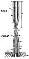
- Fig. 1 illustrates the shape of a conventional form of capillary 1 including tip 2 comprises an axially extending passage 3 which includes an upper cylindrical portion 4 communicating with an inwardly tapered conical portion 5 which in turn communicates with a terminal cylindrical guide opening 6.
- the inner surfaces of apssage 3 must be smooth so as not to interfere with or scratch the surface of the fine wire or filament which is guided through capillary 1 with precision.
- Guide opening 6 is of practically capillary diameter ranging from about 0.025 to 0.18 mm (0.001 inch to 0.007 inch) for fine wire 7 which varies in diameter from about 0.025 to 0.1 mm (0.001 to 0.004 inch).
- the dimensions of the capillary shown in Fig. 1 vary depending on the diameter of wire 7 and the particular requirements of the bonding tool. If wire 7 is 0.018 mm (0.007 inch) in diameter, guide opening 6 is approximately 0.025 mm (0.001 inch) but if a greater diameter is used, say 0.13 mm (5 mils) the diameter of opening 6 is about 0.18 mm (7 mils).
- the length of a typical capillary is about 12.7 mm ( 1 / 2 inch) or sufficiently long so that wire 7 can be guided through capillary 1 without kinking and must be sufficiently narrow so that capillary tip 2 adjacent to guide opening 6 can engage molten ball 8 formed on the wire to join the pad on the circuit with the pad on the chip carrier.
- the prior art alumina capillaries were limited to about 12.7 mm ( 1 / 2 inch) in EFO bonding because of their thermal shock fracture resistance.
- the silicon carbide capillaries of the present invention are not length limited because of their greater thermal shock resistance. This permits the capillaries of this invention to be used in deep access bonding which require longer capillaries.
- the length of conical section 4 is approximately 3.2 mm ( 1 / 8 inch).
- the inside diameter of cylindrical portion 3 being about 1.6 mm ( 1 f 16 inch) in diameter.
- Fig. 2 illustrates mandrel 100 upon which has been deposited silicon carbide coating 102 to form CVD coated mandrel 104.
- Mandrel 100 comprises a material which can be easily removed from coated mandrel 104 to form passage 3 of capillary 1 of Fig. 1.
- a plurality of mandrels 100 are respectively mounted in a plurality of tapered recesses 106 within support tray 108 and tray 108 of mandrels 100 are then subjected to CVD coating in the manner descirbed below in connection with a description of FIG. 3.
- Tapered projection 110 of mandrel 100 forms inwardly- tapered conical portion 5 and guide opening 6 of capillary 1.
- Cylindrical portion 112 forms cylindrical portion 4 as shown in FIG. 1.
- continuous, solid integral coating 102 of silicon carbide is molecularly bonded to mandrel 100 to form capillary 1 of the desired wall thickness which is sufficient to allow subsequent exterior machining operations to suit the particular bonding tool. It has been found that a suitable thickness of coating 102 ranges from about 0.01 to 0.03 inch and preferably about 0.02 inch.
- silicon carbide coated mandrel 102 is removed from recess 106 in support tray 108. Without the countersunk recess, (see Fig. 6) a bridge of CVD silicon carbide will form (not shown) between the lower end of mandrel 100 and the upper surface of support tray 108 and must be broken adjacent coated end 118 before coated mandrel 104 can be removed from tray 108.
- Coated portion 120 at or adjacent to the end of tapered portion 112 is trimmed off by drilling, cutting, grinding or other machining operation to give capillary guide opening 6 of the proper diameter when mandrel 100 is removed.
- Coated mandrel 104 is placed in a jig (not shown) with coated end 118 in the upright position and end 118 is cut, ground or otherwise machined by suitable means so that capillary 1 will have the desired length.
- the composition of mandrel 100 can comprise graphite, tungsten, molybdenum or other suitable material which can withstand the processing condition and can easily be removed by chemical or combustion means from capillary 1 and leave a substantially smooth interior surface.
- a particularly effective composition for the mandrel is a graphite which is substantially free of additives and other extraneous matter.
- the most effective means is to burn out the graphite mandrel in a furnace at temperatures in the range of 1100° to about 1300°C. Preferably this is done by placing coated graphite mandrel 104 in a furnace and applying dry air at these temperatures for a sufficient period of time to completely burn out mandrel 100.
- the most effective means of removing the mandrel is to chemical etch.
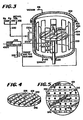
- FIGS. 3, 4 and 5 water cooled, resistance heated reactor 200 having a removable top 202 and reactor body 204 having complimentary mating flanges 205.
- Support tray 108 is mounted on extension 208 attached to rotatable shaft 210 which passes through body 204 from the bottom as shown and is rotated by suitable means (not shown).
- Support tray 108 is in turn mounted on extensions 208a, 208b and 208c.
- Mandrels 100 are located within the countersunk holes 212, which correspond to tapered recesses 106 in FIG. 2 and are described in more detail under the description of FIG. 6.
- the production capacity of reactor 200 can be increased by the addition of multiple trays 108 which are spaced from each other by means of appropriately sized extensions to provide sufficient clearance for the mandrels and to provide uniform gas flow.
- an addition support tray can be mounted on extension 208a.
- Extension 208d is shown mounted as a slip fitting on male portion 209 of extension 208c to facilitate stacking of addition trays. If extension 208d is not used, a suitable cap (not shown) is placed over male portion 209 to prevent it from being coated.
- lid 202 After mounting the mandrels, lid 202 is clamped shut, and the system is leak tested by pressurizing with nitrogen through lines 228, 230, 230a and 203b and then a vacuum is pulled by means of vacuum system 216 to remove substantially all of the air and nitrogen.
- Reactor 200 is then heated to a temperature in the range of about 1300 ° to about 1375 ° C by means of resistance heater 220 which is connected to transformer 222 for reducing the 450 volt charge to approximately 75 volts and approximately 1000 amperes.
- Temperature sensor 224 causes temperature controller 226 to modify the primary voltage on transformer 222 causing the power supplied to heater 220 to be changed, in turn changing the temperature in reactor 200 relative to the setpoint in controller 226.
- hydrogen is then introduced into reactor 200 at a flow rate dependent on the overall volume of reactor 200 in order to bring the reactor to atmospheric pressure within a reasonable period of time.
- the hydrogen is contined after the reactor reaches atmospheric pressure by exhausting it through line 236 to an exhaust scrubber (not shown) for approximately one-half hour to stabilize the reactor temperature and to further clean the mandrels 100 to make sure particulate matter and any nitrogen remaining from the previous purge has been removed from reactor 200 before introduction of the silicon- containing gases such as methyl trichlorosilane (MTS) through lines 232, 230, 230a and 230b.
- MTS methyl trichlorosilane
- FIGS. 4, 5 and 6 illustrate a preferred embodiment of the type of support tray for mandrels 100 which are designed to provide uniform flow of reactant gases during the CVD operation and to prevent any bridging of CVD coating between the upper surface of the support tray 108 and the lower end of mandrel 100.
- This latter feature permits one to remove coated mandrels 104 without shearing or fracturing them. It has been found that if the briding of CVD is allowed to build up between the latter surfaces, the removal of coated mandrels 104 from tray 108 causes stress fractures along the longitudinal axis of coating 102, thus leading to the failure of capillaries 1 in the machining step.
- FIGS. 4 and 5 show the preferred embodiment in which circular support tray 108 comprising graphite substantially free of foreign matter has a diameter such that it can easily be palced within reactor 200.
- Tray 108 is mounted on extension 208 by means of orifice 238.
- Tray 108 contains a plurality of upper grooves 240 having a depth slightly greater than one-half the thickness of tray 108, which thickness typically is approximately two inches.
- Lower grooves 242 having the same depth as those of grooves 240 are cut into tray 108 perpendicular to grooves 240 to form a plurality of square holes 244.
- Countersunk holes 212 are drilled to the desired depth equally along the spaces between upper grooves 242 as shown.
- This placement of square holes 244 and countersunk holes 212 provides for a uniform distribution of gases throughout the external surface of mandrels 100 above the surface of tray 108. This leads in turn to an even distribution of coating so that finished coated mandrels 104 have the desired coating concentricity. Coating concentricity is measured by cutting through coated mandrel 104 perpendicular to the longitudinal axis thereof and measuring the variations in the resulting cross sections.
- FIG. 6 shows tapered wall 109 of countersunk hole 212 in support tray 108 forms an angle of approximately 75° with the surface of tray 108 or 150 from the vertical axis of hole 212. This angle should be at least 10 ° and no more than 20 ° from the vertical to prevent bridging of silicon-carbide.
- the tapered portion of hole 212 is drilled to a depth of approximately 6.4 mm (0.25 inch) in the example in which mandrel 100 has a diameter of approximately 0.7 mm (0.028 inch).
- the remaining portion of hole 212 has side walls 250 parallel to the longitudinal axis of mandrel 100, a diameter of approximately 0.79 mm (0.031 inch) and a depth of approximately 12.7 mm (0.5 inch).
- Fig. 7 schematically illustrates wire bonder 258 for carrying out the thermosonically bonding process which is well known in the art for joining wire 7 from lead 260 on chip support 262, which is placed on platform 263, to pad 264 on chip 266.
- Bonder 258 housed within frame 268 comprises means 270 spaced from work station 262 for holding a spool of wire 7. Wire 7 is fed over pulley 272 through support sleeve 272 and guide means 273 for guiding wire 7 down through ultrasonic transducer 274 operably connected to transducer 276, capillary 1 and tip 2 as shown.
- Ball 8 on wire 7 is formed by the plasma generated from the electric spark 284 which is produced and passed thorugh copper electrode 286 by means of electric spark generator 290 mounted on suitable support 292. Spark 282 is directed to the end of wire 7 protruding through capillary tip 2. Because capillary 1 is substantially free of any conductive material, spark 284 does not arc across the tip which would introduce unwanted heat buildup within guide opening 6 and possibly prevent the necessary reciprocal motion of wire 7 during the bonding process.
- a block of graphite was used approximately 2 inches thick and containing 52 holes having diameters of 0.79 mm (0.031 inch) depths of about 2.54 cm (1 inch) and side walls perpendicular to the surface of the tray.
- the support tray was placed on extension 208 within reactor 200 shown in Fig. 3 and reactor lid 202 was affixed to reactor body 204 by means of bolts through flange 205.
- Vacuum grease was used on the flange surfaces to provide a vacuum type seal which was checked by pressurizing reactor 200 with nitrogen to 0.69-1.03 bar (10-15 psig) with exhaust 236 closed and then stopping the flow of nitrogen to seal off reactor 200.
- the pressure in reactor 200 was observed over a ten minute period to ensure that no more than 0.2 bar (0.3 psi) pressure was lost.
- the exhaust line 236 was then opened to allow the pressure in reactor 200 to reach atmospheric.
- the exhaust line 236 was then closed and a vacuum of 1.0 bar (29.5 in. Hg) was then pulled by means of vacuum system 216.
- Reactor 200 was heated to 1350 ° C by increasing the power supply from transformer 222 to 72 volts and 900 to 1100 amperes.
- the rate of flow of MTS is critical to achieve in the finished capillary a uniform grain size of silicon carbide. Specifically this is achieved by maintaining the silicon carbide deposition rate at approximately 2.2 mils per hour which achieves the optimum crystal growth in the shortest period of time. The lowest rate to achieve sufficient grain size is about 0.025 mm (1 mil) silicon carbide per hour and the highest practical rate is about 0.076 mm (3 mils).
- the flow of MTS was stopped and the hydrogen flow continued for 10 minutes to purge out any remaining MTS from the system. The power was shut off and the hydrogen purge continued for an additional 1 1 f 2 hours until no further glow was visible by the naked eye through a sight glass (not shown) in reactor 200.
- the coated mandrels having a coating thickness of about 0.5 mm (20 mils) were machined as discussed above and were fired in a furnace at about 1200 ° C to remove the graphite. All of the capillaries were inspected under a microscope and any surface irregularities were machined. The finished capillaries had the necessary uniform grain size and coating concentricity as measured in an electron microscope at 108 magnification.
- the capillaries had a density of 3.2 gm/cm3, a uniform Vickers hardness of 29.4 GN/m 2 (3000 kg/mm2), a tensile strength of 690 MPa (100,000 psi), modulus of elasticity of 4.8 x 10⁴ MPa /70 x 106 psi) and a coefficient of thermal expansion 4.8 x 10⁻⁶ cm/cm/ ° C.
- the capillaries were tested in thermosonic bonding devices of the type described in the Model 2460 EFO bonding machine by Hughes and found to have 9 times the wear life of alumina capillaries currently available on the market. The resistivities of the resulting capillaries were sufficiently high so that arcing did not occur during use in such bonding devices.
- the molybdenum mandrels were removed from the resulting capillaries by use of a chemical etchant comprising 4 parts of concentrated HN0 3 and 1 part concentrated H 2 S0 4 .
- the resulting capillaries had, for the most part, the same physical properties including wear life as those obtained in Example 1, except that the coating concentricity measurement identified discreet layers of silicon carbide that were build up during the separate runs referred to above.
Landscapes
- Chemical & Material Sciences (AREA)
- Engineering & Computer Science (AREA)
- Mechanical Engineering (AREA)
- General Chemical & Material Sciences (AREA)
- Chemical Kinetics & Catalysis (AREA)
- Materials Engineering (AREA)
- Metallurgy (AREA)
- Organic Chemistry (AREA)
- Chemical Vapour Deposition (AREA)
- Wire Bonding (AREA)
Description
- This invention relates to capillaries for ball bonding fine electrical conductor wire to electrical components and more particularly, to silicon carbide capillaries having particular application in thermosonic bonding tools, a method for making the same by chemical vapor deposition (CVD) techniques and an apparatus for incorporating such capillaries.
- The tremendous growth of the semiconductor industry has required suppliers of components used in the fabrication of silicon integrated circuits (ICs)s to come up with improvements in their products to increase the productivity of ICs without increasing their cost. One example of the need for such an improvement is to increase the wear life of the capillaries or weld tip guides used in the wire ball bonding operation of the IC fabrication process. In such an operation, a clean, bare fine electrical conductor such as gold, aluminum or silver is attached between a bonding pad on the IC ship and pins on the chip support. Specifically, the fine electrical on- ductor wire of filament, usually about 0.018 to 0.13 mm (0.7 to 5 mils) in thickness (0.0007 in. to 0.005 in.), is fed through the bonding tool known as the capillary. In the case of the currently most popular bondingmeans, i.e. thermosonic bonding, the capillary is held in an ultrasonic transducer horn, a ball is formed at the tip end of the capillary by melting the wire using an electrical spark, and the ball is bonded between the bonding pad and pins by a combination of thermocompression and ultrasonic techniques; see Microelectron Manufacturing and Testing, August 1984, pages 53-54. Thermosonic bonding is done in bonding machines which include relatively simple manually operated types to more advanced high speed fully automatic wire bonders, which include microprocessors for pattern recognition and maintaining bonding schedules; see the product brochure for the Model 2460 thermosonic gold ball bonding machine by Hughes Aircraft Company.
- The majority of capillaries produced in the semiconductor industry today and used in such thermosonic bonders are made of molded alumina. Such alumina capillaries are low in cost and can be discarded after use rather than having to clean or to reclaim them. However, the chief drawback of molded alumina capillaries is their relatively short wear life in high speed electronic flame off (EFO) bonding applications due to their lower resistance to thermal shock. This results in frequent replacement which lowers overall productivity during the bonding operation. Diamond, ruby and sapphire tipped capillaries have the requisite long wear life, but they do not sell at competitive prices, must be cleaned during use and should be reclaimed after their useful life.
- Alumina capillaries are formed by a process which comprises mixing an aqueous slurry of alumina with a proper binder, molding the mixture into a compact shape over a mold pin and sintering the alumina to form the finished product. It is the binders used in the forming process that contribute to failures of the capillaries during use.
- A process for producing capillaries by chemical vapor deposition (CDV) techniques is well known in the art; see in Holzl et al, US Patent No. 3 472 443. In the process, a molecularly bonded chemical vapor deposited metal, which is non-reactable with the hot ball and wire, is coated onto a mold and the mold is readily removed from the resulting capillary. Although the patentees disclose that any suitable highly refractory hard material having a Vickers mi- crohardness in excess of about 3.9 GN/m2 (400 kg/mm2) can be used to produce the capillaries, they disclose that particularly suitable materials include tungsten, rhenium and molybdenum, and tantalum and alloys thereof, such as tungsten-carbide, tungsten-molybdenum and tungsten-rhenium, as well as tantalum-carbide and columbium-carbide. Such capillaries are unsuitable in thermocompression and ultrasonic bonders which use electric generators for producing the hot ball and thus, require resistivities of no less than 0.1 ohm-cm. No suggestion is made in this patent of preparing silicon carbide capillaries by CVD techniques and hence, the patentees had no recognition of the problems which are associated with preparing such capillaires and which had to be overcome to produce CVD silicon carbide capillaries.
- It is also known to manufacture capillaries from relatively low melting point cementitious metals, such as cobalt, titanium and nickel. Such capillaries must be sintered using binder materials which have the disadvantage of reacting with the fine wire of the bonding operation causing loss of bond strength. Electrochemical deposition methods for forming capillaries have been used to produce nickel, copper and iron capillaries which are all unsuitable because these metals react with the fine wire.
- An entirely different bonding method is disclosed and claimed in U.S. Pat. No. 4,171,477 which requires that the capillary be electrically conductive. The patentee discloses that in the case of bonding gold wire, capillaries are used comprising titanium carbide. Although for other fine wire materials, they suggest the use of graphite, silicon carbide, zirconium boride-silicon carbide, and silicon crystals. This patent does not include any details of the method for making such a capillary.
- Even though the prior art may have suggested CVD silicon carbide capillaries to those skilled in the CVD art, until the present invention there was no disclosure in the prior art of silicon carbide capillaries having the necessary physical properties for use in EFO type of bonders nor any disclosure of a method for manufacturing silicon carbide capillaries having such properties using CVD techniques.
- In summary, the present invention is directed to an article of manufacture comprising a capillary having an axially extending passage terminating in a relatively small diameter guide opening at an end thereof through which a fine, electrical conductor wire is adapted to pass and which is for engaging a hot ball on the wire by thermocompression or thermosonic means. The capillary consisting essentially of a substantially smooth chemical vapor deposited coating of silicon carbide and having a room temperature resistivity of at least 0.1 ohm centimeters, a uniform Vickers hardness greater than 24.5 GN/m2 (2500 kilograms/millimeter2): a density of at least 3 gm/cm3; a thermal shock resistance factor (TSR) of at least 180, a dimensionless number where R=a/Ea, a (sigma) = stress in MPa/m2, E = modulus of elasticity in PMa/m2, and a (alpha) = coefficient of thermal expansion cm/cm/°C; and a fracture toughness of at least 3.7 K1c MPa,lm (megapascals times the square root of a meter). Preferably, the resistivity of the resulting silicon carbide coated capillary is at least 1 ohm cm, a uniform Vickers hardness of gre- aer than 27.5 GN/m2 (2800 kg/mm2), a density of at least 3.15 gm/cm3, a TSR of at least 190 and a fracture toughness of at least 4 Ki c.
- The capillary is made by a ethod comprising: chemical vapor depositing a substantially smooth outer refractory coating onto a substrate having a tapered end by introducing a gaseous mixture capable of depositing a coating onto the substrate; machining the resulting coating to the desired overall length;
- machining the tapered end of the coating to the desired diameter; and removing the substrate from the outer coating to form the axially extending passage and the guide opening through which the wire to be bonded is fed,
characterized in that the outer coating is silicon carbide deposited by the chemical vapor deposition step in the absence of oxygen or oxygen containing compound, that the rate of depposition of silicon carbide onto the substrate is controlled wtihin the range of about 0.0025 to 0.076 mm/h (1 to 3 mils/h) at a temperature in the range of about 1200° to 1400°C, and that the steps of machining the resulting silicon carbide coated substrate to the desired length and machining the tapered end of the coating to the desired diameter take place prior to the step of removing the substrate from the outer silicon carbide coating. - Very generally, the method of the present invention produces a substantially smooth, uniform, hard, fine-grained coating of silicon carbide, which is sufficiently high in electrical resistivity that the resulting capillary does not arc when subjected to an electric spark generator during EFO bonding. In such a bonding process, the end of the fine wire to be bonded is positioned just below the bonding tip by passing the wire through the wire-guide hole in the tip. The nonconductive nature of the silicon carbide is such that on applying electric energy, a spark of high density plasma is created below the bonding tip encircling the wire which causes the wire to melt to form a ball of molten metal. The bonding tip exerts a load on the tip which causes the molten ball to be forced against the chip pad to produce the ball bond. The bonder reverses direction sliding up over the wire and moves over the substrate pad as the wire is fed out of the capillary forming a wire loop. The bonder produces a second bond on the substrate pad or lead in the same manner. In the final step, the bonder is raised and the wire is broken at the point of the second bond to complete the circuit between the chip and the substrate. The spark does not arc across the guide opening of the capillary which would occur if capillaries produced by the prior art CVD processes were used. Because of the particular characteristics of the silicon carbide capillary of the present invention, wicking of the molten metal up the axially extending passage does not occur. In addition, capillaries of the present invention exhibit substantially increased resistance to thermal shock over standard alumina capillaries. In fact, the CVD silicon carbide capillaries of the present invention have been found to have nine times the wear life of alumina capillaries in the EFO bonding process and, hence, have very great market appeal.
- The silicon-containing gas used to form the silicon carbide coating can be selected from the group consisting of silicon tetrachloride, silane, dichlorosilane, trichlorosilane, methyl trichlorosilane and dimethyl dichlorosilane. If silicon tetrachloride, silane, dichlorosilane or trichlorosilane is used, it is necessary to supply a source of carbon to produce silicon carbide. The source of carbon can be any hydrocarbon, preferably low molecular weight aliphatic hydrocarbons such as paraffins, alkenes, and alkynes having one to six carbon atoms, and aromatics and other hydrocarbons having one to six carbon atoms which do not contain oxygen. Particularly suitable examples include methane, ethane, propane, butane, methylene, ethylene, propylene, butylene, acetylene and benzene.
- A typical bonding apparatus for bonding a fine electrical conductor wire to an electrical component which uses capillaries of the present invention comprises:
- (1) a platform or work station for the component;
- (2) means spaced from the platform for holding a coil of the wire;
- (3) a capillary of the type described above;
- (4) transducer means for transmitting an ultrasonic sound and for supporting the capillary;
- (5) means for guiding the wire from the coil holding means to the transducer means; and
- (6) an electric spark generating means between the coil holding means and the platform for generating and directing an electrical spark at the wire passing through the guide opening in the capillary and for repeatedly forming the molten ball below the guide opening.
-
- FIG. 1 is an enlarged vertical cross-sectional view of the capillary of the present invention;
- FIG. 2 is an enlarged vertical cross-sectional view illustrating a coated mandrel residing in a fixture after the silicon carbide has been chemically vapor deposited as a uniform solid coating thereon;
- FIG. 3 is a schematic elevational view, partly in section, of the chemical vapor deposition apparatus, containing the support for the plurality of mandrels upon which the vapor deposited silicon carbide coatings are formed;
- FIG. 4 is a schematic view illustrating one type of fixture used to hold the mandrels during the CVD coating operation;
- FIG. 5 is a top view of the fixture used to hold the mandrels during the CVD coating operation;
- FIG. 6 is a vertical cross-sectional view of the coated mandrel mounted in one of the holes of the fixture illustrated in FIG. 4; and
- FIG. 7 is a schematic view illustrating one type of bonding apparatus using the capillary of the present invention.
- Fig. 1 illustrates the shape of a conventional form of capillary 1 including tip 2 comprises an axially extending passage 3 which includes an upper cylindrical portion 4 communicating with an inwardly tapered conical portion 5 which in turn communicates with a terminal cylindrical guide opening 6. The inner surfaces of apssage 3 must be smooth so as not to interfere with or scratch the surface of the fine wire or filament which is guided through capillary 1 with precision. Guide opening 6 is of practically capillary diameter ranging from about 0.025 to 0.18 mm (0.001 inch to 0.007 inch) for
fine wire 7 which varies in diameter from about 0.025 to 0.1 mm (0.001 to 0.004 inch). - The dimensions of the capillary shown in Fig. 1 vary depending on the diameter of
wire 7 and the particular requirements of the bonding tool. Ifwire 7 is 0.018 mm (0.007 inch) in diameter, guide opening 6 is approximately 0.025 mm (0.001 inch) but if a greater diameter is used, say 0.13 mm (5 mils) the diameter of opening 6 is about 0.18 mm (7 mils). The length of a typical capillary is about 12.7 mm (1/2 inch) or sufficiently long so thatwire 7 can be guided through capillary 1 without kinking and must be sufficiently narrow so that capillary tip 2 adjacent to guide opening 6 can engagemolten ball 8 formed on the wire to join the pad on the circuit with the pad on the chip carrier. The prior art alumina capillaries were limited to about 12.7 mm (1/2 inch) in EFO bonding because of their thermal shock fracture resistance. However, the silicon carbide capillaries of the present invention are not length limited because of their greater thermal shock resistance. This permits the capillaries of this invention to be used in deep access bonding which require longer capillaries. The length of conical section 4 is approximately 3.2 mm (1/8 inch). The inside diameter of cylindrical portion 3 being about 1.6 mm (1f16 inch) in diameter. - Fig. 2 illustrates
mandrel 100 upon which has been depositedsilicon carbide coating 102 to form CVD coated mandrel 104.Mandrel 100 comprises a material which can be easily removed from coated mandrel 104 to form passage 3 of capillary 1 of Fig. 1. A plurality ofmandrels 100 are respectively mounted in a plurality of taperedrecesses 106 withinsupport tray 108 andtray 108 ofmandrels 100 are then subjected to CVD coating in the manner descirbed below in connection with a description of FIG. 3. Tapered projection 110 ofmandrel 100 forms inwardly- tapered conical portion 5 and guide opening 6 of capillary 1.Cylindrical portion 112 forms cylindrical portion 4 as shown in FIG. 1. During the CVD process, continuous, solidintegral coating 102 of silicon carbide is molecularly bonded tomandrel 100 to form capillary 1 of the desired wall thickness which is sufficient to allow subsequent exterior machining operations to suit the particular bonding tool. It has been found that a suitable thickness ofcoating 102 ranges from about 0.01 to 0.03 inch and preferably about 0.02 inch. - After the CVD process, silicon carbide coated
mandrel 102 is removed fromrecess 106 insupport tray 108. Without the countersunk recess, (see Fig. 6) a bridge of CVD silicon carbide will form (not shown) between the lower end ofmandrel 100 and the upper surface ofsupport tray 108 and must be broken adjacent coated end 118 before coated mandrel 104 can be removed fromtray 108.Coated portion 120 at or adjacent to the end of taperedportion 112 is trimmed off by drilling, cutting, grinding or other machining operation to give capillary guide opening 6 of the proper diameter whenmandrel 100 is removed. Coated mandrel 104 is placed in a jig (not shown) with coated end 118 in the upright position and end 118 is cut, ground or otherwise machined by suitable means so that capillary 1 will have the desired length. - The composition of
mandrel 100 can comprise graphite, tungsten, molybdenum or other suitable material which can withstand the processing condition and can easily be removed by chemical or combustion means from capillary 1 and leave a substantially smooth interior surface. A particularly effective composition for the mandrel is a graphite which is substantially free of additives and other extraneous matter. The most effective means is to burn out the graphite mandrel in a furnace at temperatures in the range of 1100° to about 1300°C. Preferably this is done by placing coated graphite mandrel 104 in a furnace and applying dry air at these temperatures for a sufficient period of time to completely burn outmandrel 100. In case of tungsten and molybdenum, the most effective means of removing the mandrel is to chemical etch. - Now referring to FIGS. 3, 4 and 5, water cooled, resistance
heated reactor 200 having a removable top 202 andreactor body 204 having complimentary mating flanges 205.Support tray 108 is mounted on extension 208 attached torotatable shaft 210 which passes throughbody 204 from the bottom as shown and is rotated by suitable means (not shown).Support tray 108 is in turn mounted on extensions 208a, 208b and 208c.Mandrels 100 are located within the countersunkholes 212, which correspond to taperedrecesses 106 in FIG. 2 and are described in more detail under the description of FIG. 6. The production capacity ofreactor 200 can be increased by the addition ofmultiple trays 108 which are spaced from each other by means of appropriately sized extensions to provide sufficient clearance for the mandrels and to provide uniform gas flow. In Fig. 3, it can be seen that an addition support tray can be mounted on extension 208a. Extension 208d is shown mounted as a slip fitting onmale portion 209 of extension 208c to facilitate stacking of addition trays. If extension 208d is not used, a suitable cap (not shown) is placed overmale portion 209 to prevent it from being coated. After mounting the mandrels,lid 202 is clamped shut, and the system is leak tested by pressurizing with nitrogen throughlines vacuum system 216 to remove substantially all of the air and nitrogen.Reactor 200 is then heated to a temperature in the range of about 1300° to about 1375°C by means ofresistance heater 220 which is connected totransformer 222 for reducing the 450 volt charge to approximately 75 volts and approximately 1000 amperes. Temperature sensor 224 causestemperature controller 226 to modify the primary voltage ontransformer 222 causing the power supplied toheater 220 to be changed, in turn changing the temperature inreactor 200 relative to the setpoint incontroller 226. Upon reaching the desired temperature within the range of about 1200-1400°C, hydrogen is then introduced intoreactor 200 at a flow rate dependent on the overall volume ofreactor 200 in order to bring the reactor to atmospheric pressure within a reasonable period of time. The hydrogen is contined after the reactor reaches atmospheric pressure by exhausting it throughline 236 to an exhaust scrubber (not shown) for approximately one-half hour to stabilize the reactor temperature and to further clean themandrels 100 to make sure particulate matter and any nitrogen remaining from the previous purge has been removed fromreactor 200 before introduction of the silicon- containing gases such as methyl trichlorosilane (MTS) throughlines support tray 108 to allow for an even distribution within the reactor. - FIGS. 4, 5 and 6 illustrate a preferred embodiment of the type of support tray for
mandrels 100 which are designed to provide uniform flow of reactant gases during the CVD operation and to prevent any bridging of CVD coating between the upper surface of thesupport tray 108 and the lower end ofmandrel 100. This latter feature permits one to remove coated mandrels 104 without shearing or fracturing them. It has been found that if the briding of CVD is allowed to build up between the latter surfaces, the removal of coated mandrels 104 fromtray 108 causes stress fractures along the longitudinal axis ofcoating 102, thus leading to the failure of capillaries 1 in the machining step. - FIGS. 4 and 5 show the preferred embodiment in which
circular support tray 108 comprising graphite substantially free of foreign matter has a diameter such that it can easily be palced withinreactor 200.Tray 108 is mounted on extension 208 by means oforifice 238.Tray 108 contains a plurality ofupper grooves 240 having a depth slightly greater than one-half the thickness oftray 108, which thickness typically is approximately two inches.Lower grooves 242 having the same depth as those ofgrooves 240 are cut intotray 108 perpendicular togrooves 240 to form a plurality of square holes 244. Countersunk holes 212 are drilled to the desired depth equally along the spaces betweenupper grooves 242 as shown. This placement of square holes 244 and countersunkholes 212 provides for a uniform distribution of gases throughout the external surface ofmandrels 100 above the surface oftray 108. This leads in turn to an even distribution of coating so that finished coated mandrels 104 have the desired coating concentricity. Coating concentricity is measured by cutting through coated mandrel 104 perpendicular to the longitudinal axis thereof and measuring the variations in the resulting cross sections. - FIG. 6 shows tapered
wall 109 of countersunkhole 212 insupport tray 108 forms an angle of approximately 75° with the surface oftray 108 or 150 from the vertical axis ofhole 212. This angle should be at least 10° and no more than 20° from the vertical to prevent bridging of silicon-carbide. The tapered portion ofhole 212 is drilled to a depth of approximately 6.4 mm (0.25 inch) in the example in which mandrel 100 has a diameter of approximately 0.7 mm (0.028 inch). The remaining portion ofhole 212 hasside walls 250 parallel to the longitudinal axis ofmandrel 100, a diameter of approximately 0.79 mm (0.031 inch) and a depth of approximately 12.7 mm (0.5 inch). The latter dimension provides the necessary degree of stability formandrel 100 during the CVD coating operation. During this operation, the reactive gases do not diffuse well intorecess 106 below this depth, thus avoiding the bridging of deposited material, as discussed above. It is apparent that the exact dimensions of countersunkholes 212 will depend on the dimensions of the capillaries to be manufactured, the desired coating thickness, and the gas flow geometry of a given reactor. - Fig. 7 schematically illustrates wire bonder 258 for carrying out the thermosonically bonding process which is well known in the art for joining
wire 7 fromlead 260 onchip support 262, which is placed onplatform 263, to pad 264 onchip 266. Bonder 258 housed withinframe 268 comprises means 270 spaced fromwork station 262 for holding a spool ofwire 7.Wire 7 is fed overpulley 272 throughsupport sleeve 272 and guide means 273 for guidingwire 7 down throughultrasonic transducer 274 operably connected totransducer 276, capillary 1 and tip 2 as shown.Ball 8 onwire 7 is formed by the plasma generated from theelectric spark 284 which is produced and passed thorughcopper electrode 286 by means of electric spark generator 290 mounted onsuitable support 292. Spark 282 is directed to the end ofwire 7 protruding through capillary tip 2. Because capillary 1 is substantially free of any conductive material, spark 284 does not arc across the tip which would introduce unwanted heat buildup within guide opening 6 and possibly prevent the necessary reciprocal motion ofwire 7 during the bonding process. - The examples below are intended to illustrate the foregoing process of preparing the capillaries of the present invention and to demonstrate the superiority of such capillaries over those produced by a CVD process of the prior art.
- In place of the support tray as described above in connection with Fig. 6, a block of graphite was used approximately 2 inches thick and containing 52 holes having diameters of 0.79 mm (0.031 inch) depths of about 2.54 cm (1 inch) and side walls perpendicular to the surface of the tray. Fifty two pieces of Electronite E-44.0 graphite, which were thoroughly cleaned by rolling the pieces in an acetone dampened cloth to remove any impurities, were placed in the latter support tray for CVD processing. Each of the pieces were 3.8 cm (1.5 inches) ong and 0.76 mm (0.03 inch) in diameter. The support tray was placed on extension 208 within
reactor 200 shown in Fig. 3 andreactor lid 202 was affixed toreactor body 204 by means of bolts through flange 205. Vacuum grease was used on the flange surfaces to provide a vacuum type seal which was checked by pressurizingreactor 200 with nitrogen to 0.69-1.03 bar (10-15 psig) withexhaust 236 closed and then stopping the the flow of nitrogen to seal offreactor 200. The pressure inreactor 200 was observed over a ten minute period to ensure that no more than 0.2 bar (0.3 psi) pressure was lost. Theexhaust line 236 was then opened to allow the pressure inreactor 200 to reach atmospheric. Theexhaust line 236 was then closed and a vacuum of 1.0 bar (29.5 in. Hg) was then pulled by means ofvacuum system 216.Reactor 200 was heated to 1350°C by increasing the power supply fromtransformer 222 to 72 volts and 900 to 1100 amperes. Upon reaching this temperature, hydrogen was purged throughlines reactor 200 until the pressure inreactor 200 reached atmospheric. At thistime exhaust line 236 was opened to establish a hydrogen flow throughreactor 200. Hydrogen was allowed to flow at a rate of 115 SLPM for one half hour to assure that all traces of oxygen were removed fromreactor 200, to stabilizereactor 200 internal temperature and to clean the graphite substrates intray 200 to make sure they were free of any grease, particulates and oxides. Gaseous MTS at 10 SLPM and hydrogen at 90 SLPM were passedlines reactor 200 for a total period of 71/2 hours. The rate of flow of MTS is critical to achieve in the finished capillary a uniform grain size of silicon carbide. Specifically this is achieved by maintaining the silicon carbide deposition rate at approximately 2.2 mils per hour which achieves the optimum crystal growth in the shortest period of time. The lowest rate to achieve sufficient grain size is about 0.025 mm (1 mil) silicon carbide per hour and the highest practical rate is about 0.076 mm (3 mils). After this period, the flow of MTS was stopped and the hydrogen flow continued for 10 minutes to purge out any remaining MTS from the system. The power was shut off and the hydrogen purge continued for an additional 11f2 hours until no further glow was visible by the naked eye through a sight glass (not shown) inreactor 200. At this stage, the temperature in the reactor has been reduced to less than 500°C. Hydrogen was removed from the system by turning off hydrogen feed toreactor 200 and then allowing nitrogen to enter throughlines exhaust 236. This was continued until the exhaust gas no longer burned indicating that most of the hydrogen had been removed fromrector 200. Five (5) purge cycles were then performed. Each cycle consisted of closingexhaust line 236 while nitrogen continued to flow intoreactor 200. When the pressure reached 0.345 bar (5 psig) the exhaust line was opened until the pressure reached atmospheric.Lid 202 was removed and coated mandrels 104 were removed fromsupport tray 108. Due to the bridging effect because of the straight walls of the support tray as discussed above. 11 of the coated mandrels were broken during this removal step. The use of the design oftray 106 described in reference to Fig. 6 virtually eliminates such breakage. The coated mandrels having a coating thickness of about 0.5 mm (20 mils) were machined as discussed above and were fired in a furnace at about 1200°C to remove the graphite. All of the capillaries were inspected under a microscope and any surface irregularities were machined. The finished capillaries had the necessary uniform grain size and coating concentricity as measured in an electron microscope at 108 magnification. The capillaries had a density of 3.2 gm/cm3, a uniform Vickers hardness of 29.4 GN/m2 (3000 kg/mm2), a tensile strength of 690 MPa (100,000 psi), modulus of elasticity of 4.8 x 10⁴ MPa /70 x 106 psi) and a coefficient of thermal expansion 4.8 x 10⁻⁶ cm/cm/°C. The capillaries were tested in thermosonic bonding devices of the type described in the Model 2460 EFO bonding machine by Hughes and found to have 9 times the wear life of alumina capillaries currently available on the market. The resistivities of the resulting capillaries were sufficiently high so that arcing did not occur during use in such bonding devices. - Nineteen coated mandrels were prepared by substantially the same CVD coating procedure as that set forth in Example 1 with the following exceptions:
- (1) a reactor was used similar to that used in Example 1;
- (2) a tapered support tray was used similar to that shown in FIG. 6;
- (3) molybdenum mandrels having the same dimensions as the graphite mandrels were used;
- (4) nitrogen was fed into the reactor at about 245 SLPM rather than 115 SLPM;
- (5) hydrogen was fed into the reactor at about at feed rates that varied from 180 to 270 SLPM rather than 90 SLPM;
- (6) MTS was fed into the reactor at feed rates that varied from about 20 to about 30 SLPM rather than a substantially constant 10 SLPM; and
- (7) the CVD coating was accumulated to the desired thickness of 20 mils over the course of several runs for a total on-stream time for the same total MTS feed time of 7 1/2 hours rather than a continuous on-stream time for MTS as in Example 1.
- The molybdenum mandrels were removed from the resulting capillaries by use of a chemical etchant comprising 4 parts of concentrated HN03 and 1 part concentrated H2S04. The resulting capillaries had, for the most part, the same physical properties including wear life as those obtained in Example 1, except that the coating concentricity measurement identified discreet layers of silicon carbide that were build up during the separate runs referred to above.
- In initial attemps to make capillaries by prior art CVD techniques as generally described in Holzl et al, U.S. Pat. No. 3,472,443, the capillary product yield was very low and the resulting capillaries had such poor coating concentricity as to be, for the most part, not usuable. These techniques included using a vacuum throughout the addition of MTS and hydrogen which is believed to introduce oxygen into the CVD coating system. The specific conditions used in this control run were to pull a 96 mbar (72 Torr)vacuum on a reactor generally of the type shown in Fig. 5 of the foregoing reference; use an RF generator with about 10 KW of power to inductively heat the interior reactor walls; use a graphite extension and capillary support tray; use 5 SLPM for the nitrogen purge; use 10 SLPM for the hydrogen purge; heat the internals of the reactor to 1100°C, continue to maintain the flow of hydrogen at 10 SLPM and introduce MTS at 7.5 SLPM which gases incrase the pressure in the reactor to about 0.133 bar (100 Torr, about 1/7 of an atmosphere) throughout the CVD deposition period; gradually in- craese termperature to 1330°C by raising the power supply to 6.5 KW for a period of 48 minutes at this temperature; purge with 5 SLPM of nitrogen with the power turned off, to reduce the temperature to about 100°C; stop nitrogen flow; disconnect all lines and vacuum connection, and remove the coated parts from the reactor. The resulting coated mandrels had high surface irregularities and nonuniform cross-sectional diameters and, hence, poor coating concentricity making them unusable as capillaries in bonding machines.
Claims (13)
characterized in that the outer coating is, silicon carbide deposited by the chemical vapor deposition step in the absence of oxygen or oxygen containing compound, that the rate of deposition of silicon carbide onto the substrate is controlled within the range of about 0.0025 to 0.076 mm/h (1 to 3 mils/h) at a temperature in the range of about 1200° to 1400°C, and that the steps of machining the resulting silicon carbide coated substrate to the desired lenght and machining the tapered end of the coating to the desired diameter take place prior to the step of removing the substrate from the outer silicon carbide coating.
Applications Claiming Priority (2)
| Application Number | Priority Date | Filing Date | Title |
|---|---|---|---|
| US933007 | 1986-11-20 | ||
| US06/933,007 US4772498A (en) | 1986-11-20 | 1986-11-20 | Silicon carbide capillaries |
Publications (3)
| Publication Number | Publication Date |
|---|---|
| EP0268230A2 EP0268230A2 (en) | 1988-05-25 |
| EP0268230A3 EP0268230A3 (en) | 1988-08-31 |
| EP0268230B1 true EP0268230B1 (en) | 1990-10-10 |
Family
ID=25463276
Family Applications (1)
| Application Number | Title | Priority Date | Filing Date |
|---|---|---|---|
| EP19870116794 Expired - Lifetime EP0268230B1 (en) | 1986-11-20 | 1987-11-13 | Silicon carbide capillaries |
Country Status (5)
| Country | Link |
|---|---|
| US (1) | US4772498A (en) |
| EP (1) | EP0268230B1 (en) |
| JP (1) | JPS63137445A (en) |
| KR (1) | KR880006770A (en) |
| DE (1) | DE3765520D1 (en) |
Families Citing this family (29)
| Publication number | Priority date | Publication date | Assignee | Title |
|---|---|---|---|---|
| US4978567A (en) * | 1988-03-31 | 1990-12-18 | Materials Technology Corporation, Subsidiary Of The Carbon/Graphite Group, Inc. | Wafer holding fixture for chemical reaction processes in rapid thermal processing equipment and method for making same |
| GB9104984D0 (en) * | 1991-03-08 | 1991-04-24 | De Beers Ind Diamond | Lead bonding tool |
| GB2285943B (en) * | 1994-01-28 | 1996-09-11 | Hewlett Packard Co | Bonding tool for electronic device |
| US5605274A (en) * | 1995-11-13 | 1997-02-25 | General Motors Corporation | Controlled atmosphere braze furnace with free part entry |
| US6180891B1 (en) | 1997-02-26 | 2001-01-30 | International Business Machines Corporation | Control of size and heat affected zone for fine pitch wire bonding |
| US20070131661A1 (en) * | 1999-02-25 | 2007-06-14 | Reiber Steven F | Solder ball placement system |
| US20060261132A1 (en) * | 1999-02-25 | 2006-11-23 | Reiber Steven F | Low range bonding tool |
| US6651864B2 (en) * | 1999-02-25 | 2003-11-25 | Steven Frederick Reiber | Dissipative ceramic bonding tool tip |
| US20080197172A1 (en) * | 1999-02-25 | 2008-08-21 | Reiber Steven F | Bonding Tool |
| US7389905B2 (en) | 1999-02-25 | 2008-06-24 | Reiber Steven F | Flip chip bonding tool tip |
| US7032802B2 (en) * | 1999-02-25 | 2006-04-25 | Reiber Steven F | Bonding tool with resistance |
| US7124927B2 (en) * | 1999-02-25 | 2006-10-24 | Reiber Steven F | Flip chip bonding tool and ball placement capillary |
| US20060071050A1 (en) * | 1999-02-25 | 2006-04-06 | Reiber Steven F | Multi-head tab bonding tool |
| US6939821B2 (en) | 2000-02-24 | 2005-09-06 | Shipley Company, L.L.C. | Low resistivity silicon carbide |
| US7018947B2 (en) | 2000-02-24 | 2006-03-28 | Shipley Company, L.L.C. | Low resistivity silicon carbide |
| JP2002047066A (en) * | 2000-08-02 | 2002-02-12 | Tokai Carbon Co Ltd | FORMED SiC AND ITS MANUFACTURING METHOD |
| US6955745B1 (en) * | 2002-08-01 | 2005-10-18 | University Of Florida Research Foundation, Inc. | Method of spark-processing silicon and resulting materials |
| US7320425B2 (en) * | 2004-05-12 | 2008-01-22 | Kulicke And Soffa Industries, Inc. | Low-profile capillary for wire bonding |
| US20060065634A1 (en) * | 2004-09-17 | 2006-03-30 | Van Den Berg Jannes R | Low temperature susceptor cleaning |
| US20060060145A1 (en) | 2004-09-17 | 2006-03-23 | Van Den Berg Jannes R | Susceptor with surface roughness for high temperature substrate processing |
| US20070085085A1 (en) * | 2005-08-08 | 2007-04-19 | Reiber Steven F | Dissipative pick and place tools for light wire and LED displays |
| US20080197461A1 (en) * | 2007-02-15 | 2008-08-21 | Taiwan Semiconductor Manufacturing Co.,Ltd. | Apparatus for wire bonding and integrated circuit chip package |
| US20080265005A1 (en) * | 2007-04-30 | 2008-10-30 | United Technologies Corporation | Brazing process incorporating graphitic preforms |
| JP5153826B2 (en) * | 2010-05-17 | 2013-02-27 | 日本ピラー工業株式会社 | Silicon carbide sliding member for ultrapure water |
| EP2896718A4 (en) * | 2012-08-17 | 2016-04-06 | Ihi Corp | METHOD FOR MANUFACTURING HEAT-RESISTANT COMPOSITE MATERIAL AND DEVICE FOR MANUFACTURING |
| US9165904B1 (en) * | 2014-06-17 | 2015-10-20 | Freescale Semiconductor, Inc. | Insulated wire bonding with EFO before second bond |
| EP3254297B1 (en) * | 2015-02-06 | 2024-04-03 | Purdue Research Foundation | Probes, systems, and cartridges |
| KR20180132545A (en) | 2017-06-02 | 2018-12-12 | (주) 디에스테크노 | Chemical vapor deposition silicon carbide bulk with improved etch characteristics |
| WO2019231164A1 (en) | 2018-06-01 | 2019-12-05 | (주)디에스테크노 | Chemical vapor deposition silicon carbide bulk with improved etching characteristics |
Family Cites Families (6)
| Publication number | Priority date | Publication date | Assignee | Title |
|---|---|---|---|---|
| US3472443A (en) * | 1966-04-12 | 1969-10-14 | Fansteel Inc | Weld tip guide and apparatus |
| US4171477A (en) * | 1976-03-16 | 1979-10-16 | International Business Machines Corporation | Micro-surface welding |
| US4427445A (en) * | 1981-08-03 | 1984-01-24 | Dart Industries, Inc. | Tungsten alloys containing A15 structure and method for making same |
| US4515860A (en) * | 1982-09-10 | 1985-05-07 | Dart Industries Inc. | Self protecting carbon bodies and method for making same |
| US4581295A (en) * | 1984-03-13 | 1986-04-08 | Aluminum Company Of America | Refractory assembly for containment of molten Al-Li alloys |
| GB2165178A (en) * | 1984-10-05 | 1986-04-09 | Hitachi Ltd | Method and apparatus for wire bonding |
-
1986
- 1986-11-20 US US06/933,007 patent/US4772498A/en not_active Expired - Fee Related
-
1987
- 1987-11-13 DE DE8787116794T patent/DE3765520D1/en not_active Expired - Lifetime
- 1987-11-13 EP EP19870116794 patent/EP0268230B1/en not_active Expired - Lifetime
- 1987-11-17 JP JP62290448A patent/JPS63137445A/en active Pending
- 1987-11-20 KR KR870013070A patent/KR880006770A/en not_active Withdrawn
Also Published As
| Publication number | Publication date |
|---|---|
| EP0268230A2 (en) | 1988-05-25 |
| KR880006770A (en) | 1988-07-25 |
| JPS63137445A (en) | 1988-06-09 |
| US4772498A (en) | 1988-09-20 |
| EP0268230A3 (en) | 1988-08-31 |
| DE3765520D1 (en) | 1990-11-15 |
Similar Documents
| Publication | Publication Date | Title |
|---|---|---|
| US4772498A (en) | Silicon carbide capillaries | |
| US4861533A (en) | Method of preparing silicon carbide capillaries | |
| US5213248A (en) | Bonding tool and its fabrication | |
| US5931368A (en) | Long life bonding tool | |
| US5653376A (en) | High strength bonding tool and a process for the production of the same | |
| EP0435423B1 (en) | A bonding tool | |
| CN101026119B (en) | Etch-resistant wafer processing apparatus and manufacturing method thereof | |
| KR0133165B1 (en) | Bonding tool with diamond head and its manufacturing method | |
| EP0442303A1 (en) | CVD Diamond workpieces and their fabrication | |
| US7275309B2 (en) | Method of manufacturing electrical resistance heating element | |
| CA2087765A1 (en) | Method for producing uniform cylindrical tubes of cvd diamond | |
| JPH04232274A (en) | Coating method of drill with cvd diamond | |
| JPH0610145A (en) | Process for producing product by chemical vapor deposition and product obtained thereby | |
| US3472443A (en) | Weld tip guide and apparatus | |
| EP0469204B1 (en) | Method for vapour deposition of diamond film | |
| JPH0617251A (en) | Improved method for producing articles by chemical vapor deposition and articles produced thereby | |
| EP0584833A1 (en) | Diamond wire drawing die and the process for manufacturing the diamond wire drawing die | |
| JPH11262820A (en) | Wire electric discharge machine | |
| US4654499A (en) | EDM electrode assembly and method of making and using same | |
| JPH03260069A (en) | Artificial diamond-coated hard sintered tool member having high adhesive strength | |
| KR960007380B1 (en) | Diamond-coated hard material and its manufacturing method | |
| JPH10287495A (en) | High-purity silicon carbide-based semiconductor treating member and its production | |
| JPH07150358A (en) | Diamond coating method by microwave plasma CVD | |
| CN116535228B (en) | A method for repairing a graphite disk | |
| GB2254032A (en) | Lead bonding tool |
Legal Events
| Date | Code | Title | Description |
|---|---|---|---|
| PUAI | Public reference made under article 153(3) epc to a published international application that has entered the european phase |
Free format text: ORIGINAL CODE: 0009012 |
|
| AK | Designated contracting states |
Kind code of ref document: A2 Designated state(s): DE FR GB IT |
|
| PUAL | Search report despatched |
Free format text: ORIGINAL CODE: 0009013 |
|
| AK | Designated contracting states |
Kind code of ref document: A3 Designated state(s): DE FR GB IT |
|
| 17P | Request for examination filed |
Effective date: 19881108 |
|
| 17Q | First examination report despatched |
Effective date: 19890512 |
|
| ITF | It: translation for a ep patent filed | ||
| GRAA | (expected) grant |
Free format text: ORIGINAL CODE: 0009210 |
|
| AK | Designated contracting states |
Kind code of ref document: B1 Designated state(s): DE FR GB IT |
|
| PG25 | Lapsed in a contracting state [announced via postgrant information from national office to epo] |
Ref country code: FR Effective date: 19901010 |
|
| REF | Corresponds to: |
Ref document number: 3765520 Country of ref document: DE Date of ref document: 19901115 |
|
| EN | Fr: translation not filed | ||
| PG25 | Lapsed in a contracting state [announced via postgrant information from national office to epo] |
Ref country code: DE Effective date: 19910801 |
|
| PLBE | No opposition filed within time limit |
Free format text: ORIGINAL CODE: 0009261 |
|
| STAA | Information on the status of an ep patent application or granted ep patent |
Free format text: STATUS: NO OPPOSITION FILED WITHIN TIME LIMIT |
|
| 26N | No opposition filed | ||
| PG25 | Lapsed in a contracting state [announced via postgrant information from national office to epo] |
Ref country code: GB Effective date: 19911113 |
|
| GBPC | Gb: european patent ceased through non-payment of renewal fee | ||
| PG25 | Lapsed in a contracting state [announced via postgrant information from national office to epo] |
Ref country code: IT Free format text: LAPSE BECAUSE OF NON-PAYMENT OF DUE FEES;WARNING: LAPSES OF ITALIAN PATENTS WITH EFFECTIVE DATE BEFORE 2007 MAY HAVE OCCURRED AT ANY TIME BEFORE 2007. THE CORRECT EFFECTIVE DATE MAY BE DIFFERENT FROM THE ONE RECORDED. Effective date: 20051113 |