EP0266836B1 - Data processing system including a watch-dog circuit - Google Patents
Data processing system including a watch-dog circuit Download PDFInfo
- Publication number
- EP0266836B1 EP0266836B1 EP87202088A EP87202088A EP0266836B1 EP 0266836 B1 EP0266836 B1 EP 0266836B1 EP 87202088 A EP87202088 A EP 87202088A EP 87202088 A EP87202088 A EP 87202088A EP 0266836 B1 EP0266836 B1 EP 0266836B1
- Authority
- EP
- European Patent Office
- Prior art keywords
- reset signal
- reset
- output
- watch
- input
- Prior art date
- Legal status (The legal status is an assumption and is not a legal conclusion. Google has not performed a legal analysis and makes no representation as to the accuracy of the status listed.)
- Expired - Lifetime
Links
Images

Classifications
-
- G—PHYSICS
- G06—COMPUTING OR CALCULATING; COUNTING
- G06F—ELECTRIC DIGITAL DATA PROCESSING
- G06F11/00—Error detection; Error correction; Monitoring
- G06F11/07—Responding to the occurrence of a fault, e.g. fault tolerance
- G06F11/0703—Error or fault processing not based on redundancy, i.e. by taking additional measures to deal with the error or fault not making use of redundancy in operation, in hardware, or in data representation
- G06F11/0751—Error or fault detection not based on redundancy
- G06F11/0763—Error or fault detection not based on redundancy by bit configuration check, e.g. of formats or tags
-
- G—PHYSICS
- G06—COMPUTING OR CALCULATING; COUNTING
- G06F—ELECTRIC DIGITAL DATA PROCESSING
- G06F11/00—Error detection; Error correction; Monitoring
- G06F11/07—Responding to the occurrence of a fault, e.g. fault tolerance
- G06F11/0703—Error or fault processing not based on redundancy, i.e. by taking additional measures to deal with the error or fault not making use of redundancy in operation, in hardware, or in data representation
- G06F11/0751—Error or fault detection not based on redundancy
- G06F11/0754—Error or fault detection not based on redundancy by exceeding limits
- G06F11/0757—Error or fault detection not based on redundancy by exceeding limits by exceeding a time limit, i.e. time-out, e.g. watchdogs
Definitions
- This invention relates to a programmed digital data processing system including a watch-dog circuit arrangement, which arrangement comprises timer means to which is coupled a reset signal input, for generating an output signal in response to an interval between successive resets of the timer means exceeding a predetermined length, said system being programmed to execute a main program and to supply predetermined reset signals to said reset signal input, and thereby reset the timer means, at intervals which do not exceed said predetermined length and being arranged to respond to the generation of a said output signal by assuming a predetermined state, said reset signals each being in the form of a multibit word having a predetermined value, which predetermined value changes for successive reset signals in a predetermined manner, said arrangement being arranged to also generate a said output signal should each multibit reset signal supplied to the reset signal input not have the relevant predetermined value.
- the timer means may, for example, take the form of a continuously clocked counter which produces an overflow signal (the timer means output signal) should its capacity be exceeded, the counter being provided with a reset input a signal applied to which results in the counter contents being set to zero.
- the data processing system could comprise a suitably programmed microcomputer a single bit-line of one of the output ports of which is coupled to the reset input of the counter, the computer being programmed in such a way that a signal which resets the counter is periodically applied to the signal bit-line at such a rate that the counter is always reset before its contents overflow. Thus in normal operation the counter never produces an overflow signal.
- the counter contents will eventually reach the maximum, and the counter will produce an overflow signal.
- the overflow signal output may, for example, be coupled to a general reset input of the microcomputer, so that the microcomputer is itself reset under these circumstances.
- the microcomputer should incorrectly enter a program loop which does not include a step entailing the application of a reset signal for the timer to the single bit line, or which does include such a step but in which this step is repeated insufficiently frequently to prevent the counter contents overflowing.
- GB-A-1 522 810 discloses a system as defined in the first paragraph, i.e. a system which constitutes an elaboration of the simple system discussed so far.
- each reset signal takes the form of a multibit word having one of a pair of predetermined values which alternate and are each the complement of the other.
- the timer means is only reset in response to the supply of such a reset signal if that signal has the relevant predetermined value.
- a data bus which may be used to communicate the reset signals to the watch-dog circuit arrangement becomes faulty, thereby mutilating the reset signals, the timer means will not in fact be reset and the output signal will in consequence be generated. (In the known system the output signal is used to activate an alarm).
- a programmed digital data processing system is, according to the invention, characterised in that the system is programmed to assign, during each interval between the supply of successive said reset signals to said reset signal input, the next predetermined value to a said multibit word for transmission as the next reset signal, and to perform further main program steps between each such assigning operation and the immediately preceding and immediately succeeding supply of a reset signal.
- each predetermined value may in principle be any manner whatsoever (bearing in mind that it is necessary for the watch-dog arrangement to "know" the resulting sequence of multibit words which will be applied to its reset signal input in operation.)
- each predetermined value may be derived from the preceding one by, for example, an arithmetic operation, e.g. by addition or subtraction of a constant.
- the predetermined value changes for successive reset signals in accordance with a cyclic sequence, enabling, for example, each predetermined value to be stored permanently in the watch-dog arrangement for comparison with the relevant reset signal received.
- such a cyclic sequence can contain any number of said predetermined values, and each predetermined value need not in principle have any particular relationship to any of the other predetermined values.
- the cyclic sequence consists of only two predetermined values each of which is a complemented version of the other, for example a byte consisting of alternate "0"s and "1"s enabling a check to be made on cross-talk between adjoining bits. Either one or both of these may be stored, preferably in random access memory, at any given time, from which it may be read for the relevant reset signal in an effectively non-destructive manner. If only one is stored at any given time, each said assigning operation may comprise complementing the currently stored value and replacing this currently stored value by the result.
- each said assigning operation may comprise changing over a pointer from one stored value to the other. Storing one or both values in random access memory provides a check on the relevant part of RAM being incorrectly overwritten in response to erroneous operation of the program.
- the timer means simply responds to each said reset signal only if the reset signal has the predetermined value, so that the timer means itself generates a said output signal when reset signals having the predetermined value are not supplied to the reset signal input during an interval which exceeds the predetermined length, even though reset signals having other values may be supplied during that interval.
- the arrangement is arranged to respond directly to the supply of a reset signal not having the predetermined value to the reset signal input by generating a said output signal.
- the system may be programmed to supply each reset signal to reset signal input within a respective predetermined time window and the watch-dog circuit arrangement may be arranged to also generate a said output signal should each reset signal supplied to the reset signal input not be supplied thereto within a said predetermined time window. It may be arranged, for example, that the watch-dog arrangement simply treats the supply of a reset signal to the reset signal input as constituting a boundary of a said interval only if this supply occurs within such a predetermined time window, so that the timer means itself generates a said output signal when reset signals are not supplied to the reset signal input within respective said time windows during an interval which exceeds the predetermined length, even though reset signals may still be supplied outside such time windows.
- the arrangement is arranged to respond directly to the supply of a reset signal to the reset signal input outside a said time window by generating a said output signal.
- reset signals are supplied outside such time windows, in which case the malfunction will be responded to.
- each said predetermined time window has a predetermined relationship to the instant at which the immediately preceding reset signal was applied to the reset signal input.
- the timer means comprises a continuously clocked binary counter to a reset input of which the reset signal input is coupled each time window may correspond to the time during which a particular bit of the counter contents has a given value.
- the system may be programmed to periodically test the value of said particular bit to determine when it has changed to the given value, to supply a reset signal to the reset signal input after such a change has been detected, and to perform further program steps between the detection of such a change and the subsequent supply of the reset signal. Performing the further program steps, i.e. separating the reset signal in time from the detection which has given rise to it, makes it less likely that, during a malfunction, the reset signal will be supplied within a said time window.
- the system is programmed to strobe the watch-dog circuit arrangement, for example by generating an address specific to the watch-dog arrangement, each time a reset signal is supplied to the reset signal input.
- This can facilitate, for example, a direct response of the watch-dog arrangement to the supply of a reset signal not having the predetermined value and/or a reset signal outside a said time window to the reset signal input.
- the system comprises a programmed microcomputer provided with an external address latch
- the address latch and the watch-dog circuit arrangement are preferably integrated on the same semiconductor chip.
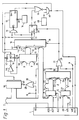
- Figure 1 shows a programmed digital data processing system which comprises a programmed microcomputer 1 provided with an external address latch 5, and a watch-dog circuit arrangement.
- Microcomputer 1 has lower order combined address and data bus lines AD0 ... AD7 and higher order address bus lines A8 ... A15 which may be coupled to other parts (not shown) of the system, for example to a program and/or data store, as indicated at 2, 3 and 4. Because the bus lines AD0 ... AD7 have a dual function the address latch 5 is provided in known manner. When microcomputer 1 outputs a 16-bit address it also outputs an address latch enable signal on an output ALE which is connected to a strobe input 7 of the latch 5. This signal causes latch 5 to store the eight lower order address bits presented to its input 6 and apply them to, inter alia, the output 4, the eight higher order address bits being applied to the output 3, after which the address/data bus lines AD0 ...
- AD7 become available for the inputting to and/or outputting from microcomputer 1 of data bits, inter alia via the data input/output 2.
- Microcomputer 1 also has in known manner an output RD for an active-low read control signal, an output WR for an active-low write control signal and an input RST for an active-low reset signal.
- Outputs RD and WR may be coupled to other parts (not shown) of the system as indicated diagrammatically at 8 and 9.
- the watch-dog arrangement comprises first and second comparators 10 and 11, an eight-into-one decoder 12, a two-into-one multiplexer 13, a frequency divide-by-two formed by a D-type flip-flop 14 the output Q of which is connected to its data input D via an inverter 44, a D-type flip-flop 15, a clock pulse source 16, a counter 17, an eight-bit-wide output buffer 18, a power-up reset pulse generator 68, two AND-gates 69 and 70, a NOR-gate 19, and two OR-gates 20 and 21.
- the output of latch 5 is connected to an eight-bit wide first input 22 of comparator 11, a fixed eight-bit byte Z being applied to an eight-bit-wide second input 23 thereof.
- the (active-low) output 27 of decoder 12 is connected to a single-bit-wide third input 24 of comparator 11 to a single-bit-wide fourth input 25 of which a fixed logic "0" signal is applied.
- Comparator 11 compares the group of bits applied to its input 22 with the group of bits applied to its input 23, and compares the bit applied to its input 24 with the bit applied to its input 25, and generates logic "O" at its output 26 if and only if correspondence occurs in both cases.
- Decoder 12 generates logic "O" at its output 27 if and only if microcomputer 1 generates a specific group of bits on the bit lines A8 ... A15 which are connected to the decoder input 46.
- the arrangement 11, 12 constitutes an address decoder for the watch-dog arrangement; comparator 11 generates logic "O" on its output 26 if and only if microcomputer 1 generates an address the eight lower-order bits of which correspond to the byte Z and the eight higher-order bits of which correspond to the bit group to which decoder 12 responds.
- the comparator input 22 and the decoder input 46 together constitute a strobe signal input of the watch-dog.
- the comparator output 26 is connected to one input of each of the OR-gates 20 and 21 to second inputs of which are connected the microcomputer outputs RD and WR respectively.
- gate 20 generates logic "O" on its output 28 if and only if microcomputer 1 addresses (strobes) the watch-dog and also generates an active-low read signal
- gate 21 generates logic "O” on its output 29 if and only if microcomputer 1 addresses (strobes) the watch-dog and also generates an active-low write signal.
- the address/data bit lines AD0 ... AD7 are also connected to an eight-bit-wide first input 30 of comparator 10 to a second eight-bit-wide input 31 of which is connected the eight-bit-wide output 32 of multiplexer 13.
- the two eight-bit-wide inputs 33 and 34 of multiplexer 13 are fed with fixed eight-bit bytes X and Y respectively.
- the control input 35 of multiplexer 13 is fed by the output of divide-by-two flip-flop 14.
- Comparator 10 has an active-low strobe signal input 36 which is connected to the output 29 of gate 21.
- the output 37 of comparator 10 is connected both to the data input D of flip-flop 15 directly and also via AND-gate 70 to the (active-low) reset input RS of counter 17.
- the (negative-edge-responsive) clock input 38 of flip-flop 15 is connected to the output of gate 21 and the clock input 39 of counter 17 is connected to the output of clock signal generator 16.
- the two inputs of gate 19 are connected to the output Q of flip-flop 15 and to the most significant bit output Qn of counter 17 respectively, its output being connected via AND-gate 69 to the active-low input RST of microcomputer 1, to the active-low asynchronous reset inputs RST of flip-flops 14 and 15, and to the second input of AND-gate 70.
- the second input of AND-gate 69 is fed from the output of the generator 68 which produces a logic "0" output pulse for a short time each time the system is powered up.
- Generator 68 may comprise, for example, a Schmitt trigger circuit the input of which is connected to one power supply line via a capacitor and to the other power supply line via a resistor.
- microcomputer 1 flip-flops 14 and 15, and counter 17 are reset on power-up and also should either the output of flip-flop 15 or the most significant bit output of counter 17 become logic "1".
- flip-flop 14 When flip-flop 14 is in the reset state it controls multiplexer 13 to supply the byte X to the input 31 of comparator 10.
- the most-significant-but-one bit output Qn-1 of counter 17 is coupled to all the bit lines AD0 ... AD7 via the multiple output buffer 18, an active-low output-enable signal input 40 of which is connected to the output 28 of gate 20.
- the output Qn-1 of counter 17 is also connected to the (negative-edge-responsive) clock input 41 of divide-by-two flip-flop 14 and also to a single-bit third input 42 of comparator 10.
- a single-bit fourth input 43 of comparator 10 is supplied with a fixed logic "1" signal.
- the signal level on the output 37 of comparator 10 is normally logic "1". Comparator 10, if and only if a logic "O" level is present on its strobe input 36, compares the byte presented to its input 30 from the bit lines AD0 ...
- AD7 with the byte (X or Y) presented to its input 31 by the multiplexer 13, and compares the level on its input 42 with the logic "1" presented to its input 43, and generates logic "O” on its output 37 if and only if correspondence occurs in both cases.
- microcomputer 1 addresses the watch-dog arrangement in two different modes, viz a read mode and a write mode in accordance with whether it produces a logic "O" on its output RD or a logic “O” on its output WR in conjunction with that address on the lines AD0 ... A15 which results in the production by comparator 11 of logic "O” on its output 26.
- the resulting enabling of the buffer 18 by the output signal of gate 20 causes this buffer to write the logic state of output Qn-1 of counter 17 onto the bus lines AD0-AD7 and hence to the microcomputer 1 which can thus ascertain what this logic state is.
- microcomputer 1 in normal operation puts that one of the bytes X and Y which is currently being presented to input 31 of comparator 10 by multiplexer 13 onto the bit lines AD0 ... AD7.
- output Qn-1 of counter 17 is in fact logic "1" comparator 10
- strobed by the logic "O” fed to its input 36 by gate 21 produces logic “O” on its output 37.
- This logic “O” resets the contents of counter 17 to zero and is also stored in flip-flop 15 which is clocked by the negative-going transition on the output of gate 21.
- the bytes X and Y are put on to the bit lines AD0 ... AD7 alternately for successive accesses of the watch-dog in the write mode, input 30 of comparator 10 therefore constituting an 8-bit wide input for a reset signal for timer/counter 17.
- a reset signal will be applied to microcomputer 1 and flip-flops 14 and 15 by gate 19 if either of the two inputs of gate 19 become logic "1" for some reason.
- a first way in which this can happen is because counter 17 (which is continuously clocked by source 16) is not reset sufficiently frequently to prevent its most significant bit output Qn from becoming logic "1".
- the program implemented by microcomputer 1 is arranged to contain watch-dog write operations at sufficiently short intervals to ensure that in normal operation this situation never occurs, provided that each such write operation gives the results set forth in the immediately preceding paragraph above.
- comparator 10 fails to produce logic "O” on its output 37 then logic "1" will be clocked into flip-flop 15, appear at its output Q and thus be applied to NOR-gate 19, resulting in a reset signal being applied immediately to microcomputer 1, i.e. without waiting for output Qn of counter 17 to become logic "1".
- microcomputer 1 in addition to the microcomputer being reset in response to the counter overflowing, in the system of Figure 1 resetting of microcomputer 1 also occurs directly in response to the generation by microcomputer 1 of a byte other than the correct one, X or Y, on the address/data bit lines AD0 ... AD7 when the watch-dog is addressed in the write mode, because flip-flop 15 is set under these conditions.
- microcomputer 1 will be reset directly should one or more of the bit outputs AD0 ... AD7 malfunction (and in fact also should one or more of the bit outputs A8 ... A15 malfunction), and also should microcomputer 1 erroneously enter a short program loop in which it does not produce the bytes X and Y alternately.
- microcomputer 1 may be programmed to store these bytes in RAM, retrieving them and rewriting the retrieved byte each time they are required. If this is the case the watch-dog arrangement will provide a check on whether the relevant part of RAM becomes corrupted for some reason, for example if the program causes the relevant storage locations to be overwritten, as may occur in certain error situations. If this should occur a reset signal for the microcomputer will be automatically generated.
- the alternating bytes X and Y may each be derived from the other; each may be, for example, the complement of the other.
- the microcomputer then being programmed to access this location each time X or Y is required, supply its contents to the watch-dog, and write the accessed byte back to the same location and, in between each pair of successive such accesses, convert the stored byte into the other while performing further program steps between each such conversion operation and the immediately preceding and immediately succeeding access/supply operations.
- the bytes X and Y are preferably 10101010 and 01010101 respectively, to provide some check on cross-talk between adjacent ones of the bit lines AD0 ... AD7.
- This feature can provide a further check on the correct implementation of the program in microcomputer 1, and is the reason for the provision of the output buffers 18 and the facility for addressing the watch-dog arrangement in the read mode.
- the microcomputer 1 can be programmed to periodically address the watch-dog in the read mode to ascertain the logic state of output Qn-1 of counter 17 and thereby determine when this state has changed from "O" to "1" and set a flag when this has occurred.
- the write mode addressing steps also included in the program may be arranged to actually take place, also resetting the flag, only if the flag is in fact set at the relevant time.
- the period of the rectangular-wave signal appearing at output Qn-1 is, of course, known, being determined by the output frequency of generator 16 and the capacity of counter 17.
- the frequency of the read-mode addressing steps and the interval between each such step and the next write-mode addressing step can therefore be chosen such as to ensure that, in normal operation, each time such a write-mode addressing step occurs, if the flag is set then the signal at output Qn-1 is still logic "1".
- each write mode addressing step is spaced in time as far as possible in the program from the immediately preceding read mode addressing step this will reduce the likelihood that, should a short program loop entered by microcomputer 1 actually include a watch-dog write-mode addressing step, it will also include the watch-dog read-mode addressing step required to prime it.
- a further advantage of testing output Qn-1 and only writing to the watch-dog when the level thereat has changed from "O" to "1" is that the repetition rate of the watch-dog write operations is automatically adjusted to lie between one half and one times the frequency of the signal at output Qn-1, enabling this repetition rate to be optimised and to be little dependent on what branches the program actually takes each time it is carried out.
- FIG. 2 An example of the parts of the program with which microcomputer 1 may be programmed which are relevant to the present invention is shown in Figure 2, which takes the form a of flow chart.
- Figure 2 takes the form a of flow chart.
- the various blocks have the following significances.
- step 50 the byte X is written in step 51 to a location AD in RAM which is preferably one which is likely to be overwritten should the program malfunction. Moreover a flag F1 which is used to indicate when the signal at output Qn-1 of counter 17 has been determined as being logic "1” is set to logic "O” as is a flag F2 which is used to indicate when the watch-dog has been written to. Then (step 52) part of the main program of the microcomputer is carried out. It is then tested in step 53 whether output Qn-1 is logic "1", microcomputer 1 first generating address byte Z on its outputs AD0 ... AD7 and the byte to which decoder 12 responds on its outputs A8 ...
- step 54 If Qn-1 is "1" (Y) flag F1 is set to "1" in step 54, and in any case another part of the main program is then carried out in block 55. After this it is ascertained in step 56 whether flag F1 is set, i.e. whether it was determined in step 53 that Qn-1 was logic "1". If it was (Y), the contents of RAM address AD (initially byte X, for example 01010101), are written to the watch-dog in step 57 (and also rewritten to the address AD) microcomputer 1 first generating address byte Z on its outputs AD0 ...
- step 57 when step 57 occurs, output Qn-1 will still be logic "1", resulting in counter 17 being reset, changing over flip-flop 14, but no general reset occurring.
- Flag F1 is then reset and flag F2 is set to "1" (block 58) indicating that the watch-dog has been written to.
- the program then proceeds to block 59, as it does directly from step 56 if it is found there that flag F1 is not set (N).
- Block 59 represents the next part of the main program, after which flag F2 is tested (step 60) to ascertain if step 57 in fact took place. If it did (Y) the byte in RAM address AD is complemented and rewritten in step 61 so that it becomes Y to conform with the new state of multiplexer 13, after which flag F2 is reset in step 62 and the program proceeds back to block 52, as it does directly if the result of test 60 is "no" (N).
- step 57 In order that, if the result of test 53 is "yes", output Qn-1 of counter 17 will still be “1" when step 57 is performed it is arranged that, provided the system is operating correctly, the time interval between successive pairs of tests 53 plus the time to the next step 57 if it is in fact carried out is always less than one half the period of the signal appearing at output Qn-1 of counter 17.
- a delay element may be provided at the output of gate 69 in Figure 1 to ensure that any reset signal produced thereat has a sufficiently long duration before the counter 17 or flip-flop 15 which may have given rise to it is itself reset.
Landscapes
- Engineering & Computer Science (AREA)
- Theoretical Computer Science (AREA)
- Quality & Reliability (AREA)
- Physics & Mathematics (AREA)
- General Engineering & Computer Science (AREA)
- General Physics & Mathematics (AREA)
- Debugging And Monitoring (AREA)
Description
- This invention relates to a programmed digital data processing system including a watch-dog circuit arrangement, which arrangement comprises timer means to which is coupled a reset signal input, for generating an output signal in response to an interval between successive resets of the timer means exceeding a predetermined length, said system being programmed to execute a main program and to supply predetermined reset signals to said reset signal input, and thereby reset the timer means, at intervals which do not exceed said predetermined length and being arranged to respond to the generation of a said output signal by assuming a predetermined state, said reset signals each being in the form of a multibit word having a predetermined value, which predetermined value changes for successive reset signals in a predetermined manner, said arrangement being arranged to also generate a said output signal should each multibit reset signal supplied to the reset signal input not have the relevant predetermined value.
- Watch-dog circuit arrangements are well-known, and serve to monitor the correct implementation of a data processing system program. The timer means may, for example, take the form of a continuously clocked counter which produces an overflow signal (the timer means output signal) should its capacity be exceeded, the counter being provided with a reset input a signal applied to which results in the counter contents being set to zero. In its simplest form the data processing system could comprise a suitably programmed microcomputer a single bit-line of one of the output ports of which is coupled to the reset input of the counter, the computer being programmed in such a way that a signal which resets the counter is periodically applied to the signal bit-line at such a rate that the counter is always reset before its contents overflow. Thus in normal operation the counter never produces an overflow signal. If, however, the implementation of the program should cease for some reason, resulting in the resetting of the counter also ceasing, then the counter contents will eventually reach the maximum, and the counter will produce an overflow signal. The overflow signal output may, for example, be coupled to a general reset input of the microcomputer, so that the microcomputer is itself reset under these circumstances. A similar result is obtained if the microcomputer should incorrectly enter a program loop which does not include a step entailing the application of a reset signal for the timer to the single bit line, or which does include such a step but in which this step is repeated insufficiently frequently to prevent the counter contents overflowing.
- GB-A-1 522 810 discloses a system as defined in the first paragraph, i.e. a system which constitutes an elaboration of the simple system discussed so far. In this more elaborate system each reset signal takes the form of a multibit word having one of a pair of predetermined values which alternate and are each the complement of the other. The timer means is only reset in response to the supply of such a reset signal if that signal has the relevant predetermined value. In consequence, if for example a data bus which may be used to communicate the reset signals to the watch-dog circuit arrangement becomes faulty, thereby mutilating the reset signals, the timer means will not in fact be reset and the output signal will in consequence be generated. (In the known system the output signal is used to activate an alarm). Thus a check is also made on the correct operation of the data bus. One of the two multibit words is stored, apparently permanently, in memory. When a reset operation for the timer means is performed this word is written into a register and thence sent as a reset signal to the watch-dog arrangement. The contents of the register are then complemented and the result is also sent to the watch-dog arrangement, the two words thus sent together resulting in resetting of the timer means. The above four steps are immediately successive steps in the system program and, because of this, it is very likely that if the computer should erroneously enter a program loop in which watch-dog reset signals are still produced at substantially the normal rate, the words will still occur in the correct sequence, with the result that the timer means will still be reset each time, contrary to what is required.
- It is an object of the invention to mitigate this disadvantage, and to this end a programmed digital data processing system is, according to the invention, characterised in that the system is programmed to assign, during each interval between the supply of successive said reset signals to said reset signal input, the next predetermined value to a said multibit word for transmission as the next reset signal, and to perform further main program steps between each such assigning operation and the immediately preceding and immediately succeeding supply of a reset signal.
- It has now been recognised that by effectively providing a predetermined value assigning step between the supply of each reset word to the reset signal input and the supply of the next such reset word to the reset signal input, and including further program steps between each such assigning step and the immediately preceding and immediately succeeding reset signal supply steps, a program structure is obtained which, if the system program enters an erroneous loop, is very likely to result in the assigning and reset signal supplying steps occurring in an incorrect order, or in one or the other not occurring at all, with the result that, even if reset signals are still supplied at substantially the normal rate, it is very likely that the watch-dog circuit arrangement will generate its output signal, as required.
- The predetermined manner in which the predetermined value changes for successive reset signals may in principle be any manner whatsoever (bearing in mind that it is necessary for the watch-dog arrangement to "know" the resulting sequence of multibit words which will be applied to its reset signal input in operation.) Thus, each predetermined value may be derived from the preceding one by, for example, an arithmetic operation, e.g. by addition or subtraction of a constant. Preferably, however, the predetermined value changes for successive reset signals in accordance with a cyclic sequence, enabling, for example, each predetermined value to be stored permanently in the watch-dog arrangement for comparison with the relevant reset signal received. In principle such a cyclic sequence can contain any number of said predetermined values, and each predetermined value need not in principle have any particular relationship to any of the other predetermined values. Preferably, however, the cyclic sequence consists of only two predetermined values each of which is a complemented version of the other, for example a byte consisting of alternate "0"s and "1"s enabling a check to be made on cross-talk between adjoining bits. Either one or both of these may be stored, preferably in random access memory, at any given time, from which it may be read for the relevant reset signal in an effectively non-destructive manner. If only one is stored at any given time, each said assigning operation may comprise complementing the currently stored value and replacing this currently stored value by the result. If both are stored at any given time, each said assigning operation may comprise changing over a pointer from one stored value to the other. Storing one or both values in random access memory provides a check on the relevant part of RAM being incorrectly overwritten in response to erroneous operation of the program.
- It may be arranged that the timer means simply responds to each said reset signal only if the reset signal has the predetermined value, so that the timer means itself generates a said output signal when reset signals having the predetermined value are not supplied to the reset signal input during an interval which exceeds the predetermined length, even though reset signals having other values may be supplied during that interval. Preferably, however, the arrangement is arranged to respond directly to the supply of a reset signal not having the predetermined value to the reset signal input by generating a said output signal.
- The system may be programmed to supply each reset signal to reset signal input within a respective predetermined time window and the watch-dog circuit arrangement may be arranged to also generate a said output signal should each reset signal supplied to the reset signal input not be supplied thereto within a said predetermined time window. It may be arranged, for example, that the watch-dog arrangement simply treats the supply of a reset signal to the reset signal input as constituting a boundary of a said interval only if this supply occurs within such a predetermined time window, so that the timer means itself generates a said output signal when reset signals are not supplied to the reset signal input within respective said time windows during an interval which exceeds the predetermined length, even though reset signals may still be supplied outside such time windows. Preferably, however, the arrangement is arranged to respond directly to the supply of a reset signal to the reset signal input outside a said time window by generating a said output signal. During a malfunction it can be that reset signals are supplied outside such time windows, in which case the malfunction will be responded to. It may be arranged that each said predetermined time window has a predetermined relationship to the instant at which the immediately preceding reset signal was applied to the reset signal input. Thus, if for example the timer means comprises a continuously clocked binary counter to a reset input of which the reset signal input is coupled each time window may correspond to the time during which a particular bit of the counter contents has a given value. If this is the case the system may be programmed to periodically test the value of said particular bit to determine when it has changed to the given value, to supply a reset signal to the reset signal input after such a change has been detected, and to perform further program steps between the detection of such a change and the subsequent supply of the reset signal. Performing the further program steps, i.e. separating the reset signal in time from the detection which has given rise to it, makes it less likely that, during a malfunction, the reset signal will be supplied within a said time window.
- Preferably the system is programmed to strobe the watch-dog circuit arrangement, for example by generating an address specific to the watch-dog arrangement, each time a reset signal is supplied to the reset signal input. This can facilitate, for example, a direct response of the watch-dog arrangement to the supply of a reset signal not having the predetermined value and/or a reset signal outside a said time window to the reset signal input.
- If the system comprises a programmed microcomputer provided with an external address latch the address latch and the watch-dog circuit arrangement are preferably integrated on the same semiconductor chip.
- An embodiment of the invention will now be described, by way of example, with reference to the accompanying diagramatic drawings in which,
- Figure 1 is a block diagram of the embodiment, and
- Figure 2 is a flow chart illustrating the operation of the embodiment of Figure 1.
- Figure 1 shows a programmed digital data processing system which comprises a programmed microcomputer 1 provided with an
external address latch 5, and a watch-dog circuit arrangement. - Microcomputer 1 has lower order combined address and data bus lines AD0 ... AD7 and higher order address bus lines A8 ... A15 which may be coupled to other parts (not shown) of the system, for example to a program and/or data store, as indicated at 2, 3 and 4. Because the bus lines AD0 ... AD7 have a dual function the
address latch 5 is provided in known manner. When microcomputer 1 outputs a 16-bit address it also outputs an address latch enable signal on an output ALE which is connected to a strobe input 7 of thelatch 5. This signal causeslatch 5 to store the eight lower order address bits presented to itsinput 6 and apply them to, inter alia, the output 4, the eight higher order address bits being applied to theoutput 3, after which the address/data bus lines AD0 ... AD7 become available for the inputting to and/or outputting from microcomputer 1 of data bits, inter alia via the data input/output 2. Microcomputer 1 also has in known manner an output RD for an active-low read control signal, an output WR for an active-low write control signal and an input RST for an active-low reset signal. Outputs RD and WR may be coupled to other parts (not shown) of the system as indicated diagrammatically at 8 and 9. - The watch-dog arrangement comprises first and
second comparators decoder 12, a two-into-onemultiplexer 13, a frequency divide-by-two formed by a D-type flip-flop 14 the output Q of which is connected to its data input D via aninverter 44, a D-type flip-flop 15, aclock pulse source 16, acounter 17, an eight-bit-wide output buffer 18, a power-upreset pulse generator 68, two AND-gates gates latch 5 is connected to an eight-bit widefirst input 22 ofcomparator 11, a fixed eight-bit byte Z being applied to an eight-bit-widesecond input 23 thereof. The (active-low)output 27 ofdecoder 12 is connected to a single-bit-wide third input 24 ofcomparator 11 to a single-bit-widefourth input 25 of which a fixed logic "0" signal is applied.Comparator 11 compares the group of bits applied to itsinput 22 with the group of bits applied to itsinput 23, and compares the bit applied to its input 24 with the bit applied to itsinput 25, and generates logic "O" at itsoutput 26 if and only if correspondence occurs in both cases.Decoder 12 generates logic "O" at itsoutput 27 if and only if microcomputer 1 generates a specific group of bits on the bit lines A8 ... A15 which are connected to thedecoder input 46. Thus thearrangement comparator 11 generates logic "O" on itsoutput 26 if and only if microcomputer 1 generates an address the eight lower-order bits of which correspond to the byte Z and the eight higher-order bits of which correspond to the bit group to whichdecoder 12 responds. Thus thecomparator input 22 and thedecoder input 46 together constitute a strobe signal input of the watch-dog. Thecomparator output 26 is connected to one input of each of the OR-gates gate 20 generates logic "O" on itsoutput 28 if and only if microcomputer 1 addresses (strobes) the watch-dog and also generates an active-low read signal, andgate 21 generates logic "O" on itsoutput 29 if and only if microcomputer 1 addresses (strobes) the watch-dog and also generates an active-low write signal. - The address/data bit lines AD0 ... AD7 are also connected to an eight-bit-wide
first input 30 ofcomparator 10 to a second eight-bit-wide input 31 of which is connected the eight-bit-wide output 32 ofmultiplexer 13. The two eight-bit-wide inputs multiplexer 13 are fed with fixed eight-bit bytes X and Y respectively. Thecontrol input 35 ofmultiplexer 13 is fed by the output of divide-by-two flip-flop 14.Comparator 10 has an active-lowstrobe signal input 36 which is connected to theoutput 29 ofgate 21. Theoutput 37 ofcomparator 10 is connected both to the data input D of flip-flop 15 directly and also via AND-gate 70 to the (active-low) reset input RS ofcounter 17. The (negative-edge-responsive)clock input 38 of flip-flop 15 is connected to the output ofgate 21 and the clock input 39 ofcounter 17 is connected to the output ofclock signal generator 16. The two inputs ofgate 19 are connected to the output Q of flip-flop 15 and to the most significant bit output Qn ofcounter 17 respectively, its output being connected viaAND-gate 69 to the active-low input RST of microcomputer 1, to the active-low asynchronous reset inputs RST of flip-flops AND-gate 70. The second input ofAND-gate 69 is fed from the output of thegenerator 68 which produces a logic "0" output pulse for a short time each time the system is powered up.Generator 68 may comprise, for example, a Schmitt trigger circuit the input of which is connected to one power supply line via a capacitor and to the other power supply line via a resistor. Thus microcomputer 1, flip-flops flop 15 or the most significant bit output ofcounter 17 become logic "1". When flip-flop 14 is in the reset state it controlsmultiplexer 13 to supply the byte X to theinput 31 ofcomparator 10. - The most-significant-but-one bit output Qn-1 of
counter 17 is coupled to all the bit lines AD0 ... AD7 via themultiple output buffer 18, an active-low output-enablesignal input 40 of which is connected to theoutput 28 ofgate 20. The output Qn-1 ofcounter 17 is also connected to the (negative-edge-responsive)clock input 41 of divide-by-two flip-flop 14 and also to a single-bitthird input 42 ofcomparator 10. A single-bitfourth input 43 ofcomparator 10 is supplied with a fixed logic "1" signal. The signal level on theoutput 37 ofcomparator 10 is normally logic "1".Comparator 10, if and only if a logic "O" level is present on itsstrobe input 36, compares the byte presented to itsinput 30 from the bit lines AD0 ... AD7 with the byte (X or Y) presented to itsinput 31 by themultiplexer 13, and compares the level on itsinput 42 with the logic "1" presented to itsinput 43, and generates logic "O" on itsoutput 37 if and only if correspondence occurs in both cases. - In operation microcomputer 1 addresses the watch-dog arrangement in two different modes, viz a read mode and a write mode in accordance with whether it produces a logic "O" on its output RD or a logic "O" on its output WR in conjunction with that address on the lines AD0 ... A15 which results in the production by
comparator 11 of logic "O" on itsoutput 26. In the read mode the resulting enabling of thebuffer 18 by the output signal ofgate 20 causes this buffer to write the logic state of output Qn-1 ofcounter 17 onto the bus lines AD0-AD7 and hence to the microcomputer 1 which can thus ascertain what this logic state is. In the write mode (which in normal operation only occurs when the said logic state is "1"; see below) microcomputer 1 in normal operation puts that one of the bytes X and Y which is currently being presented to input 31 ofcomparator 10 bymultiplexer 13 onto the bit lines AD0 ... AD7. Assuming that output Qn-1 ofcounter 17 is in fact logic "1"comparator 10, strobed by the logic "O" fed to itsinput 36 bygate 21, produces logic "O" on itsoutput 37. This logic "O" resets the contents ofcounter 17 to zero and is also stored in flip-flop 15 which is clocked by the negative-going transition on the output ofgate 21. Both inputs ofgate 19 are therefore logic "O", so that reset inputs RST of microcomputer 1 and flip-flops counter 17 results in the level at its output Qn-1 changing from logic "1" to logic "O", and this transition changes over the frequency divider-by-two flip-flop 14 to its other output state, thereby causingmultiplexer 13 to feed the other of the bytes X and Y to input 31 ofcomparator 10. In normal operation the next time microcomputer 1 accesses the watch-dog in the write mode it is arranged to put this other byte onto the bit lines AD0 ... AD7, so a similar result occurs to that just described. The bytes X and Y are put on to the bit lines AD0 ... AD7 alternately for successive accesses of the watch-dog in the write mode,input 30 ofcomparator 10 therefore constituting an 8-bit wide input for a reset signal for timer/counter 17. - A reset signal will be applied to microcomputer 1 and flip-
flops gate 19 if either of the two inputs ofgate 19 become logic "1" for some reason. A first way in which this can happen is because counter 17 (which is continuously clocked by source 16) is not reset sufficiently frequently to prevent its most significant bit output Qn from becoming logic "1". The program implemented by microcomputer 1 is arranged to contain watch-dog write operations at sufficiently short intervals to ensure that in normal operation this situation never occurs, provided that each such write operation gives the results set forth in the immediately preceding paragraph above. However, if the program implementation should stop for some reason, or should erroneously enter a program loop which does not include a watch-dog write operation, then it will be evident that output Qn ofcounter 17 will eventually become logic "1", resetting microcomputer 1 viagate 19 as required. This of course would also be the case with the known watch-dog arrangements. However, the arrangement shown also responds to certain other malfunctions of the system, as will be explained below. A second way in which one of the two inputs ofgate 19 will become logic "1", resetting microcomputer 1, is by the setting of flip-flop 15. Flip-flop 15 is clocked each time the watch-dog is addressed in the write mode, and if the correct byte X or Y should not then be present on the bit lines AD0 ... AD7, so thatcomparator 10 fails to produce logic "O" on itsoutput 37 then logic "1" will be clocked into flip-flop 15, appear at its output Q and thus be applied to NOR-gate 19, resulting in a reset signal being applied immediately to microcomputer 1, i.e. without waiting for output Qn ofcounter 17 to become logic "1". - As a first point it should be noted that, in addition to the microcomputer being reset in response to the counter overflowing, in the system of Figure 1 resetting of microcomputer 1 also occurs directly in response to the generation by microcomputer 1 of a byte other than the correct one, X or Y, on the address/data bit lines AD0 ... AD7 when the watch-dog is addressed in the write mode, because flip-
flop 15 is set under these conditions. Thus microcomputer 1 will be reset directly should one or more of the bit outputs AD0 ... AD7 malfunction (and in fact also should one or more of the bit outputs A8 ... A15 malfunction), and also should microcomputer 1 erroneously enter a short program loop in which it does not produce the bytes X and Y alternately. Furthermore, microcomputer 1 may be programmed to store these bytes in RAM, retrieving them and rewriting the retrieved byte each time they are required. If this is the case the watch-dog arrangement will provide a check on whether the relevant part of RAM becomes corrupted for some reason, for example if the program causes the relevant storage locations to be overwritten, as may occur in certain error situations. If this should occur a reset signal for the microcomputer will be automatically generated. The alternating bytes X and Y may each be derived from the other; each may be, for example, the complement of the other. If this is the case only a single RAM location will be required to store them, the microcomputer then being programmed to access this location each time X or Y is required, supply its contents to the watch-dog, and write the accessed byte back to the same location and, in between each pair of successive such accesses, convert the stored byte into the other while performing further program steps between each such conversion operation and the immediately preceding and immediately succeeding access/supply operations. If this is the case the bytes X and Y are preferably 10101010 and 01010101 respectively, to provide some check on cross-talk between adjacent ones of the bit lines AD0 ... AD7. - As a second point, attention is drawn to the connection of the most signficant bit but one output Qn-1 of
counter 17 to input 42 of comparator 10 (in which the level on this output is compared with the logic "1" applied to input 43). This means that when the watch-dog is addressed in the write mode then, unless output Qn-1 is then logic "1",comparator 10 will not produce a logic "O" output signal even if microcomputer 1 then applies the correct byte X or Y to the bit-lines ADO ... AD7. In other words, if the watch-dog is addressed in the write mode at a time when output Qn-1 ofcounter 17 is logic "O", flip-flop 15 will apply a reset signal to microcomputer 1 viagate 19. This feature can provide a further check on the correct implementation of the program in microcomputer 1, and is the reason for the provision of the output buffers 18 and the facility for addressing the watch-dog arrangement in the read mode. The microcomputer 1 can be programmed to periodically address the watch-dog in the read mode to ascertain the logic state of output Qn-1 ofcounter 17 and thereby determine when this state has changed from "O" to "1" and set a flag when this has occurred. The write mode addressing steps also included in the program may be arranged to actually take place, also resetting the flag, only if the flag is in fact set at the relevant time. The period of the rectangular-wave signal appearing at output Qn-1 is, of course, known, being determined by the output frequency ofgenerator 16 and the capacity ofcounter 17. The frequency of the read-mode addressing steps and the interval between each such step and the next write-mode addressing step can therefore be chosen such as to ensure that, in normal operation, each time such a write-mode addressing step occurs, if the flag is set then the signal at output Qn-1 is still logic "1". The condition for this is that the interval between each pair of successive read-mode addressing steps plus the interval between the second of these steps and the next write mode addressing step must be less than half the period which the signal at output Qn-1 would have were counter 17 allowed to run freely.) If, within this constraint, each write mode addressing step is spaced in time as far as possible in the program from the immediately preceding read mode addressing step this will reduce the likelihood that, should a short program loop entered by microcomputer 1 actually include a watch-dog write-mode addressing step, it will also include the watch-dog read-mode addressing step required to prime it. A further advantage of testing output Qn-1 and only writing to the watch-dog when the level thereat has changed from "O" to "1" is that the repetition rate of the watch-dog write operations is automatically adjusted to lie between one half and one times the frequency of the signal at output Qn-1, enabling this repetition rate to be optimised and to be little dependent on what branches the program actually takes each time it is carried out. - An example of the parts of the program with which microcomputer 1 may be programmed which are relevant to the present invention is shown in Figure 2, which takes the form a of flow chart. In this Figure the various blocks have the following significances.
- 50 -
- Start. (A reset signal applied to reset input RST of microcomputer 1 in Figure 1 results in a return of the program to this stage).
- 51 -
- Initialise, including the writing of byte X (see the description of Figure 1) to a specific address AD in RAM and the setting of flags F1 and F2 to logic "O".
- 52 -
- Part of main program.
- 53 -
- Is output Qn-1 of
counter 17 in Figure 1 logic "1"? - 54 -
- Set flag F1 to logic "1".
- 55 -
- Part of main program
- 56 -
- Is flag F1 logic "1"?
- 57 -
- Write contents of RAM address AD to watch-dog.
- 58 -
- Set flag F2 to logic "1". Set flag F1 to logic "0".
- 59 -
- Part of main program.
- 60 -
- Is flag F2 logic "1"?
- 61 -
- Complement contents of RAM address AD.
- 62 -
- Set flag F2 to logic "O".
- After START (stage 50) the byte X is written in
step 51 to a location AD in RAM which is preferably one which is likely to be overwritten should the program malfunction. Moreover a flag F1 which is used to indicate when the signal at output Qn-1 ofcounter 17 has been determined as being logic "1" is set to logic "O" as is a flag F2 which is used to indicate when the watch-dog has been written to. Then (step 52) part of the main program of the microcomputer is carried out. It is then tested instep 53 whether output Qn-1 is logic "1", microcomputer 1 first generating address byte Z on its outputs AD0 ... AD7 and the byte to whichdecoder 12 responds on its outputs A8 ... A15, and then logic "O" on its output RD (read mode), reading the output signal of the thus enabledbuffer 18 on its outputs/inputs AD0 ... AD7. If Qn-1 is "1" (Y) flag F1 is set to "1" instep 54, and in any case another part of the main program is then carried out inblock 55. After this it is ascertained instep 56 whether flag F1 is set, i.e. whether it was determined instep 53 that Qn-1 was logic "1". If it was (Y), the contents of RAM address AD (initially byte X, for example 01010101), are written to the watch-dog in step 57 (and also rewritten to the address AD) microcomputer 1 first generating address byte Z on its outputs AD0 ... AD7 and the byte to whichdecoder 12 responds on its outputs A8 ... A15, and then logic "O" on its output WR (write mode) and the byte X from RAM address AD on its outputs AD0 ... AD7. In normal operation, whenstep 57 occurs, output Qn-1 will still be logic "1", resulting incounter 17 being reset, changing over flip-flop 14, but no general reset occurring. Flag F1 is then reset and flag F2 is set to "1" (block 58) indicating that the watch-dog has been written to. The program then proceeds to block 59, as it does directly fromstep 56 if it is found there that flag F1 is not set (N).Block 59 represents the next part of the main program, after which flag F2 is tested (step 60) to ascertain ifstep 57 in fact took place. If it did (Y) the byte in RAM address AD is complemented and rewritten instep 61 so that it becomes Y to conform with the new state ofmultiplexer 13, after which flag F2 is reset instep 62 and the program proceeds back to block 52, as it does directly if the result oftest 60 is "no" (N). - In order that, if the result of
test 53 is "yes", output Qn-1 ofcounter 17 will still be "1" whenstep 57 is performed it is arranged that, provided the system is operating correctly, the time interval between successive pairs oftests 53 plus the time to thenext step 57 if it is in fact carried out is always less than one half the period of the signal appearing at output Qn-1 ofcounter 17. - If required, a delay element (not shown) may be provided at the output of
gate 69 in Figure 1 to ensure that any reset signal produced thereat has a sufficiently long duration before thecounter 17 or flip-flop 15 which may have given rise to it is itself reset. - It will be appreciated that the parts of the system shown in Figure 1, other than the microcomputer 1, may be very conveniently all be integrated on the same semiconductor chip.
- From reading the present disclosure, other modifications will be apparent to persons skilled in the art. Such modifications may involve other features which are already known in the design, manufacture and use of systems and devices and component parts thereof and which may be used instead of or in addition to features already described herein.
Claims (9)
- A programmed digital data processing system including a watch-dog circuit arrangement, which arrangement comprises timer means to which is coupled a reset signal input, for generating an output signal in response to an interval between successive resets of the timer means exceeding a predetermined length, said system being programmed to execute a main program and to supply predetermined reset signals to said reset signal input, and thereby reset the timer means, at intervals which do not exceed said predetermined length and being arranged to respond to the generation of a said output signal by assuming a predetermined state, said reset signals each being in the form of a multibit word having a predetermined value, which predetermined value changes for successive reset signals in a predetermined manner, said arrangement being arranged to also generate a said output signal should each multibit reset signal supplied to the reset signal input not have the relevant predetermined value, characterised in that the system is programmed to assign, during each interval between the supply of successive said reset signals to said reset signal input, the next predetermined value to a said multibit word for transmission as the next reset signal, and to perform further main program steps between each such assigning operation and the immediately preceding and immediately succeeding supply of a reset signal.
- A system as claimed in Claim 1 wherein said predetermined value changes for successive reset signals in accordance with a cyclic sequence.
- A system as claimed in Claim 2, wherein the sequence consists of two predetermined values each of which is a complemented version of the other.
- A system as claimed in Claim 3, wherein each multibit word is a byte consisting of alternate "0"s and "1"s.
- A system as claimed in any preceding claim, wherein the multibit word is stored in random access memory from which it is read for each said reset signal in an effectively non-destructive manner.
- A system as claimed in any preceding claim, wherein each assigning operation comprises calculating the predetermined value of the multibit word for transmission as the next reset signal from the multibit word transmitted as the immediately preceding reset signal.
- A system as claimed in any preceding claim, wherein the watch-dog circuit arrangement is arranged to respond directly to the supply of a reset signal not having the relevant predetermined value to the reset signal input by generating a said output signal.
- A system as claimed in any preceding claim, programmed to strobe the watch-dog circuit arrangement each time a reset signal is supplied to the reset signal input.
- A system as claimed in any preceding claim, comprising a programmed microcomputer provided with an external address latch, wherein the address latch and the watch-dog circuit arrangement are integrated on the same semiconductor chip.
Applications Claiming Priority (2)
| Application Number | Priority Date | Filing Date | Title |
|---|---|---|---|
| GB8626197 | 1986-11-03 | ||
| GB08626197A GB2197507A (en) | 1986-11-03 | 1986-11-03 | Data processing system |
Publications (3)
| Publication Number | Publication Date |
|---|---|
| EP0266836A2 EP0266836A2 (en) | 1988-05-11 |
| EP0266836A3 EP0266836A3 (en) | 1990-05-16 |
| EP0266836B1 true EP0266836B1 (en) | 1995-01-04 |
Family
ID=10606705
Family Applications (1)
| Application Number | Title | Priority Date | Filing Date |
|---|---|---|---|
| EP87202088A Expired - Lifetime EP0266836B1 (en) | 1986-11-03 | 1987-10-30 | Data processing system including a watch-dog circuit |
Country Status (7)
| Country | Link |
|---|---|
| US (1) | US5073853A (en) |
| EP (1) | EP0266836B1 (en) |
| JP (1) | JP2755581B2 (en) |
| AU (1) | AU604776B2 (en) |
| DE (1) | DE3750948T2 (en) |
| GB (1) | GB2197507A (en) |
| NZ (1) | NZ222361A (en) |
Families Citing this family (31)
| Publication number | Priority date | Publication date | Assignee | Title |
|---|---|---|---|---|
| FR2658303B1 (en) * | 1990-02-09 | 1992-06-19 | Neiman Sa | DEVICE FOR MONITORING THE OPERATION OF A MICROPROCESSOR SYSTEM OR THE LIKE. |
| GB2241799B (en) * | 1990-03-08 | 1993-12-08 | Sony Corp | Supervision of microprocessors |
| US5278976A (en) * | 1990-04-16 | 1994-01-11 | Rolm Company | Method for detecting infinite loops by setting a flag indicating execution of an idle task having lower priority than executing application tasks |
| DE4039355C2 (en) * | 1990-12-10 | 1998-07-30 | Bosch Gmbh Robert | Device for checking the function of a watchdog circuit |
| JP2758742B2 (en) * | 1991-07-19 | 1998-05-28 | 日本電気株式会社 | Malfunction detection method |
| FR2692379B1 (en) * | 1991-10-04 | 1996-08-14 | Aerospatiale Ste Nat Indle | FAULT DETECTION AND PASSIVATION PROCESS IN A DATA PROCESSING SYSTEM, AND DATA PROCESSING SYSTEM ADAPTED TO ITS IMPLEMENTATION |
| US5341497A (en) * | 1991-10-16 | 1994-08-23 | Ohmeda Inc. | Method and apparatus for a computer system to detect program faults and permit recovery from such faults |
| JP2658697B2 (en) * | 1991-12-11 | 1997-09-30 | 富士通株式会社 | Watch dock timer circuit |
| JPH0683652A (en) * | 1992-08-31 | 1994-03-25 | Sharp Corp | Micro computer system |
| JPH06168163A (en) * | 1992-09-30 | 1994-06-14 | Nec Home Electron Ltd | Method and device for monitoring cpu |
| JP3135772B2 (en) * | 1993-12-27 | 2001-02-19 | アスコ株式会社 | Vehicle safety device |
| US5948606A (en) * | 1994-03-31 | 1999-09-07 | Eastman Kodak Company | Protective top layer and photographic products containing this top layer |
| KR100311366B1 (en) * | 1994-11-28 | 2002-02-19 | 구자홍 | Controller having watch dog timer function |
| US5541943A (en) * | 1994-12-02 | 1996-07-30 | At&T Corp. | Watchdog timer lock-up prevention circuit |
| US5528756A (en) * | 1995-01-30 | 1996-06-18 | Elsag International N.V. | Method and apparatus for performing supervisory functions in digital systems and obtaining diagnostics thereof |
| US5673389A (en) * | 1995-08-31 | 1997-09-30 | Ford Motor Company | Methods and apparatus for resetting a monitored system using a gray code with alternating check bits |
| US5745386A (en) * | 1995-09-25 | 1998-04-28 | International Business Machines Corporation | Timing diagram method for inputting logic design parameters to build a testcase for the logic diagram |
| KR100252250B1 (en) * | 1996-06-28 | 2000-04-15 | 윤종용 | System recovery device |
| DE19627362C2 (en) * | 1996-07-06 | 1998-11-26 | Bosch Gmbh Robert | Circuit for initializing and monitoring a microprocessor |
| WO1998007089A1 (en) * | 1996-08-12 | 1998-02-19 | Papst-Motoren Gmbh & Co. Kg | Process and device for monitoring a microprocessor |
| DE19827430C2 (en) * | 1997-07-22 | 2001-07-12 | Siemens Ag | Monitoring procedure for the detection of infinite loops and blocked processes in a computer system |
| FR2771564B1 (en) * | 1997-11-21 | 2000-02-11 | Sextant Avionique | DEVICE FOR INITIALIZING THE POWER ON OF A DIGITAL INTEGRATED CIRCUIT |
| US6141774A (en) * | 1998-04-17 | 2000-10-31 | Infineon Technologies North America Corp. | Peripheral device with access control |
| GB9911890D0 (en) | 1999-05-22 | 1999-07-21 | Lucas Ind Plc | Method and apparatus for detecting a fault condition in a computer processor |
| US6476996B1 (en) | 2000-02-15 | 2002-11-05 | Western Digital Technologies, Inc. | Disk drive comprising an actuator driver circuit for retracting a head independent of a servo microprocessor when a spindle speed fault mode is detected |
| US6779066B2 (en) * | 2000-05-01 | 2004-08-17 | Matsushita Electric Industrial Co., Ltd. | Module having application-specific program stored therein |
| KR100820789B1 (en) * | 2001-04-06 | 2008-04-10 | 엘지전자 주식회사 | Real-time based system and its monitoring method |
| US20060235655A1 (en) * | 2005-04-18 | 2006-10-19 | Qing Richard X | Method for monitoring function execution |
| US8330502B2 (en) * | 2009-11-25 | 2012-12-11 | Freescale Semiconductor, Inc. | Systems and methods for detecting interference in an integrated circuit |
| US9697065B1 (en) | 2016-03-09 | 2017-07-04 | Nxp Usa, Inc. | Systems and methods for managing reset |
| US10157087B1 (en) | 2017-07-14 | 2018-12-18 | Nxp Usa, Inc. | Robust boot block design and architecture |
Citations (1)
| Publication number | Priority date | Publication date | Assignee | Title |
|---|---|---|---|---|
| DE2821882A1 (en) * | 1978-05-19 | 1979-11-22 | Philips Patentverwaltung | Programmed controller for electromechanical systems - uses instruction monitoring test data store receiving individual instruction series information |
Family Cites Families (26)
| Publication number | Priority date | Publication date | Assignee | Title |
|---|---|---|---|---|
| US3919533A (en) * | 1974-11-08 | 1975-11-11 | Westinghouse Electric Corp | Electrical fault indicator |
| DE2946081C3 (en) * | 1979-11-15 | 1995-09-21 | Wabco Vermoegensverwaltung | Circuit arrangement for monitoring the function of a microprocessor |
| GB2070302B (en) * | 1980-02-19 | 1985-02-13 | Omron Tateisi Electronics Co | Data communication system |
| CA1160753A (en) * | 1980-08-20 | 1984-01-17 | Canadian General Electric Company Limited | Microprocessor watchdog system |
| US4570217A (en) * | 1982-03-29 | 1986-02-11 | Allen Bruce S | Man machine interface |
| US4538273A (en) * | 1982-11-12 | 1985-08-27 | Honeywell Inc. | Dual input watchdog timer |
| JPS603045A (en) * | 1983-06-20 | 1985-01-09 | Nec Corp | Detector for program address malfunction |
| US4594685A (en) * | 1983-06-24 | 1986-06-10 | General Signal Corporation | Watchdog timer |
| JPS6039255A (en) * | 1983-08-12 | 1985-03-01 | Mitsubishi Electric Corp | Reset circuit of watchdog timer |
| DE3343227A1 (en) * | 1983-11-30 | 1985-06-05 | Robert Bosch Gmbh, 7000 Stuttgart | METHOD FOR MONITORING ELECTRONIC COMPUTERS, IN PARTICULAR MICROPROCESSORS |
| US4759952A (en) * | 1984-01-26 | 1988-07-26 | Learonal, Inc. | Process for printed circuit board manufacture |
| JPS60193060A (en) * | 1984-03-14 | 1985-10-01 | Mitsubishi Electric Corp | Watchdog timer circuit |
| JPS60263235A (en) * | 1984-06-12 | 1985-12-26 | Omron Tateisi Electronics Co | Microcomputer system |
| US4649537A (en) * | 1984-10-22 | 1987-03-10 | Westinghouse Electric Corp. | Random pattern lock and key fault detection scheme for microprocessor systems |
| US4689766A (en) * | 1984-11-16 | 1987-08-25 | Zenith Electronics Corporation | System for resetting the operation of a signal processing device upon the failure of accessng a predetermined memory location within a predetermined time interval |
| US4803682A (en) * | 1985-03-04 | 1989-02-07 | Sanyo Electric Co., Ltd. | Resetting system |
| DK190785A (en) * | 1985-04-29 | 1986-10-30 | Nordiske Kabel Traad | PROCEDURE FOR MONITORING A DATA PROCESSING UNIT AND PLACING THE PROCEDURE |
| EP0205163B1 (en) * | 1985-06-11 | 1992-10-28 | Nec Corporation | Watchdog timer circuit suited for use in microcomputer |
| GB2177241B (en) * | 1985-07-05 | 1989-07-19 | Motorola Inc | Watchdog timer |
| US4727549A (en) * | 1985-09-13 | 1988-02-23 | United Technologies Corporation | Watchdog activity monitor (WAM) for use wth high coverage processor self-test |
| JPS62157953A (en) * | 1985-12-28 | 1987-07-13 | Honda Motor Co Ltd | Microcomputer with abnormality detection function |
| JPH0795291B2 (en) * | 1986-01-13 | 1995-10-11 | 沖電気工業株式会社 | Watchdog timer |
| GB2197508A (en) * | 1986-11-03 | 1988-05-18 | Philips Electronic Associated | Data processing system with watchdog |
| JPS63118651U (en) * | 1987-01-28 | 1988-08-01 | ||
| US4912708A (en) * | 1988-03-22 | 1990-03-27 | Siemens Transmission Systems, Inc. | Automatic microprocessor fault recovery system |
| US5012435A (en) * | 1988-11-17 | 1991-04-30 | International Business Machines Corporation | Multiple event timer circuit |
-
1986
- 1986-11-03 GB GB08626197A patent/GB2197507A/en not_active Withdrawn
-
1987
- 1987-10-30 DE DE3750948T patent/DE3750948T2/en not_active Expired - Fee Related
- 1987-10-30 NZ NZ222361A patent/NZ222361A/en unknown
- 1987-10-30 EP EP87202088A patent/EP0266836B1/en not_active Expired - Lifetime
- 1987-11-02 US US07/116,415 patent/US5073853A/en not_active Expired - Lifetime
- 1987-11-03 AU AU80617/87A patent/AU604776B2/en not_active Ceased
- 1987-11-04 JP JP62279004A patent/JP2755581B2/en not_active Expired - Fee Related
Patent Citations (1)
| Publication number | Priority date | Publication date | Assignee | Title |
|---|---|---|---|---|
| DE2821882A1 (en) * | 1978-05-19 | 1979-11-22 | Philips Patentverwaltung | Programmed controller for electromechanical systems - uses instruction monitoring test data store receiving individual instruction series information |
Non-Patent Citations (1)
| Title |
|---|
| Feger, O.: "Ein-Chip-Microcomputer-Handbuch", Verlag Markt & Technik, 1983, pp. 159-160 * |
Also Published As
| Publication number | Publication date |
|---|---|
| DE3750948T2 (en) | 1995-08-03 |
| DE3750948D1 (en) | 1995-02-16 |
| GB2197507A (en) | 1988-05-18 |
| JPS63133238A (en) | 1988-06-06 |
| US5073853A (en) | 1991-12-17 |
| AU604776B2 (en) | 1991-01-03 |
| AU8061787A (en) | 1988-05-05 |
| JP2755581B2 (en) | 1998-05-20 |
| NZ222361A (en) | 1990-06-26 |
| EP0266836A2 (en) | 1988-05-11 |
| GB8626197D0 (en) | 1986-12-03 |
| EP0266836A3 (en) | 1990-05-16 |
Similar Documents
| Publication | Publication Date | Title |
|---|---|---|
| US5073853A (en) | Watchdog circuit for monitoring programs and detecting infinite loops using a changing multibit word for timer reset | |
| EP0266837B1 (en) | Data processing system including a watch-dog circuit | |
| US4375664A (en) | Apparatus for detecting, correcting and logging single bit memory read errors using syndrome generating and decoding circuitry | |
| EP0108346B1 (en) | Memory reconfiguration method in a data processing system | |
| US4835675A (en) | Memory unit for data tracing | |
| US4712216A (en) | Method and device for correcting errors in memories | |
| GB2215497A (en) | Self configuring memory system | |
| US4369510A (en) | Soft error rewrite control system | |
| US4355393A (en) | Microcomputer having a ram for storing parity bits | |
| JPS59162700A (en) | Computer system having dynamic memory | |
| US3887901A (en) | Longitudinal parity generator for mainframe memories | |
| US5444722A (en) | Memory module with address error detection | |
| US4283620A (en) | Arrangement for determining the length of arbitrary shift registers | |
| US4989210A (en) | Pipelined address check bit stack controller | |
| US4488223A (en) | Control apparatus for a plurality of memory units | |
| US4249250A (en) | Computer storage arrangements with overwrite warning | |
| EP0383891B1 (en) | Pipelined address check bit stack controller | |
| US4866662A (en) | Memory connected state detecting circuit | |
| JPH0395653A (en) | Address error detecting method for data storage device | |
| JPS62166449A (en) | History storage device for logical unit | |
| JPS6335038A (en) | Communication line state detection circuit | |
| JPS6043753A (en) | Fault detecting circuit | |
| JPH0553918A (en) | Important data protection method for main memory | |
| JPS6220448A (en) | Bit sampling system | |
| KR930006579A (en) | How to diagnose errors in the printer |
Legal Events
| Date | Code | Title | Description |
|---|---|---|---|
| PUAI | Public reference made under article 153(3) epc to a published international application that has entered the european phase |
Free format text: ORIGINAL CODE: 0009012 |
|
| AK | Designated contracting states |
Kind code of ref document: A2 Designated state(s): DE FR GB SE |
|
| RAP3 | Party data changed (applicant data changed or rights of an application transferred) |
Owner name: N.V. PHILIPS' GLOEILAMPENFABRIEKEN Owner name: PHILIPS ELECTRONIC AND ASSOCIATED INDUSTRIES LIMIT |
|
| PUAL | Search report despatched |
Free format text: ORIGINAL CODE: 0009013 |
|
| AK | Designated contracting states |
Kind code of ref document: A3 Designated state(s): DE FR GB SE |
|
| 17P | Request for examination filed |
Effective date: 19901114 |
|
| RAP3 | Party data changed (applicant data changed or rights of an application transferred) |
Owner name: N.V. PHILIPS' GLOEILAMPENFABRIEKEN Owner name: PHILIPS ELECTRONICS UK LIMITED |
|
| 17Q | First examination report despatched |
Effective date: 19920514 |
|
| GRAA | (expected) grant |
Free format text: ORIGINAL CODE: 0009210 |
|
| AK | Designated contracting states |
Kind code of ref document: B1 Designated state(s): DE FR GB SE |
|
| REF | Corresponds to: |
Ref document number: 3750948 Country of ref document: DE Date of ref document: 19950216 |
|
| ET | Fr: translation filed | ||
| PLBE | No opposition filed within time limit |
Free format text: ORIGINAL CODE: 0009261 |
|
| STAA | Information on the status of an ep patent application or granted ep patent |
Free format text: STATUS: NO OPPOSITION FILED WITHIN TIME LIMIT |
|
| 26N | No opposition filed | ||
| REG | Reference to a national code |
Ref country code: GB Ref legal event code: 732E |
|
| REG | Reference to a national code |
Ref country code: FR Ref legal event code: TP |
|
| REG | Reference to a national code |
Ref country code: GB Ref legal event code: IF02 |
|
| REG | Reference to a national code |
Ref country code: GB Ref legal event code: 732E |
|
| REG | Reference to a national code |
Ref country code: FR Ref legal event code: TP Ref country code: FR Ref legal event code: CA |
|
| PGFP | Annual fee paid to national office [announced via postgrant information from national office to epo] |
Ref country code: SE Payment date: 20050429 Year of fee payment: 18 Ref country code: GB Payment date: 20050429 Year of fee payment: 18 Ref country code: FR Payment date: 20050429 Year of fee payment: 18 |
|
| PGFP | Annual fee paid to national office [announced via postgrant information from national office to epo] |
Ref country code: DE Payment date: 20050502 Year of fee payment: 18 |
|
| PG25 | Lapsed in a contracting state [announced via postgrant information from national office to epo] |
Ref country code: GB Free format text: LAPSE BECAUSE OF NON-PAYMENT OF DUE FEES Effective date: 20051030 |
|
| PG25 | Lapsed in a contracting state [announced via postgrant information from national office to epo] |
Ref country code: SE Free format text: LAPSE BECAUSE OF NON-PAYMENT OF DUE FEES Effective date: 20051031 |
|
| PG25 | Lapsed in a contracting state [announced via postgrant information from national office to epo] |
Ref country code: DE Free format text: LAPSE BECAUSE OF NON-PAYMENT OF DUE FEES Effective date: 20060503 |
|
| EUG | Se: european patent has lapsed | ||
| GBPC | Gb: european patent ceased through non-payment of renewal fee |
Effective date: 20051030 |
|
| PG25 | Lapsed in a contracting state [announced via postgrant information from national office to epo] |
Ref country code: FR Free format text: LAPSE BECAUSE OF NON-PAYMENT OF DUE FEES Effective date: 20060630 |
|
| REG | Reference to a national code |
Ref country code: FR Ref legal event code: ST Effective date: 20060630 |