EP0265278B1 - Optical fsk demodulator - Google Patents
Optical fsk demodulator Download PDFInfo
- Publication number
- EP0265278B1 EP0265278B1 EP87309388A EP87309388A EP0265278B1 EP 0265278 B1 EP0265278 B1 EP 0265278B1 EP 87309388 A EP87309388 A EP 87309388A EP 87309388 A EP87309388 A EP 87309388A EP 0265278 B1 EP0265278 B1 EP 0265278B1
- Authority
- EP
- European Patent Office
- Prior art keywords
- phase
- signal
- produce
- optical
- fsk
- Prior art date
- Legal status (The legal status is an assumption and is not a legal conclusion. Google has not performed a legal analysis and makes no representation as to the accuracy of the status listed.)
- Expired
Links
Images
Classifications
-
- H—ELECTRICITY
- H04—ELECTRIC COMMUNICATION TECHNIQUE
- H04B—TRANSMISSION
- H04B10/00—Transmission systems employing electromagnetic waves other than radio-waves, e.g. infrared, visible or ultraviolet light, or employing corpuscular radiation, e.g. quantum communication
- H04B10/60—Receivers
- H04B10/61—Coherent receivers
-
- H—ELECTRICITY
- H04—ELECTRIC COMMUNICATION TECHNIQUE
- H04B—TRANSMISSION
- H04B10/00—Transmission systems employing electromagnetic waves other than radio-waves, e.g. infrared, visible or ultraviolet light, or employing corpuscular radiation, e.g. quantum communication
- H04B10/60—Receivers
- H04B10/61—Coherent receivers
- H04B10/64—Heterodyne, i.e. coherent receivers where, after the opto-electronic conversion, an electrical signal at an intermediate frequency [IF] is obtained
-
- H—ELECTRICITY
- H04—ELECTRIC COMMUNICATION TECHNIQUE
- H04L—TRANSMISSION OF DIGITAL INFORMATION, e.g. TELEGRAPHIC COMMUNICATION
- H04L27/00—Modulated-carrier systems
- H04L27/10—Frequency-modulated carrier systems, i.e. using frequency-shift keying
- H04L27/14—Demodulator circuits; Receiver circuits
Definitions
- the present invention concerns improvements in or relating to the demodulation of frequency shift keyed (FSK) optical transmissions.
- FSK frequency shift keyed
- a conventional FSK heterodyne system (fig.1) optical signals from the FSK transmitter are demodulated in two steps of optical and electrical demodulation.
- the transmitted beam is coupled with a beam from a local oscillator 3 and is converted into an IF signal by means of a square-law detector 5.
- This produces an electrical IF signal which then is amplified and filtered 7.
- a bandwidth for the receiver amplifier, of four times that of the baseband data is usual for this system.
- the present invention is intended to provide an alternative - an FSK demodulator offering reduced bandwidth but without a corresponding loss in sensitivity.
- a frequency shift-keyed (FSK) signal demodulator comprising:- a local oscillator, for providing a coherent optical reference signal of frequency midway between signal tones; an optical multiport junction, coupled to the local oscillator and responsive to an optical input signal, for providing combinations of the reference signal and the input signal at the output ports thereof; detecting means, co-operative with the output ports of the multiport junctions, to produce a plurality of phase-diverse electrical signals at beat frequency in response to the combined optical signals directed thereto; and, phase discriminating means, co-operative with the detecting means, to produce a demodulated signal the amplitude of which is determined in dependence upon the lead/lag phase relationship of said electrical signals.
- a local oscillator for providing a coherent optical reference signal of frequency midway between signal tones
- an optical multiport junction coupled to the local oscillator and responsive to an optical input signal, for providing combinations of the reference signal and the input signal at the output ports thereof
- detecting means co-operative with the output ports of the multiport junctions
- phase discriminating means aforementioned may be either synchronous or asynchronous.
- the latter does not require frequency-lock circuitry, is therefore less expensive to implement, can be of simple design and is thus preferred.
- discrimination may involve either mixing or envelope detection.
- the above electrical processing circuitry is more straightforward and requires thus fewer components for implementation.
- the optical part - the 4x4 multiport junction is less straightforward as it requires careful adjustment etc. to ensure the requisite balance conditions.
- the 3x3 multiport junction is easier to produce and is readily available as a conventional commercial product. Details of electrical asynchronous discriminating circuits suitable for use with this junction will be discussed.
- the three photocurrents A, B and C have the form of a three-phase a.c. signal at the intermediate frequency (IF).
- IF intermediate frequency
- the phase sequence ABC or ACB will depend upon the frequency state, the upper or lower tone of the FSK modulated optical signal that is applied.
Landscapes
- Engineering & Computer Science (AREA)
- Computer Networks & Wireless Communication (AREA)
- Signal Processing (AREA)
- Physics & Mathematics (AREA)
- Electromagnetism (AREA)
- Optical Communication System (AREA)
- Digital Transmission Methods That Use Modulated Carrier Waves (AREA)
Description
- The present invention concerns improvements in or relating to the demodulation of frequency shift keyed (FSK) optical transmissions.
- Coherent optical communication systems offer higher practical receiver sensitivity and higher wavelength selectivity than direct detection systems. These advantages are gained at the expense of severe stability requirements on the local oscillator and signal lasers. Estimates suggest that the combined local oscillator and transmitter laser linewidth must be less than 0.5% of the bit rate for PSK systems, although this can be relaxed to 10-30% for asynchronous ASK and FSK heterodyne systems. Frequency shift keying (FSK) is attractive from this standpoint and also because it allows direct modulation of the transmitter injection laser via the drive current. Hitherto a major drawback of FSK systems has been the need for receivers having four times the bandwidth of the baseband data.
- In direct FSK demodulation, optical frequency modulated signals are demodulated using an optical frequency discriminator. Though direct detection is a basic and simple configuration for optical FSK systems, it does not bring about any improvements in the received signal power level.
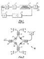
- In a conventional FSK heterodyne system (fig.1) optical signals from the FSK transmitter are demodulated in two steps of optical and electrical demodulation. The transmitted beam is coupled with a beam from a
local oscillator 3 and is converted into an IF signal by means of a square-law detector 5. This produces an electrical IF signal which then is amplified and filtered 7. It is then demodulated to the baseband signal by an IF frequency discriminator 9 and the IF signal passed via abaseband filter 11, IF signal frequency stability is a requisite for stable FSK signal demodulation. It is usual therefore to include afeedback loop amplifier 13, following the discriminator 9, to control the frequency of thelocal oscillator laser 3. A bandwidth for the receiver amplifier, of four times that of the baseband data is usual for this system. - An alternative approach to this is to use a single filter envelope detector having a cut-off midway between the upper and lower signal tones. See Saito et al, "S/N and error rate evaluation for an optical FSK heterodyne system using semiconductor lasers", IEEE Journal of Quantum Electron. 1983 QE-19 pp 180-193. This then has the advantage of a reduced bandwidth, but this is at the expense of a 3dB loss in signal sensitivity.
- The present invention is intended to provide an alternative - an FSK demodulator offering reduced bandwidth but without a corresponding loss in sensitivity.
- In accordance with the invention thus there is provided a frequency shift-keyed (FSK) signal demodulator comprising:-
a local oscillator, for providing a coherent optical reference signal of frequency midway between signal tones;
an optical multiport junction, coupled to the local oscillator and responsive to an optical input signal, for providing combinations of the reference signal and the input signal at the output ports thereof;
detecting means, co-operative with the output ports of the multiport junctions, to produce a plurality of phase-diverse electrical signals at beat frequency in response to the combined optical signals directed thereto; and,
phase discriminating means, co-operative with the detecting means, to produce a demodulated signal the amplitude of which is determined in dependence upon the lead/lag phase relationship of said electrical signals. - The phase discriminating means aforementioned may be either synchronous or asynchronous. The latter does not require frequency-lock circuitry, is therefore less expensive to implement, can be of simple design and is thus preferred. In this latter case, discrimination may involve either mixing or envelope detection.
- In multiport detection as aforesaid the signal and local oscillator are combined in the multiport junction to produce, in general, more than two outputs. Provided that they are combined with suitable phase diversity, then it is possible to determine their relative phase and amplitude. In the limit of a strong local oscillator, photocurrents developed at the output ports become, apart from a large constant term due to the local oscillator power, proportional to the components of signal complex amplitude in directions determined by the phase diversity introduced by the multiport. For a 3x3 multiport implementation with symmetrical coupling, the three photocurrents provide three signals, A, B and C given by


where as is the signal amplitude and ϑ is the phase of the signal relative to a zero set by the local oscillator and choice of optical reference planes. For a balanced 4x4 multiport implementation the detectors provide four photocurrents of which complementary pairs can be combined to give the in-phase component of the signal relative to the local oscillator and the quadrature component.
Writing these as I and Q gives

- Measurement of A, B and C or I and Q gives complete knowledge of the complex amplitude of the signal relative to the local oscillator, namely as and ϑ. Where here the local oscillator and signal are independent, ϑ will change at the beat frequency between them. In this heterodyne detection scheme ϑ thus rotates at this intermediate freqency (IF). With FSK, an advantage of multiport detection is that it is possible to distinguish between positive and negative intermediate frequencies by observing the direction of this rotation of ϑ. The optical local oscillator frequency is set midway between the two signal tones so that this direction of rotation provides a discriminant for the transmitted data. For minimum spacing of the two signal tones the required bandwidth of each detector individually is twice the base bandwidth, rather than four times the base bandwidth required in conventional FSK detection. This reduction of bandwidth is important for high bit rate systems since large bandwidth is difficult to achieve with low noise pre-amplifiers. This multiport approach also has the advantage that it does not suffer the 3dB sensitivity penalty inherent to the reduced bandwidth single filter detection system mentioned earlier.
- In the drawings accompanying this specification:-
- Figure 1 is a block diagram showing the arrangement of a conventional form of an FSK heterodyne demodulation system;
- Figure 2 is a block diagram showing the arrangement of a 4x4 multiport junction of fibre construction;
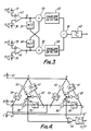
- Figure 3 is a block diagram of an electrical processing circuit, using envelope detection, for use in combination with the multiport junction of figure 2 and in accord with this invention; and,
- Figure 4 is a block diagram of an electrical processing circuit, also using envelope detection for use in combination with a 3x3 multiport junction, also in accord with this invention.
- So that this invention may be better understood, embodiments thereof will now be described and reference will be made to figures 2 to 4 of the accompanying drawings. The description that follows is given by way of example only.
- A 4x4 multiport junction implementation is shown in figures 2 and 3. It is convenient to use a 4x4
balanced multiport junction 15 of optical fibre construction e.g. as shown in figure 2. Thisjunction 15 comprises a network of four2x2 fibre couplers phase delay units 25 and 27 have been inserted to allow adjustment of phase to provide the requisite balance. In the other two arms a pair ofpolarisation controllers 29 and 31 have also been inserted. A local oscillator,laser 3, is connected to one input port of themultiport junction 15, to act as a source of reference signal. Input optical signal I/P, from an FSK transmitter, is coupled to another appropriate input port. The remaining two input ports are not used. Different phase combinations of the input and reference optical signals are directed tophotodiodes junction 15. - The electrical processing part of this implementation is shown in figure 3.
Phase discrimination is provided by envelope detection in the manner illustrated. Each of the signals, the in-phase signal I and the quadrature signal Q is passed via a π/2 phase delay (intermediate frequency) component 49, 51 to a corresponding summingnode node rectifier subtractive node 61. The demodulated signal, produced at thisnode 61, is then passed via abaseband filter 47 to output O/P. - By comparison with the 3x3 junction implementation to be discussed below, it will be seen that the above electrical processing circuitry is more straightforward and requires thus fewer components for implementation. However, the optical part - the 4x4 multiport junction is less straightforward as it requires careful adjustment etc. to ensure the requisite balance conditions. The 3x3 multiport junction is easier to produce and is readily available as a conventional commercial product. Details of electrical asynchronous discriminating circuits suitable for use with this junction will be discussed. In the 3x3 multiport implementations discussed below, the three photocurrents A, B and C have the form of a three-phase a.c. signal at the intermediate frequency (IF). The phase sequence ABC or ACB will depend upon the frequency state, the upper or lower tone of the FSK modulated optical signal that is applied.
- In the arrangement shown in figure 4, an envelope detection arrangement, the photocurrents A, B and C are referred to a pair of
phase discriminating networks 77 and 79. The signals produced at the output of each of thesenetworks 77 and 79 are then substracted by means of adifference amplifier 81 and the demodulated signal produced is baseband filtered 47. Each likenetwork 77 and 79 comprises three symmetrically disposed summingnodes corresponding delay component nodes nodes delay components node diode network 99 to produce input signals for thedifference amplifier 81. It will be noted that the phase connections to these twocircuits 77 and 79 are reversed. Thus for one circuit 77, the photocurrents B and C are referred to input junctions Y and Z whilst for theother circuit 79, these photocurrents B and C are reversed and thus referred to input junctions Z and Y. One circuit will produce maximum output when the phase sequence is in the order ABC, whilst the other circuit will produce maximum output when the phase sequence is reversed, i.e. ACB. - In the foregoing arrangements, the local oscillator frequency (f) is maintained at a frequency (f₀) that is precisely midway between the two FSK tones (f₀ + δf). To this end the optical transmission signal can be coded to provide bursts of frequency lock information to preceed each batch of data. This information can have the form of a train of evenly spaced high-tone and low-tone pulses. Frequency lock can then be attained by maximising the power through the pass band filter when the train of evenly spaced (f₀ + δf) and (f₀ - δf) pulses is passed with δf well out on the wings of the pass-band. Thus if f=f₀ then the output is:-

But when out-of-lock (ie. f≠f₀), the changes in error signal output would be proportional to:-

ie. α -2(f-f₀)².
So that the output is indeed a maximum when f-f₀. Other control circuits, to lock the local oscillator on track are not preceeded from the general scope of this invention.
Claims (5)
- A frequency shift keyed (FSK) optical signal demodulator comprising:-
a local oscillator (3), for providing a coherent optical reference signal (10) of frequency midway between signal tones; an optical multiport junction (15), coupled to the local oscillator (3) and responsive to an optical input signal (I/P), for providing combinations of the reference signal (10) and the input signal (I/P) at the output ports thereof; detecting means(33, 35, 37, 39; 63, 65, 67), co-operative with the output ports of the multiport junction (15), to produce a plurality of phase-diverse electrical signals at beat frequency in response to the combined optical signals directed thereto; and
phase discriminating means (fig. 3; fig. 4;), co-operative with the detecting means (33, 35, 37, 39; 63, 65, 67), to produce a demodulated signal (O/P) the amplitude of which is determined in dependance upon the lead/lag phase relationship of said electrical signals. - An FSK demodulator (figs. 2 and 3;), as claimed in claim 1, comprising:-
a 4x4 multiport junction (15);
a corresponding set of four photodetectors (33, 35, 37, & 39) connected in pairs (33 and 35, 37 and 39) to first and second difference amplifiers (41, 43) respectively, to produce in-phase and quadrature electrical signals (I,Q); and,
phase discriminating means (49-61)to produce the demodulated signal in dependance upon the lead/lag phase relationship of these two electrical signals. - An FSK demodulator (figs. 2 and 3), as claimed in claim 2, wherein the phase discriminating means comprises a delay-and-add network (49, 51, 53, 55) to produce quadrature phase shifted combinations of the in-phase and quadrature electrical signals, an envelope detector (57, 59) responsive to each network output, and a subtractive node (61) connected to the output of each envelope detector (57, 59).
- An FSK demodulator, as claimed in claim 1, comprising a 3x3 multiport junction;
a corresponding set of three photodetectors (63, 65, 67), one at each output port of the junction; and
phase discriminating means (fig. 4) to produce the demodulated signal in dependance upon the phase sequence of the current outputs in the photodetectors (63, 65, 67). - An FSK demodulator (fig. 4), as claimed in claim 4, wherein the phase discriminating means comprises a pair of like delay-add-and-rectify networks (77, 79); and, a difference amplifier (81) connected to both networks (77, 79).
Applications Claiming Priority (2)
| Application Number | Priority Date | Filing Date | Title |
|---|---|---|---|
| GB868625416A GB8625416D0 (en) | 1986-10-23 | 1986-10-23 | Optical fsk demodulator |
| GB8625416 | 1986-10-23 |
Publications (3)
| Publication Number | Publication Date |
|---|---|
| EP0265278A2 EP0265278A2 (en) | 1988-04-27 |
| EP0265278A3 EP0265278A3 (en) | 1989-07-26 |
| EP0265278B1 true EP0265278B1 (en) | 1992-12-30 |
Family
ID=10606208
Family Applications (1)
| Application Number | Title | Priority Date | Filing Date |
|---|---|---|---|
| EP87309388A Expired EP0265278B1 (en) | 1986-10-23 | 1987-10-23 | Optical fsk demodulator |
Country Status (6)
| Country | Link |
|---|---|
| US (1) | US4887314A (en) |
| EP (1) | EP0265278B1 (en) |
| JP (1) | JP2527768B2 (en) |
| AU (1) | AU602015B2 (en) |
| DE (1) | DE3783320T2 (en) |
| GB (2) | GB8625416D0 (en) |
Families Citing this family (12)
| Publication number | Priority date | Publication date | Assignee | Title |
|---|---|---|---|---|
| EP0298484B2 (en) * | 1987-07-10 | 1995-07-12 | Siemens Aktiengesellschaft | Optical FSK homodyne receiver |
| JPH02162330A (en) * | 1988-12-16 | 1990-06-21 | Hitachi Ltd | Polarization diversity optical reception method and device and intermediate frequency stabilization method |
| JP2809796B2 (en) * | 1990-03-14 | 1998-10-15 | 松下電器産業株式会社 | Coherent optical transmission equipment |
| DE4103687C2 (en) * | 1991-02-07 | 1995-02-02 | Kathrein Werke Kg | Phase locked loop for demodulation |
| GB2257319B (en) * | 1991-06-27 | 1995-01-18 | Northern Telecom Ltd | Direct demodulation of optical binary fsk signals |
| JP2824875B2 (en) * | 1991-07-16 | 1998-11-18 | 科学技術振興事業団 | Optical demodulator |
| EP2367034A1 (en) * | 2010-03-16 | 2011-09-21 | Telefonaktiebolaget L M Ericsson (Publ) | Planar waveguide circuit comprising a 90 degree optical hybrid and optical receiver |
| US10126498B1 (en) * | 2017-07-25 | 2018-11-13 | Elenion Technologies, Llc | Optical hybrid |
| US10731383B2 (en) * | 2018-08-01 | 2020-08-04 | Macom Technology Solutions Holdings, Inc. | Symmetric coherent optical mixer |
| JP7227484B2 (en) * | 2019-04-17 | 2023-02-22 | 日本電信電話株式会社 | Optical 90 degree hybrid circuit |
| JP7380329B2 (en) * | 2020-02-28 | 2023-11-15 | 富士通オプティカルコンポーネンツ株式会社 | Optical circuit devices and optical receivers |
| US11333831B2 (en) * | 2020-09-21 | 2022-05-17 | Ii-Vi Delaware, Inc. | Optical couplers and hybrids |
Family Cites Families (6)
| Publication number | Priority date | Publication date | Assignee | Title |
|---|---|---|---|---|
| GB2101821B (en) * | 1981-07-16 | 1984-11-14 | Standard Telephones Cables Ltd | Radio receiver for frequency shift keyed signals |
| US4612509A (en) * | 1983-01-13 | 1986-09-16 | Paradyne Corporation | Frequency shift keyed demodulator |
| NL8401347A (en) * | 1984-04-27 | 1985-11-18 | Philips Nv | A FSK DATA RECEIVER. |
| GB2158330A (en) * | 1984-04-30 | 1985-11-06 | Philips Electronic Associated | An afc system for a direct modulation fm data receiver |
| GB2172766B (en) * | 1985-03-21 | 1988-12-21 | Stc Plc | Optical receiver |
| US4718120A (en) * | 1986-11-24 | 1988-01-05 | American Telephone And Telegraph Company, At&T Bell Laboratories | Polarization insensitive coherent lightwave detector |
-
1986
- 1986-10-23 GB GB868625416A patent/GB8625416D0/en active Pending
-
1987
- 1987-10-23 DE DE8787309388T patent/DE3783320T2/en not_active Expired - Fee Related
- 1987-10-23 EP EP87309388A patent/EP0265278B1/en not_active Expired
- 1987-10-23 JP JP62268009A patent/JP2527768B2/en not_active Expired - Lifetime
- 1987-10-23 GB GB8724860A patent/GB2198904B/en not_active Expired - Lifetime
- 1987-10-23 AU AU80114/87A patent/AU602015B2/en not_active Expired - Fee Related
-
1989
- 1989-02-16 US US07/312,591 patent/US4887314A/en not_active Expired - Fee Related
Also Published As
| Publication number | Publication date |
|---|---|
| JP2527768B2 (en) | 1996-08-28 |
| AU8011487A (en) | 1988-04-28 |
| US4887314A (en) | 1989-12-12 |
| GB8724860D0 (en) | 1987-11-25 |
| DE3783320T2 (en) | 1993-04-22 |
| DE3783320D1 (en) | 1993-02-11 |
| EP0265278A2 (en) | 1988-04-27 |
| GB2198904B (en) | 1991-02-13 |
| GB8625416D0 (en) | 1987-02-04 |
| GB2198904A (en) | 1988-06-22 |
| JPS63164542A (en) | 1988-07-07 |
| AU602015B2 (en) | 1990-09-27 |
| EP0265278A3 (en) | 1989-07-26 |
Similar Documents
| Publication | Publication Date | Title |
|---|---|---|
| EP0198239B1 (en) | Optical receiver | |
| Davis et al. | Phase diversity techniques for coherent optical receivers | |
| EP0445943B1 (en) | Polarization independent coherent lightwave detection arrangement | |
| EP0268741B1 (en) | Polarization insensitive coherent lightwave detector | |
| EP3075083B1 (en) | Polarisation-independent coherent optical receiver | |
| US4887314A (en) | Optical FSK demodulator | |
| US5146359A (en) | Double-stage phase-diversity receiver | |
| WO1986007513A1 (en) | Coherent optical receivers | |
| JPH01117434A (en) | Optical communication system for four value fsk | |
| EP0325281A2 (en) | Optical transmitter, optical receiver and optical transmission apparatus and control method of optical receiver | |
| JPH0478251A (en) | Demodulator and polarized wave diversity receiver for coherent optical communication provided with the demodulator | |
| US7085501B1 (en) | Coherent optical receiver | |
| EP0245026B1 (en) | Optical heterodyne mixers providing image-frequency rejection | |
| CA1308440C (en) | Optical receiving method utilizing polarization diversity and apparatus for carrying out the same | |
| Noe et al. | New FSK phase-diversity receiver in a 150 Mbit/s coherent optical transmission system | |
| JPH0522354A (en) | Optical communication system | |
| Okoshi et al. | Double-stage phase-diversity optical receiver: analysis and experimental confirmation of the principle | |
| JPH07283793A (en) | Coherent optical transmission system | |
| JPH0285830A (en) | Coherent light receiving system | |
| JPH0267831A (en) | optical receiver | |
| JPS63198425A (en) | Intermediate frequency stabilization method | |
| JPH03259632A (en) | Optical heterodyne polarized wave diversity receiver | |
| JPS63200631A (en) | Optical communication method using optical heterodyne detection |
Legal Events
| Date | Code | Title | Description |
|---|---|---|---|
| PUAI | Public reference made under article 153(3) epc to a published international application that has entered the european phase |
Free format text: ORIGINAL CODE: 0009012 |
|
| AK | Designated contracting states |
Kind code of ref document: A2 Designated state(s): DE FR NL |
|
| PUAL | Search report despatched |
Free format text: ORIGINAL CODE: 0009013 |
|
| RAP1 | Party data changed (applicant data changed or rights of an application transferred) |
Owner name: GEC PLESSEY TELECOMMUNICATIONS LIMITED |
|
| AK | Designated contracting states |
Kind code of ref document: A3 Designated state(s): DE FR NL |
|
| 17P | Request for examination filed |
Effective date: 19891211 |
|
| 17Q | First examination report despatched |
Effective date: 19920408 |
|
| RAP1 | Party data changed (applicant data changed or rights of an application transferred) |
Owner name: GPT LIMITED |
|
| GRAA | (expected) grant |
Free format text: ORIGINAL CODE: 0009210 |
|
| AK | Designated contracting states |
Kind code of ref document: B1 Designated state(s): DE FR NL |
|
| ET | Fr: translation filed | ||
| REF | Corresponds to: |
Ref document number: 3783320 Country of ref document: DE Date of ref document: 19930211 |
|
| PLBE | No opposition filed within time limit |
Free format text: ORIGINAL CODE: 0009261 |
|
| STAA | Information on the status of an ep patent application or granted ep patent |
Free format text: STATUS: NO OPPOSITION FILED WITHIN TIME LIMIT |
|
| 26N | No opposition filed | ||
| PGFP | Annual fee paid to national office [announced via postgrant information from national office to epo] |
Ref country code: FR Payment date: 19951010 Year of fee payment: 9 |
|
| PGFP | Annual fee paid to national office [announced via postgrant information from national office to epo] |
Ref country code: NL Payment date: 19951024 Year of fee payment: 9 |
|
| PGFP | Annual fee paid to national office [announced via postgrant information from national office to epo] |
Ref country code: DE Payment date: 19951026 Year of fee payment: 9 |
|
| PG25 | Lapsed in a contracting state [announced via postgrant information from national office to epo] |
Ref country code: NL Effective date: 19970501 |
|
| PG25 | Lapsed in a contracting state [announced via postgrant information from national office to epo] |
Ref country code: FR Effective date: 19970630 |
|
| NLV4 | Nl: lapsed or anulled due to non-payment of the annual fee |
Effective date: 19970501 |
|
| PG25 | Lapsed in a contracting state [announced via postgrant information from national office to epo] |
Ref country code: DE Effective date: 19970701 |
|
| REG | Reference to a national code |
Ref country code: FR Ref legal event code: ST |