EP0264945A2 - Multichamber plasma etching system - Google Patents
Multichamber plasma etching system Download PDFInfo
- Publication number
- EP0264945A2 EP0264945A2 EP87115508A EP87115508A EP0264945A2 EP 0264945 A2 EP0264945 A2 EP 0264945A2 EP 87115508 A EP87115508 A EP 87115508A EP 87115508 A EP87115508 A EP 87115508A EP 0264945 A2 EP0264945 A2 EP 0264945A2
- Authority
- EP
- European Patent Office
- Prior art keywords
- wafer
- vessels
- wafers
- plasma
- plural
- Prior art date
- Legal status (The legal status is an assumption and is not a legal conclusion. Google has not performed a legal analysis and makes no representation as to the accuracy of the status listed.)
- Granted
Links
Images


Classifications
-
- H—ELECTRICITY
- H01—ELECTRIC ELEMENTS
- H01L—SEMICONDUCTOR DEVICES NOT COVERED BY CLASS H10
- H01L21/00—Processes or apparatus adapted for the manufacture or treatment of semiconductor or solid state devices or of parts thereof
- H01L21/02—Manufacture or treatment of semiconductor devices or of parts thereof
- H01L21/04—Manufacture or treatment of semiconductor devices or of parts thereof the devices having at least one potential-jump barrier or surface barrier, e.g. PN junction, depletion layer or carrier concentration layer
- H01L21/18—Manufacture or treatment of semiconductor devices or of parts thereof the devices having at least one potential-jump barrier or surface barrier, e.g. PN junction, depletion layer or carrier concentration layer the devices having semiconductor bodies comprising elements of Group IV of the Periodic System or AIIIBV compounds with or without impurities, e.g. doping materials
- H01L21/30—Treatment of semiconductor bodies using processes or apparatus not provided for in groups H01L21/20 - H01L21/26
- H01L21/302—Treatment of semiconductor bodies using processes or apparatus not provided for in groups H01L21/20 - H01L21/26 to change their surface-physical characteristics or shape, e.g. etching, polishing, cutting
-
- H—ELECTRICITY
- H01—ELECTRIC ELEMENTS
- H01L—SEMICONDUCTOR DEVICES NOT COVERED BY CLASS H10
- H01L21/00—Processes or apparatus adapted for the manufacture or treatment of semiconductor or solid state devices or of parts thereof
- H01L21/67—Apparatus specially adapted for handling semiconductor or electric solid state devices during manufacture or treatment thereof; Apparatus specially adapted for handling wafers during manufacture or treatment of semiconductor or electric solid state devices or components ; Apparatus not specifically provided for elsewhere
- H01L21/67005—Apparatus not specifically provided for elsewhere
- H01L21/67011—Apparatus for manufacture or treatment
- H01L21/67155—Apparatus for manufacturing or treating in a plurality of work-stations
- H01L21/67161—Apparatus for manufacturing or treating in a plurality of work-stations characterized by the layout of the process chambers
- H01L21/67167—Apparatus for manufacturing or treating in a plurality of work-stations characterized by the layout of the process chambers surrounding a central transfer chamber
-
- H—ELECTRICITY
- H01—ELECTRIC ELEMENTS
- H01L—SEMICONDUCTOR DEVICES NOT COVERED BY CLASS H10
- H01L21/00—Processes or apparatus adapted for the manufacture or treatment of semiconductor or solid state devices or of parts thereof
- H01L21/67—Apparatus specially adapted for handling semiconductor or electric solid state devices during manufacture or treatment thereof; Apparatus specially adapted for handling wafers during manufacture or treatment of semiconductor or electric solid state devices or components ; Apparatus not specifically provided for elsewhere
- H01L21/67005—Apparatus not specifically provided for elsewhere
- H01L21/67011—Apparatus for manufacture or treatment
- H01L21/67017—Apparatus for fluid treatment
- H01L21/67063—Apparatus for fluid treatment for etching
- H01L21/67069—Apparatus for fluid treatment for etching for drying etching
-
- H—ELECTRICITY
- H01—ELECTRIC ELEMENTS
- H01L—SEMICONDUCTOR DEVICES NOT COVERED BY CLASS H10
- H01L21/00—Processes or apparatus adapted for the manufacture or treatment of semiconductor or solid state devices or of parts thereof
- H01L21/67—Apparatus specially adapted for handling semiconductor or electric solid state devices during manufacture or treatment thereof; Apparatus specially adapted for handling wafers during manufacture or treatment of semiconductor or electric solid state devices or components ; Apparatus not specifically provided for elsewhere
- H01L21/67005—Apparatus not specifically provided for elsewhere
- H01L21/67011—Apparatus for manufacture or treatment
- H01L21/67126—Apparatus for sealing, encapsulating, glassing, decapsulating or the like
-
- H—ELECTRICITY
- H01—ELECTRIC ELEMENTS
- H01L—SEMICONDUCTOR DEVICES NOT COVERED BY CLASS H10
- H01L21/00—Processes or apparatus adapted for the manufacture or treatment of semiconductor or solid state devices or of parts thereof
- H01L21/67—Apparatus specially adapted for handling semiconductor or electric solid state devices during manufacture or treatment thereof; Apparatus specially adapted for handling wafers during manufacture or treatment of semiconductor or electric solid state devices or components ; Apparatus not specifically provided for elsewhere
- H01L21/67005—Apparatus not specifically provided for elsewhere
- H01L21/67011—Apparatus for manufacture or treatment
- H01L21/67155—Apparatus for manufacturing or treating in a plurality of work-stations
- H01L21/6719—Apparatus for manufacturing or treating in a plurality of work-stations characterized by the construction of the processing chambers, e.g. modular processing chambers
-
- H—ELECTRICITY
- H01—ELECTRIC ELEMENTS
- H01L—SEMICONDUCTOR DEVICES NOT COVERED BY CLASS H10
- H01L21/00—Processes or apparatus adapted for the manufacture or treatment of semiconductor or solid state devices or of parts thereof
- H01L21/67—Apparatus specially adapted for handling semiconductor or electric solid state devices during manufacture or treatment thereof; Apparatus specially adapted for handling wafers during manufacture or treatment of semiconductor or electric solid state devices or components ; Apparatus not specifically provided for elsewhere
- H01L21/67005—Apparatus not specifically provided for elsewhere
- H01L21/67242—Apparatus for monitoring, sorting or marking
- H01L21/67276—Production flow monitoring, e.g. for increasing throughput
-
- H—ELECTRICITY
- H01—ELECTRIC ELEMENTS
- H01L—SEMICONDUCTOR DEVICES NOT COVERED BY CLASS H10
- H01L21/00—Processes or apparatus adapted for the manufacture or treatment of semiconductor or solid state devices or of parts thereof
- H01L21/67—Apparatus specially adapted for handling semiconductor or electric solid state devices during manufacture or treatment thereof; Apparatus specially adapted for handling wafers during manufacture or treatment of semiconductor or electric solid state devices or components ; Apparatus not specifically provided for elsewhere
- H01L21/677—Apparatus specially adapted for handling semiconductor or electric solid state devices during manufacture or treatment thereof; Apparatus specially adapted for handling wafers during manufacture or treatment of semiconductor or electric solid state devices or components ; Apparatus not specifically provided for elsewhere for conveying, e.g. between different workstations
- H01L21/67739—Apparatus specially adapted for handling semiconductor or electric solid state devices during manufacture or treatment thereof; Apparatus specially adapted for handling wafers during manufacture or treatment of semiconductor or electric solid state devices or components ; Apparatus not specifically provided for elsewhere for conveying, e.g. between different workstations into and out of processing chamber
- H01L21/67742—Mechanical parts of transfer devices
-
- Y—GENERAL TAGGING OF NEW TECHNOLOGICAL DEVELOPMENTS; GENERAL TAGGING OF CROSS-SECTIONAL TECHNOLOGIES SPANNING OVER SEVERAL SECTIONS OF THE IPC; TECHNICAL SUBJECTS COVERED BY FORMER USPC CROSS-REFERENCE ART COLLECTIONS [XRACs] AND DIGESTS
- Y10—TECHNICAL SUBJECTS COVERED BY FORMER USPC
- Y10S—TECHNICAL SUBJECTS COVERED BY FORMER USPC CROSS-REFERENCE ART COLLECTIONS [XRACs] AND DIGESTS
- Y10S414/00—Material or article handling
- Y10S414/135—Associated with semiconductor wafer handling
- Y10S414/137—Associated with semiconductor wafer handling including means for charging or discharging wafer cassette
Definitions
- This invention is directed to the field as semiconductor processing, and more particularly, to a novel multiple-processing and contamination-free plasma etching system.
- Plasma etching devices are commonly employed during one or more of the phases of the integrated circuit fabrication process, and are typically available in either a single-wafer or a plural-wafer configuration.
- the single-wafer configurations while providing excellent process control, suffer from a restricted system throughput capability.
- Efforts to relieve the throughput limitations have been generally unsuccessful.
- system utility is limited due to the undesirable phenomenon of resist "popping", notwithstanding that various cooling approaches have been used including clamping, cooling of the wafer underside with a helium flow, and the mixing of helium into the plasma.
- the multiple-wafer configuration while providing a comparatively much-greater system throughput, have been generally subject to less-than-desirable process and quality control. Not only are end-point determinations for each of the multiple wafers either not available or not precisely determinable, but also electrode positional accuracy for different electrode gaps and correspondingly different gas chemistries is often difficult to establish and maintain.
- the single-wafer and the multiple-wafer configurations are both subject to the further disadvantage that two or more step processes typically expose the wafers to an undesirable environment in the intermediate handling step, which materially increases the possibility of wafer contamination, and which further restricts the processing throughput.
- the present invention contemplates plural single-wafer plasma reactors each operative inidividually to provide excellent process control of single wafers, collectively operative to provide a system throughput limited only by the number of the plural plasma reactors, and so cooperative with a common wafer transfer and queuing means as to provide both single-step and multiple-step wafer processing in a manner that neither exposes the wafers to an undesirable atmosphere not to human handling.
- plural plasma reactors and cassettte elevator are symmetrically arrayed about an X, TT movable wafer arm assembly.
- the plural reactors, the cassette elevator, and the X, TT movable wafer arm are maintained in a controlled vacuum condition, and the central S, TT movable wafer arm is in radial communication with the peripherally surrounding plasma reactors and cassette elevator via a corresponding one of a plurality of vacuum lock valves.
- the arm of the R, TT movable wafer arm assembly includes an apertured platform for supporting each wafer, and a cooperative bumper for releasably engaging the back and the periphery of the supported wafer without any wafer front surface contact.
- Each of the plural plasma reactors includes a stationary bottom electrode and a movable upper electrode that are cooperative to provide a variable wafer-cathode to anode gap therebetween of a selectable dimension.
- a support assembly including a micrometer adjustment stop is provided for selectively positioning the movable electrode, and in another embodiment, a combination micrometer stop and pneumatic actuators are provided for selectively positioning the movable electrode.
- a vertically movable pedestal is slidably mounted centrally to the stationary electrode of each of the plural plasma reactors that cooperates with the apertured platform of the R, TT movable wafer arm assembly to load and unload the wafers respectively onto and off of the stationary electrode.
- a reactant gas injection system, a RF power source, and an end-point determination means are operatively coupled to each of the plural plasma reactors.
- the plural plasma reactors are operable in either embodiment to run the same or different processes, and are cooperative with the R, TT movable wafer arm assembly to provide one of the same single-step processing simultaneously in the plural plasma reactors, different single-step processing simultaneously in the plural plasma reactors, and sequential two or more step processing in the plural reactors. Two embodiments of the R, TT movable wafer arm assembly are disclosed.
- FIG. 10 generally designated at 10 is a pictorial diagram illustrating the multiple-processing and contamination-free plasma etching system according to the present invention.
- the system 10 includes a plurality of single-wafer plasma reactors generally designated 12 to be described and a wafer queuing station generally designated 14 to be described that are arrayed about a closed locus as illustrated by a dashed line 16.
- a load/unload module generally designated 18 to be described is disposed concentrically within the plural plasma reactors 12 and the queuing station 14 for singly transferring wafers to be processed and after processing between the queuing station 14 and one or more of the plasma reactors 12.
- a plurality of vacuum locks generally designated 20 to be described are individually provided at the interfaces of the several plasma reactors 12 and the load and unload module 18, and between the interface of the queuing station 14 and the load and unload module 18.
- a processor 22 is operatively coupled to the plural plasma reactors 12, to the queuing station 14, and to the load and unload module 18 for activating and de-energizing radio frequency plasma inducing fields in well-known manner, for controlling and processing in well-known manner the signal output of end-point determination means coupled to the several plasma reactors, and for initiating and coordinating wafer transfer between the several reactors and the queuing station to be described.
- a reactant gas injection system 24 to be described is operatively coupled to the plural plasma reactors 12 for controllably injecting preselected reactants and other process gases severally into the plural plasma reactors.
- a vacuum system 26 is operatively coupled to the reactors 12, to the queuing station 14, and to the load and unload module 18 for maintaining the entire assembly at a controlled vacuum condition during operation.
- the process 22 is operatively coupled to the reactant gas injection system and to the vacuum system 26.
- the several reactors 12, the queuing station 14, and the concentric load and unload module 18 conserve space utilization and in such a way as to provide a comparatively-compact plasma etching system.
- the load and unload module 18 and cooperative ones of the vacuum locks 20 are operable to transfer wafers singly between the queuing station 14 and selected reactors 12 in a single-step processing mode and between selected reactors 12 in a two or more step processing mode without any residual or environmentally-induced wafer contamination as well as without intermediate operator handling.
- the plasma etching system of the present invention is characterized by both an excellent process control and a high processing throughput, the mutual coexistence of both features having not heretofore been possible in a practicable embodiment.
- the queuing station 14 preferably includes a cassette, not shown, having plural vertically-spaced wafers 32 stacked therein.
- the cassette is preferably mounted for vertical stepping motion by an indexed elevator assembly schematically illustrated at 34, that is operable under control of the processor 22 ( Figure 1) to step the cassette in vertical increments that correspond to the spacing of the vertically spaced wafers for addressing the associated cassette slot position. It will be appreciated that in this way individual wafers in the cassette are addressed for removal for processing and for return after processing to their corresponding slot positions.
- any other suitable wafer queuing station can be employed as well without departing from the inventive concept.
- the vacuum locks 20 intermediate the queuing station 14 and the load/unload module 18 and intermediate the plural plasma reactors 12 and the load and unload station 18 each include a housing body generally designated 40.
- the housing 40 includes a plate 42 having opposing top, bottom, and side walls 44 orthogonal thereto that cooperate to define a generally-rectangular hollow generally designated 46 therewithin as best seen in Figure 3A.
- a flange 47 is provided peripherally around the walls 44 on the ends thereof remote from the plate 42, and bolts 48 are provided through the ends of the plate 42 and of the flange 47 for fastening the housing body 40 at the interfaces between corresponding ones of the plasma reactors 12 and the load and unload station 18 and between the interface between the queuing station 14 and the load and unload station 18.
- O-rings 50 are provided on the sealing faces of the plate 42 and flange 47 for providing an air-tight seal.
- An elongated slot generally designated 54 is provided through the plate 47 that is in communication with the generally-rectangular hollow 46.
- a chamber door assembly generally designated 56 is cooperative with the slot 54 to provide a valving action.
- the door assembly 56 includes an elongated, generally-rectangular plate 58 of dimensions selected to be larger than the dimensions of the slot 54.
- An O-ring sealing member 60 is provided in the sealing face of the plate 58 and surrounding the slot 54.
- the plate 58 is fastened to an arm 62 that is mounted for rotary motion with a shaft 64 journaled in spaced bearings 66 that are fastened to the plate 42.
- a chamber door TT-drive actuator is fastened to the shaft 64 through the edge of the housing 40 preferably via a ferrofluidic or other rotary seal as illustrated dashed at 70.
- the chamber door 56 is pivoted by the chamber door TT-drive actuator between an open condition, illustrated in dashed outline in Figures 3A, and a closed condition, illustrated in solid outline in Figures 3A and 3B.
- the generally rectangular hollow 46 is in open communication with the elongated slot 54, so that a wafer arm assembly to be described may readily be moved therethrough between the load and unload station 18 and the several plasma reactors 12 and the queuing station 14.
- the load and unload module is sealed from the plural plasma reactors 12 and from the queuing station 18.
- the load and unload module 18 includes a top wall 72, pentagonally-arranged side walls 74, and a pentagonal bottom wall 76 defining an enclosure generally designated 78.
- a R, TT movable wafer arm assembly generally designated 80 to be described is mounted in the enclosure 78.
- the assembly 80 includes a turntable 82 mounted for TT-rotation with a shaft 84 journaled in a bearing assembly generally designated 86 that is fastened in a central aperture provided therefor in the bottom wall 76.
- a Theta drive motor 88 mounted to the bottom wall 76 is operatively coupled to the shaft 84 via a belt and wheel arrangement generally designated 90.
- the shaft 84 and therewith the turntable 82 rotates to any selected angular TT orientation for aligning the wafer arm assembly 80 with any one of the plasma reactors 12 or with the queuing station 14 at the corresponding TT1, TT2, TT3, TT4, and TT5 coordinates.
- a shaft 92 is concentrically mounted within the shaft 84 and journaled for rotation therein on a bearing and vacuum seal assembly generally designated 93. Any suitable rotary vacuum seal, such as a ferrofluidic rotary vacuum seal, may be employed. On end of the shaft 92 is connected to pivot bearing 94 to be described vacuum-mounted through the turntable 82, and the other end of the shaft 92 is operatively coupled to a R-drive motor 92 via a belt and wheel arrangement generally designated 98.
- the wafer arm of both embodiments of the R, TT movable wafer arm assembly to be described is controllably translated in the R-direction for loading and unloading idividual wafers into and out of the plural reaction chambers 12 and queuing station 14 through the associated vacuum lock 20.
- th wafer arm assembly 80 includes a wafer receiving and releasing paddle assembly generally designated 100.
- the paddle assembly 100 includes a platform 102 having a central opening generally designated 104 therethrough.
- the member 102 terminated in laterally spaced fingers 106 having wafer-periphery engaging upstanding flanges 108 integrally formed on the free ends thereof.
- a releasable abutment generally designated 110 having a bumper portion 112 and an integral tail portion 114 is mounted for sliding motion to the platform member 102.
- a coil spring 116 is mounted between the releasable abutment 110 and the member 102 which urges the bumper 112 in the direction of an arrow 118 so as to abut and therewith frictionally engage the periphery of a wafer, not shown, received between the bumper 112 and the flanges 108.
- the tail 114 includes a downwardly depending stop 120 to be described that is slidably received in an elongated aperture provided therfor in the platform member 102 that is cooperative with an upstanding abutment to be described to release the frictional wafer engagement as the arm reaches its position of maximum extension.
- the paddle assembly 100 is mounted between plates 124 to a carriage assembly generally designated 126 that is slidable mounted on linear bearings 128 that are fastened to end posts 130 upstanding from and fastened to the rotatable turntable 82.
- the carriage 126 is controllably moved in either direction along the linear bearings 128 for loading and unloading wafers individually to and from the several plasma reactors 12 and the queuing station 18.
- a member 131 is pivotally mounted subjacent the carriage 126, which houses therein a linear bearing, not shown.
- a shaft 132 is slidably received through the linear bearing of the pivoting housing 131.
- One end of the shaft 132 is slidably mounted in a sleeve 134 that is mounted for rotary motion to the turntable 82 via a pivot bearing 136, and the other end of the shaft 132 is fastened to a needle bearing assembly 138 that is pivotally fastened to a crank arm 140 mounted for rotation with the shaft 92 of the R-drive motor 96 ( Figure 4) via a mounting coupling 142 fastened to the turntable 82.
- the turntable 82 and therewith the paddle assembly 100 is rotated to that TT coordinate that corresponds to any selected one of the angular locations of the plural plasma reaction chambers designated TT1 through TT4 in Figure 2, and to that TT coordinate that corresponds to the angular location of the wafer queuing station 14 designated TT5 in Figure 2.
- the crank 140 traces an arcuate path as illustrated by an arrow 144.
- the arm 132 therewith pivots on the pivot bearing 136 as shown by an arrow 146, and moves the carriage 126 linearly along the bearings 128 in a direction that corresponds to the sense of rotation of the X-drive motor as illustrated by an arrow 148.
- the arm is either more or less elongated relative to the coupling 136 as it is pivoted by the crank 140, and depending on the sense of the rotation, it slides within the sleeve 134 and within the housing 131 as illustrated by an arrow 150.
- the stop 120 on the tail portion 110 abuts the confronting wall of the upstanding end post 130, such that with continued motion of the paddle along the R direction the bumper 110 draws away from the flanges 108 and thereby releases the frictional engagement of the wafer periphery.
- the wafers are free to be loaded or unloaded to and from any selected plasma reactor 12 and/or are free for pick up or delivery back into the queuing station 14.
- Contacts 156 are mounted to the platform member 102 of the paddle assembly 100 as shown in Figure 7.
- the contacts are operative in response to the presence of a supported wafer to provide a three-point signal indicative of whether or not the wafer is properly seated on the wafer transfer arm.
- the contacts preferably are formed on a printed circuit board, not shown, mounted to the paddle assembly 100. A different number thereof, or other sensing means may be utilized, so long as an accurate indication of intended seating of individual wafers is provided.
- each of the plasma reactors 160 includes a top plate 162, a spaced-apart bottom plate 164 and a cylindrical sidewall 166 cooperate to define a plasma chamber generally designated 168.
- a first electrode generally designated 170 is fastened to the bottom plate 164.
- a pedestal schematically illustrated dashed at 172 is slidably mounted centrally in the bottom electrode 170 for vertical motion with the shaft of a pneumatic cylinder schematically illustrated in dashed outline 174.
- the pedestal 172 is cooperative with the paddle arm assembly to allow for removal and delivery of individual wafers into and out of the plasma chambers.
- the pedestal pneumatic cylinder 174 is driven by a controlled air supply, now shown, operatively coupled thereto via an air input port 176 and an air output port 178.
- a source of colling liquid is coupled to internal fluid flow passageways, not shown, provided through the interior of the bottom electrode 170 via input and output ports 182, 184 for removing the heat produced in the bottom electrode during plasma etching.
- a top electrode generally designated 186 is fastened to a support shaft generally designated 188 that is slidably received through the top plate 162 in a vacuum-tight sealing engagement therewith as by a stainless steel vacuum bellows 190 fastened between the top plate 162 and a superadjacent shaft support plate 187.
- the top electrode 186 includes internal cooling/heating fluid flow passageways schematically illustrated in dashed outline 189 that are coupled via fluid flows conduits 190 disposed in the shaft 188 to a source, not shown, via a liquid input port 194 and an output port 196 provided in the plate assembly 187.
- a pneumatic actuator generally designated 200 having a ram 202 is mounted to the support plate assembly 187.
- the plate 187 moves upwardly, and therewith the shaft 188 and electrode 186 move upwardly and away from the stationary bottom electrode 170.
- micrometer adjustment posts 204 fastened to the plate assembly 187 bear against the top plate 162 and therewith support the top electrode 186 in an intended spaced-apart relation with the bottom electrode 170.
- the gap between the electrodes is adjustable by changing the length of the micrometer adjustment posts selectively. In the preferred embodiment, between 2/16 inch to 2 inches of gap adjustment is provided.
- the shaft 188 has a hollow interior generally designated 206, and a laser window 208 is mounted across the hollow of the shaft 206.
- the beam of an external laser passes through the window and hollow shaft for providing end-point determinations of the plasma etch state.
- Other end-point determination means such as a lateral optical detector, may be employed as well without departing from the inventive concept.
- Reactant gas injection ports 210 are coupled via internal shaft conduits provided therefor, not shown, to a liquid-cooled showerhead gas manifold illustrated in dashed outline 211 in the upper electrode 186. Reactant gas is controllably released therefrom into the plasma reactor, and radio frequency power is applied in the plasma reaction chambers.
- the spacing between the electrodes can be preselected for each particular plasma process, and additional micrometers, in place of the pneumatic actuators 200, can advantageously be employed.
- FIG. 10 generally designated at 212 is a schematic diagram illustrating the presently preferred gas injection and controlled vacuum systems.
- four independently valved sources of gases are respectively connected to individual ones of plasma vessels via corresponding ones of a plurality of gas manifolds, two banks of gas sources generally designated 214, 216 and two manifolds 218, 220 being specifically illustrated.
- a vacuum system 22 is operatively coupled in common to the plural plasma reactor chambers, to the queuing stations 224, and to the load and unload island 226.
- the vacuum system controls the vacuum condition in the entire system, so that the wafers are free from possible contamination as the vacuum locks are severally opened and closed during single and multiple phase processing wafer transfer. It should be noted that while four plasma reactors are disclosed, a greater or a lesser number can be employed without departing from the inventive concept.
- FIG. 11A generally designated at 230 is a perspective view of an alternative embodiment of the X. TT wafer arm assembly according to the present invention.
- the assembly 230 includes a pully 232 mounted for rotation with the shaft of the TT drive motor as best seen in Figure 11B.
- the pulley 232 includes a grooved rim 234 around which a cable 236 is wrapped.
- the cable is drawn tangentally to the grooved rib 234 in opposing directions, and respectively wrapped over pulleys 238, 240 and tied to a slide 242, as best seen at 244 in Figure 11B.
- the slide 242 linearly moves along the linear bearings 246.
- a wafer arm generally designated 248 is mounted for movement with the slide 242 such that the arm 248 is controllably extended and retracted in dependence on the angular position of the pulley 232.
- the ends of the cable preferably are terminated in the slide 242 against resilient biasing elements generally designated 250 in Figure 12.
- the cable 236 as it stretches is pulled in a reverse direction by the resilient couplings 250 for maintaining its intended state.
- the Theta-drive motor turns the turntable of the R, TT wafer arm assembly to the TT coordinate of the queuing station in either embodiment of the R, TT movable wafer arm assembly.
- the vacuum lock of the associated interface is released, and the arm is extended under the wafer in the addressed cassette slot position.
- the arm is then retracted back into the load and unload module, and the vacuum lock is restored.
- the R, TT wafer arm assembly is then rotated to the TT coordinate of the selected plasma reactor.
- the associated chamber door is then rotated to its open condition for providing access to the selected reaction chamber, and the upper electrode is raised.
- the wafer receiving arm is then extended in the R direction through the associated slot valve opening and into the selected reaction chamber.
- the depending stop flange on the wafer arm abuts the upstanding end post on the turntable and, with continued radial motion, the bumper withdraws thereby freeing the wafer from peripheral friction engagement.
- the central pedestal of the lower electrode is then controllably raised by its pneumatic actuator, and therewith the wafer supported on the arm is elevated upwardly off of the wafer support platform. Thereafter, the wafer arm is retracted out of the plasma chamber through the open slot valve and back into the load and unload station. The pedestal is then controllably lowered. The wafer lowers therewith until the pedestal is in its retracted position and the wafer is supported on the surface of the lower electrode.
- the associated chamber door is then closed, and the upper electrode is lowered to that precise preselected gap that implements the particular plasma process being run.
- the intended reactants are then injected through the gas manifold of the upper electrode, the radio frequency power is applied.
- plasma etching of each single wafer is continued until the laser provides a signal indication that the proper end-point has been achieved.
- the RF power is turned-off, the vacuum lock is opended, and the above-described process is repeated, but in reverse order, for removing the wafer out of that plasma chamber and back into the load and unload station.
- the wafer can then be moved into another plasma reactor for a subsequent process in a two or more step processing mode, or back into the cassette in a one-step processing mode.
- the load and unload module, queuing station, and plural reactors are operable in three basic modes, namely, where each reactor is simultaneously performing the same plasma reaction, where each plasma reactor is simultaneously performing two or more different plasma processes, and where the plasma reactors are severally being operated to provide multiple-step processing of single wafers before their return back to the queuing station.
- the wafers are transferred and processed in a controlled vacuum environment such that atmospheric exposure and handling induced contamination are wholly eliminated.
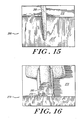
- Figure 13-17 are scanning electron micrographs illustrating exemplary microstructures capable of being formed in a single-step process
- Figure 18 is a scanning electron micrograph illustrating an exemplary microstructure capable of being fabricated in a double-step etch process.
- Figure 13 shows generally at 260 polysilicon with an overlayed photoresist 262 on the surface of the silicon dioxide layer 264 of the wafer.
- CCl4 at 20 sccm and H e at 30 sccm are applied to the plasma reactor at a pressure of 100 mt and a power of 300 watts. The etch occurs for approximately 1 1/2 minutes.
- doped polysilicon 265 having a comparatively high resistivity (30-200 ohms per sq.) and having a slopped profile mask is illustrated.
- SF6 at 50 sccm and freon 115 (C2CIF5) at 50 sccm are controllably injected into a plasma reactor at 150 mt pressure and a 100 watt power. After about 2 1/2 minutes, the illustrated doped polysilicon microstructure is fabricated.
- a trench generally designated 268 is formed in the silicon 272 by injecting BCl3 at 5 sccm and Cl2 at 25 sccm into the plasma reactor at a 100 mt chamber pressure and at 750 watts power for about 20 minutes.
- refractory silcide, TaSi/poly is illustrated generalldy at 274.
- the silicon dioxide surface 276 is overlayed with a polysilicon layer 278 upon which is overlayed the TaSi/poly 280 over which is the photoresist.
- the microstructure is fabricated by injecting CCl4 at 20 sccm and He at 30 sccm into a plasma reactor maintained at a chamber pressure of 80 mt and a radio frequency power of 300 watts for about 3 1/2 minutes.
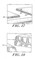
- FIG 17 generally designated 282 is another microstructure exemplary of the single-step structures capable of being fabricated by the contamination-free and multiple-processing plasma reactor of the present invention.
- a photoresist 284 is layed over an aluminum and silicon layer 286 which is overlayed via a TiW layer 288 on the wafer surface.
- the illustrated structure was fabricated by injecting BCl3 at 50 sccm with Cl2 at 15 sccm into the plasma reactor maintained at 125 mt chamber pressure and a 300 watt RF power for about 2 1/2 to 3 1/2 minutes.
- FIG. 18 generally designated at 290 is a silicon dioxide/poly/silicon dioxide/poly sandwich structure illustrating an exemplary two-step process.
- a poly layer designated poly 1 and an oxide layer designed oxide are formed after etching with C2F6 at 100 sccm at a 700 mt pressure and a 600 watt radio frequency power in a first chamber.
- the upper poly 2 layer and the oxide and an overlayed photoresist layer are formed by a separate step employing CCl4 at 20 sccm and He at 30 sccm in a second reaction chamber maintained at a 100 militore chamber pressure and a 600 watt radio frequency power.
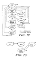
- FIG. 19 illustrates a state diagram for overall system operation.
- system initialization procedures are accomplished which take the system from a turn-on state through necessary warm-ups and start up proceedures.
- Transition to a subsequent state 302 occurs once the system initialization has been completed.
- State 302 exists until a cassette has been placed into the cassette queue station and all door interlock switches are activated.
- the transition from the determine ready state 302 to a machine initialization state 304 occurs once these conditions have been met and the operator initiates system operation through a start button, provided no other system interrupt signals or hold designations have occurred and provided the user has not activated the diagnostic state 306 which is alternatively entered from the determine ready state 302.
- the diagnostic state 306 runs a set of diagnostics on the system should that state be entered by the user. Otherwise, the machine initialization state 304 accomplishes a final set of system power-ons, gas perge or other initialization steps which would not normally be entered in the system initialization state 300 for time and/or power considerations.
- a standby state 306 may be entered by operator designation through a standby button which effectively aborts the processing steps back to the determine ready state 302. Otherwise, from the machine initialization state 304, once the initialization functions have been completed, the system transitions to a cassette pump down state 310 in which a vacuum is drawn from the wafer queuing station 14 placing it into the environment of the transport arm and plural etch vessels. After pump down of the wafer queuing station 14, state 310 processing will normally transition to the state 312 in which the wafers and the cassette at the queuing station 14 are processed in sequence as illustrated in the subsequent figures.
- the system processes each wafer in the cassette according to a wafer command list entered into the system and described below. Once that cycle is complete, processing proceeds to a state 316 which vents the wafer queuing station 14 and waits until removal of the cassette at which point the system transitions to state 300.
- the operation within the cassette process state 312 follows a flexible processes control illustrated in the flow diagram of Figure 20. As illustrated there processing proceeds between state 320 labeled slots, state 322 labeled wafers, state 324 labeled wafer commands, and state 326 labeled machine monitors.
- the processing of Figure 20 is initiated when the state 312 is entered with a cassette of unprocessed wafers, and starts, and finishes, in state 320.
- State 320 initiates a wafer start command for each slot containing an unprocessed wafer using, for example, a top to bottom priority scheme, or any other priority scheme which may be programmed. From the state 320 for a selected slot, and corresponding wafer, processing proceeds to the wafer state 322.
- the processing commands or specifications for each wafer are accessed in a subsequent state 324, wafer commands.
- the wafer commands will be programmed into the system corresponding to the desired processing of each wafer, for example, one or more etches for a designated time period or depth in a designated gas.
- the commands in the state 324 are executed in sequence, and each command commences a set of machine control operations which occur in state 326, machine monitors.
- processing returns to the wafer command state 324 to execute another wafer command.
- processing returns to the state 322 and from thence to state 320 thereby sequencing through the wafers and the cassette slots.
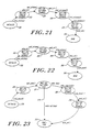
- Processing within the machine control state 326 is in accordance with the wafer transport algorithms of Figs. 21, 22 and 23 and the internal chamber or vessel processing algorithm of Fig. 24. In each case where processing halts for receipt of system instructions to proceed, processor state evaluation checks for existence conditions necessary for the unit to proceed to the next step.
- Fig. 21 illustrates processing for moving a wafer from one chamber or vessel to another, in accordance with wafer commands specifying multiple chamber or vessel processing.
- processing commences at initialization state 330.
- Subsequent state 332 directs the transport arm wafer support table from one chamber or vessel to the desired chamber or vessel wherein the wafer to be moved is located. Once that positioning is accomplished a subsequent state 334 activates the valve and arm mechanisms in a transition to a state 336.
- state 336 the system repositions the transport arm wafer support table to the destination chamber or vessel and transitions to a state 338 which, when it receives control signals, activates the arm mechanism and valving on the applicable chamber to place the wafer in that particular chamber in the transition to a state 340.
- state 340 the wafer relocation function is complete and processing returns to the next wafer command in state 324.
- Fig. 22 illustrates the processing wherein a wafer is moved from a chamber or etch vessel to a slot of the cassette.
- processing transitions to a state 352 which awaits the direction of the transport arm wafer support table to the desired chamber having the wafer to be returned to the cassette.
- state 352 Once the proper positioning is accomplished, the transition from state 352 to state 354 sends a request to the command list asking to be instructed to remove the wafer from the chamber.
- the transition to state 356 executes the machine instruction to open the valves and move the transport arm to pick up the wafer in the chamber and extract it from the chamber or vessel and in addition to request from the wafer command list the instructions to move to the cassette.
- the system transitions to state 358 and sends a request to the wafer processing list for instructions to place the wafer into the cassette and identified slot.
- the transition to the done state 360 executes the wafer insertion into the cassettes slot and returns processing back to the algorithm of Fig. 20.
- Fig. 23 illustrates the algorithm for transferring a wafer from the cassette to a designated chamber in accordance with instructions in the wafer command list.
- processing transitions to a state 372 in which the request is sent to the command list for instructions to position the arm to the cassette and such arm manipulation is executed.
- state 374 transitions to state 374 in which a request for the instructions to extract a wafer from the cassette is sent.
- the state 374 has two possible outcomes, in the first represented by branch 376, a wafer is not found in the slot in which the system has been instructed to retrieve it by the transport arm. In this case the system transitions to a done state 378 indicating that the algorithm of Fig.
- state 374 the wafer is found and the system transitions from state 374 to state 380 in which instructions are received from the wafer processing list to position the transport arm support table at the destination chamber or vessel.
- state 380 that destination chamber is reached, the system transitions to a state 382 in which the system requests and receives instructions from the command list (if the chamber is ready) to insert that wafer into the chamber.
- the mechanisms of the arm and the chamber valving are activated in order to install the wafer into the chamber.
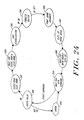
- Fig. 24 illustrates the processing of the system for accomplishing wafer etching within a chamber to which the system has allocated a wafer from the cassette at the queuing station.
- Fig. 24 The processing of Fig. 24 is initiated by a start command obtained from the command list which initiates a state 390.
- the state 390 loops through an error recognition state 392 to a start command wait step 394 if the start command is determined to have incorrect signature. Otherwise, processing from a state 390 proceeds to a state 392 in which the valve to the chamber is sealed and the electrode spacing set to the etch condition.
- a subsequent step 394 waits for confirmation signals from microswitches indicating proper gate closure and electrode positioning.
- a state 396 commences the flow of a gas, selected from the wafer command list, for the desired processing and waits for a steady state gas condition, based on time or other factors, to occur.
- a transition to a state 398 activates the RF plasma generation between the electrodes used for plasma etching within the gas and wafer processing by gas vapor etch continues until a parameter indicating complete processing is obtained.
- a parameter may be a function of time, detected etch depth, or other factors.
- the transition from state 398 to state 400 deactivates the RF and in state 400 the gas environment in the chamber is evacuated so that, in subsequent state 402, the electrodes can be respaced for wafer removal, and the gate or chamber doors opened to the environment of the transport arm without fear of leaking reactor gas into that environment.
- State 402 transitions to state 404 in which the system awaits confirmation by microswitch activation of proper electrode spacing and opening and transitions to state 394 in which system processing returns to the flexible process control of Fig. 20.
Abstract
Description
- This invention is directed to the field as semiconductor processing, and more particularly, to a novel multiple-processing and contamination-free plasma etching system.
- Plasma etching devices are commonly employed during one or more of the phases of the integrated circuit fabrication process, and are typically available in either a single-wafer or a plural-wafer configuration. The single-wafer configurations, while providing excellent process control, suffer from a restricted system throughput capability. Efforts to relieve the throughput limitations, have been generally unsuccessful. For these high-temperature etching processes, system utility is limited due to the undesirable phenomenon of resist "popping", notwithstanding that various cooling approaches have been used including clamping, cooling of the wafer underside with a helium flow, and the mixing of helium into the plasma. The multiple-wafer configuration, while providing a comparatively much-greater system throughput, have been generally subject to less-than-desirable process and quality control. Not only are end-point determinations for each of the multiple wafers either not available or not precisely determinable, but also electrode positional accuracy for different electrode gaps and correspondingly different gas chemistries is often difficult to establish and maintain. The single-wafer and the multiple-wafer configurations are both subject to the further disadvantage that two or more step processes typically expose the wafers to an undesirable environment in the intermediate handling step, which materially increases the possibility of wafer contamination, and which further restricts the processing throughput.
- The present invention contemplates plural single-wafer plasma reactors each operative inidividually to provide excellent process control of single wafers, collectively operative to provide a system throughput limited only by the number of the plural plasma reactors, and so cooperative with a common wafer transfer and queuing means as to provide both single-step and multiple-step wafer processing in a manner that neither exposes the wafers to an undesirable atmosphere not to human handling.
- In the preferred embodiment, plural plasma reactors and cassettte elevator are symmetrically arrayed about an X, TT movable wafer arm assembly. The plural reactors, the cassette elevator, and the X, TT movable wafer arm are maintained in a controlled vacuum condition, and the central S, TT movable wafer arm is in radial communication with the peripherally surrounding plasma reactors and cassette elevator via a corresponding one of a plurality of vacuum lock valves. The arm of the R, TT movable wafer arm assembly includes an apertured platform for supporting each wafer, and a cooperative bumper for releasably engaging the back and the periphery of the supported wafer without any wafer front surface contact. Plural wafer contact responsive sensors mounted to the platform are operative to provide a signal indication of whether or not the wafer is in a properly seated condition. Each of the plural plasma reactors includes a stationary bottom electrode and a movable upper electrode that are cooperative to provide a variable wafer-cathode to anode gap therebetween of a selectable dimension. In one embodiment, a support assembly including a micrometer adjustment stop is provided for selectively positioning the movable electrode, and in another embodiment, a combination micrometer stop and pneumatic actuators are provided for selectively positioning the movable electrode. A vertically movable pedestal is slidably mounted centrally to the stationary electrode of each of the plural plasma reactors that cooperates with the apertured platform of the R, TT movable wafer arm assembly to load and unload the wafers respectively onto and off of the stationary electrode. A reactant gas injection system, a RF power source, and an end-point determination means are operatively coupled to each of the plural plasma reactors. The plural plasma reactors are operable in either embodiment to run the same or different processes, and are cooperative with the R, TT movable wafer arm assembly to provide one of the same single-step processing simultaneously in the plural plasma reactors, different single-step processing simultaneously in the plural plasma reactors, and sequential two or more step processing in the plural reactors. Two embodiments of the R, TT movable wafer arm assembly are disclosed.
- These are other features, and advantages, of the present invention will become apparent as the invention becomes better understood by referring to the following solely-exemplary and non-limiting detailed description of the preferred embodiments thereof, and to the drawings, wherein:
- Figure 1 is a pictorial diagram illustrating the multiple-processing and contamination-free plasma etching system according to the present invention;
- Figure 2 is a fragmentary plan view, partially broken away, of the multiple-processing and contamination-free plasma etching system according to the present invention;
- Figure 3 illustrates in Figure 3A and in Figure 3B partially schematic side and end elevational views respectively illustrating the vacuum locks intermediate a corresponding plasma reactor and the R, TT movable arm assembly of the multiple-processing and contamination-free plasma etching system according to the present invention;
- Figure 4 is a partially pictorial and partially sectional view useful in explaining the operation of the R, TT movable wafer arm assembly of the multiple-processing and contamination-free plasma etching system according to the present invention;
- Figure 5 is a perspective view of a first embodiment of R, TT movable wafer arm assembly of the multiple-processing and contamination-free plasma etching system according to the present invention;
- Figures 6 and 7 are plan views of the first embodiment of the R, TT movable wafer arm assembly illustrating different movement positions of the R, TT movable wafer arm assembly of the multiple-processing and contamination-free plasma etching system of the present invention;
- Figure 8 is a partially broken-away and fragmentary isometric view illustrating a portion of the first embodiment of the R, TT movable arm assembly of the multiple-processing and contamination-free plasma etching system of the present invention;
- Figure 9 is a partially pictorial and partially schematic side view illustrating a plasma reactor of the multiple-processing and contamination-free plasma etching system according to the present invention;
- Figure 10 is a diagramatic view illustrating the several reactant injection systems and controlled vacuum system of the multiple-processing and contamination-free plasma etching system of the present invention;
- Figure 11A is a perspective view and Figure 11B is a sectional view of a second embodiment of the R, TT movable arm assembly of the multiple-processing and contamination-free plasma etching system of the present invention;
- Figure 12 is a perspective view of a portion of the second embodiment of the R, TT movable wafer arm assembly of the multiple-processing and contamination-free plasma etching system according to the present invention; and
- Figures 13-18 are SEM micrographs illustrating exemplary microstructures obtainable by the multiple-processing and contamination-free plasma etching system according to the present invention.
- Figure 19 is a system level state diagram describing system initialization and cassette insertion and extraction states;
- Figure 20 is a state diagram identifying states associated with system processing of wafers and individual wafer processing instructions;
- Figure 21 is a state diagram identifying states in sequencing a wafer from one plasma etch vessel or chamber to another;
- Figure 22 is a state diagram identifying wafer transport from a vessel or chamber to its cassette slot;
- Figure 23 is a state diagram identifying wafer transport from a cassette slot to a vessel or chamber;
- Figure 24 is a state diagram identifying the wafer processing within an individual plasma etch vessel or chamber.
- Referring now to Figure 1, generally designated at 10 is a pictorial diagram illustrating the multiple-processing and contamination-free plasma etching system according to the present invention. The
system 10 includes a plurality of single-wafer plasma reactors generally designated 12 to be described and a wafer queuing station generally designated 14 to be described that are arrayed about a closed locus as illustrated by adashed line 16. A load/unload module generally designated 18 to be described is disposed concentrically within theplural plasma reactors 12 and the queuingstation 14 for singly transferring wafers to be processed and after processing between the queuingstation 14 and one or more of theplasma reactors 12. A plurality of vacuum locks generally designated 20 to be described are individually provided at the interfaces of theseveral plasma reactors 12 and the load andunload module 18, and between the interface of thequeuing station 14 and the load andunload module 18. Aprocessor 22 is operatively coupled to theplural plasma reactors 12, to the queuingstation 14, and to the load andunload module 18 for activating and de-energizing radio frequency plasma inducing fields in well-known manner, for controlling and processing in well-known manner the signal output of end-point determination means coupled to the several plasma reactors, and for initiating and coordinating wafer transfer between the several reactors and the queuing station to be described. - A reactant
gas injection system 24 to be described is operatively coupled to theplural plasma reactors 12 for controllably injecting preselected reactants and other process gases severally into the plural plasma reactors. Avacuum system 26 is operatively coupled to thereactors 12, to the queuingstation 14, and to the load andunload module 18 for maintaining the entire assembly at a controlled vacuum condition during operation. Theprocess 22 is operatively coupled to the reactant gas injection system and to thevacuum system 26. - The
several reactors 12, thequeuing station 14, and the concentric load andunload module 18 conserve space utilization and in such a way as to provide a comparatively-compact plasma etching system. The load andunload module 18 and cooperative ones of thevacuum locks 20 are operable to transfer wafers singly between the queuingstation 14 and selectedreactors 12 in a single-step processing mode and between selectedreactors 12 in a two or more step processing mode without any residual or environmentally-induced wafer contamination as well as without intermediate operator handling. Among other additional advantages, the plasma etching system of the present invention is characterized by both an excellent process control and a high processing throughput, the mutual coexistence of both features having not heretofore been possible in a practicable embodiment. - Referring now to Figure 2, generally designated at 30 is a fragmentary plan view, partially broken-away, illustrating the multiple-processing and contamination-free plasma etching system of the present invention. The
queuing station 14 preferably includes a cassette, not shown, having plural vertically-spacedwafers 32 stacked therein. The cassette is preferably mounted for vertical stepping motion by an indexed elevator assembly schematically illustrated at 34, that is operable under control of the processor 22 (Figure 1) to step the cassette in vertical increments that correspond to the spacing of the vertically spaced wafers for addressing the associated cassette slot position. It will be appreciated that in this way individual wafers in the cassette are addressed for removal for processing and for return after processing to their corresponding slot positions. It should be noted that although a cassette and indexed elevator assembly are presently preferred, any other suitable wafer queuing station can be employed as well without departing from the inventive concept. - Referring now to Figures 2, 3A and 3B, the
vacuum locks 20 intermediate the queuingstation 14 and the load/unload module 18 and intermediate theplural plasma reactors 12 and the load andunload station 18 each include a housing body generally designated 40. Thehousing 40 includes aplate 42 having opposing top, bottom, andside walls 44 orthogonal thereto that cooperate to define a generally-rectangular hollow generally designated 46 therewithin as best seen in Figure 3A. Aflange 47 is provided peripherally around thewalls 44 on the ends thereof remote from theplate 42, andbolts 48 are provided through the ends of theplate 42 and of theflange 47 for fastening thehousing body 40 at the interfaces between corresponding ones of theplasma reactors 12 and the load andunload station 18 and between the interface between thequeuing station 14 and the load andunload station 18. O-rings 50 are provided on the sealing faces of theplate 42 andflange 47 for providing an air-tight seal. An elongated slot generally designated 54 is provided through theplate 47 that is in communication with the generally-rectangular hollow 46. - A chamber door assembly generally designated 56 is cooperative with the
slot 54 to provide a valving action. Thedoor assembly 56 includes an elongated, generally-rectangular plate 58 of dimensions selected to be larger than the dimensions of theslot 54. An O-ring sealing member 60 is provided in the sealing face of theplate 58 and surrounding theslot 54. Theplate 58 is fastened to anarm 62 that is mounted for rotary motion with ashaft 64 journaled in spacedbearings 66 that are fastened to theplate 42. A chamber door TT-drive actuator, not shown, is fastened to theshaft 64 through the edge of thehousing 40 preferably via a ferrofluidic or other rotary seal as illustrated dashed at 70. - The
chamber door 56 is pivoted by the chamber door TT-drive actuator between an open condition, illustrated in dashed outline in Figures 3A, and a closed condition, illustrated in solid outline in Figures 3A and 3B. In its open condition, the generally rectangular hollow 46 is in open communication with theelongated slot 54, so that a wafer arm assembly to be described may readily be moved therethrough between the load and unloadstation 18 and theseveral plasma reactors 12 and the queuingstation 14. In the closed condition of thedoor assembly 56, the load and unload module is sealed from theplural plasma reactors 12 and from the queuingstation 18. - Referring now to Figures 2 and 4, the load and unload
module 18 includes atop wall 72, pentagonally-arrangedside walls 74, and apentagonal bottom wall 76 defining an enclosure generally designated 78. A R, TT movable wafer arm assembly generally designated 80 to be described is mounted in theenclosure 78. Theassembly 80 includes aturntable 82 mounted for TT-rotation with ashaft 84 journaled in a bearing assembly generally designated 86 that is fastened in a central aperture provided therefor in thebottom wall 76. ATheta drive motor 88 mounted to thebottom wall 76 is operatively coupled to theshaft 84 via a belt and wheel arrangement generally designated 90. With controlled rotation of the shaft of the Theta-motor 88, theshaft 84 and therewith theturntable 82 rotates to any selected angular TT orientation for aligning thewafer arm assembly 80 with any one of theplasma reactors 12 or with the queuingstation 14 at the corresponding TT₁, TT₂, TT₃, TT₄, and TT₅ coordinates. - A
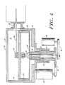
shaft 92 is concentrically mounted within theshaft 84 and journaled for rotation therein on a bearing and vacuum seal assembly generally designated 93. Any suitable rotary vacuum seal, such as a ferrofluidic rotary vacuum seal, may be employed. On end of theshaft 92 is connected to pivot bearing 94 to be described vacuum-mounted through theturntable 82, and the other end of theshaft 92 is operatively coupled to a R-drive motor 92 via a belt and wheel arrangement generally designated 98. As described more fully below, with the controlled rotation of the shaft of the R-drive motor 96, the wafer arm of both embodiments of the R, TT movable wafer arm assembly to be described is controllably translated in the R-direction for loading and unloading idividual wafers into and out of theplural reaction chambers 12 and queuingstation 14 through the associatedvacuum lock 20. - Referring now to Figures 2, 4, and 5, th
wafer arm assembly 80 includes a wafer receiving and releasing paddle assembly generally designated 100. Thepaddle assembly 100 includes aplatform 102 having a central opening generally designated 104 therethrough. Themember 102 terminated in laterally spacedfingers 106 having wafer-periphery engagingupstanding flanges 108 integrally formed on the free ends thereof. A releasable abutment generally designated 110 having abumper portion 112 and anintegral tail portion 114 is mounted for sliding motion to theplatform member 102. As best seen in Figure 8, a coil spring 116 is mounted between thereleasable abutment 110 and themember 102 which urges thebumper 112 in the direction of anarrow 118 so as to abut and therewith frictionally engage the periphery of a wafer, not shown, received between thebumper 112 and theflanges 108. Thetail 114 includes a downwardly dependingstop 120 to be described that is slidably received in an elongated aperture provided therfor in theplatform member 102 that is cooperative with an upstanding abutment to be described to release the frictional wafer engagement as the arm reaches its position of maximum extension. Thepaddle assembly 100 is mounted betweenplates 124 to a carriage assembly generally designated 126 that is slidable mounted onlinear bearings 128 that are fastened to endposts 130 upstanding from and fastened to therotatable turntable 82. - The
carriage 126 is controllably moved in either direction along thelinear bearings 128 for loading and unloading wafers individually to and from theseveral plasma reactors 12 and the queuingstation 18. Amember 131 is pivotally mounted subjacent thecarriage 126, which houses therein a linear bearing, not shown. Ashaft 132 is slidably received through the linear bearing of the pivotinghousing 131. One end of theshaft 132 is slidably mounted in asleeve 134 that is mounted for rotary motion to theturntable 82 via apivot bearing 136, and the other end of theshaft 132 is fastened to aneedle bearing assembly 138 that is pivotally fastened to a crankarm 140 mounted for rotation with theshaft 92 of the R-drive motor 96 (Figure 4) via a mountingcoupling 142 fastened to theturntable 82. - With controlled rotation of the Theta-
drive motor 88, theturntable 82 and therewith thepaddle assembly 100 is rotated to that TT coordinate that corresponds to any selected one of the angular locations of the plural plasma reaction chambers designated TT1 through TT4 in Figure 2, and to that TT coordinate that corresponds to the angular location of thewafer queuing station 14 designated TT5 in Figure 2. With the controlled rotation of the R-drive motor 96, thecrank 140 traces an arcuate path as illustrated by anarrow 144. Thearm 132 therewith pivots on the pivot bearing 136 as shown by anarrow 146, and moves thecarriage 126 linearly along thebearings 128 in a direction that corresponds to the sense of rotation of the X-drive motor as illustrated by anarrow 148. The arm is either more or less elongated relative to thecoupling 136 as it is pivoted by thecrank 140, and depending on the sense of the rotation, it slides within thesleeve 134 and within thehousing 131 as illustrated by anarrow 150. When thecrank 140 is turned to its maximum clockwise position, thepaddle assembly 100 moves into its fully retracted position as illustrated generally at 152 in Figure 6. With counterclockwise motion of thecrank arm 140 the paddle moves along the R direction as illustrated generally at 154 in Figure 7. As thepaddle assembly 100 nears its fully extended position, close to the maximum allowed counterclockwise rotation of the R-drive motor, thestop 120 on thetail portion 110 abuts the confronting wall of theupstanding end post 130, such that with continued motion of the paddle along the R direction thebumper 110 draws away from theflanges 108 and thereby releases the frictional engagement of the wafer periphery. In the maximum extended position, then, the wafers are free to be loaded or unloaded to and from any selectedplasma reactor 12 and/or are free for pick up or delivery back into the queuingstation 14. -
Contacts 156, preferably three in number, are mounted to theplatform member 102 of thepaddle assembly 100 as shown in Figure 7. The contacts are operative in response to the presence of a supported wafer to provide a three-point signal indicative of whether or not the wafer is properly seated on the wafer transfer arm. The contacts preferably are formed on a printed circuit board, not shown, mounted to thepaddle assembly 100. A different number thereof, or other sensing means may be utilized, so long as an accurate indication of intended seating of individual wafers is provided. - Referring now to Figure 9, generally designated at 160 is a partially pictorial and partially schematic side view illustrating a plasma reactor of the multiple-processing and contamination-free plasma etching system according to the present invention. Each of the plasma reactors 160 includes a
top plate 162, a spaced-apartbottom plate 164 and acylindrical sidewall 166 cooperate to define a plasma chamber generally designated 168. A first electrode generally designated 170 is fastened to thebottom plate 164. A pedestal schematically illustrated dashed at 172 is slidably mounted centrally in thebottom electrode 170 for vertical motion with the shaft of a pneumatic cylinder schematically illustrated in dashedoutline 174. As described more fully below, thepedestal 172 is cooperative with the paddle arm assembly to allow for removal and delivery of individual wafers into and out of the plasma chambers. The pedestalpneumatic cylinder 174 is driven by a controlled air supply, now shown, operatively coupled thereto via anair input port 176 and anair output port 178. As illustrated by dashedoutline 180, a source of colling liquid, not shown, is coupled to internal fluid flow passageways, not shown, provided through the interior of thebottom electrode 170 via input andoutput ports 182, 184 for removing the heat produced in the bottom electrode during plasma etching. A top electrode generally designated 186 is fastened to a support shaft generally designated 188 that is slidably received through thetop plate 162 in a vacuum-tight sealing engagement therewith as by a stainless steel vacuum bellows 190 fastened between thetop plate 162 and a superadjacentshaft support plate 187. Thetop electrode 186 includes internal cooling/heating fluid flow passageways schematically illustrated in dashedoutline 189 that are coupled via fluid flowsconduits 190 disposed in theshaft 188 to a source, not shown, via aliquid input port 194 and an output port 196 provided in theplate assembly 187. A pneumatic actuator generally designated 200 having aram 202 is mounted to thesupport plate assembly 187. With theram 202 in its extended position, not shown, theplate 187 moves upwardly, and therewith theshaft 188 andelectrode 186 move upwardly and away from the stationarybottom electrode 170. With the ram lowered as shown, micrometer adjustment posts 204 fastened to theplate assembly 187 bear against thetop plate 162 and therewith support thetop electrode 186 in an intended spaced-apart relation with thebottom electrode 170. The gap between the electrodes is adjustable by changing the length of the micrometer adjustment posts selectively. In the preferred embodiment, between 2/16 inch to 2 inches of gap adjustment is provided. - The
shaft 188 has a hollow interior generally designated 206, and alaser window 208 is mounted across the hollow of theshaft 206. The beam of an external laser, not shown, passes through the window and hollow shaft for providing end-point determinations of the plasma etch state. Other end-point determination means, such as a lateral optical detector, may be employed as well without departing from the inventive concept. Reactant gas injection ports 210 are coupled via internal shaft conduits provided therefor, not shown, to a liquid-cooled showerhead gas manifold illustrated in dashed outline 211 in theupper electrode 186. Reactant gas is controllably released therefrom into the plasma reactor, and radio frequency power is applied in the plasma reaction chambers. In an alternative embodiment, the spacing between the electrodes can be preselected for each particular plasma process, and additional micrometers, in place of thepneumatic actuators 200, can advantageously be employed. - Referring now to Figure 10, generally designated at 212 is a schematic diagram illustrating the presently preferred gas injection and controlled vacuum systems. Preferably, four independently valved sources of gases are respectively connected to individual ones of plasma vessels via corresponding ones of a plurality of gas manifolds, two banks of gas sources generally designated 214, 216 and two
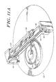
manifolds vacuum system 22 is operatively coupled in common to the plural plasma reactor chambers, to the queuingstations 224, and to the load and unloadisland 226. The vacuum system controls the vacuum condition in the entire system, so that the wafers are free from possible contamination as the vacuum locks are severally opened and closed during single and multiple phase processing wafer transfer. It should be noted that while four plasma reactors are disclosed, a greater or a lesser number can be employed without departing from the inventive concept. - Referring now to Figure 11A, generally designated at 230 is a perspective view of an alternative embodiment of the X. TT wafer arm assembly according to the present invention. The
assembly 230 includes apully 232 mounted for rotation with the shaft of the TT drive motor as best seen in Figure 11B. Thepulley 232 includes agrooved rim 234 around which acable 236 is wrapped. The cable is drawn tangentally to thegrooved rib 234 in opposing directions, and respectively wrapped overpulleys slide 242, as best seen at 244 in Figure 11B. With the angular rotation of thepulley 232, theslide 242 linearly moves along thelinear bearings 246. A wafer arm generally designated 248 is mounted for movement with theslide 242 such that thearm 248 is controllably extended and retracted in dependence on the angular position of thepulley 232. To provide constant-tension in thecable 236, the ends of the cable preferably are terminated in theslide 242 against resilient biasing elements generally designated 250 in Figure 12. Thecable 236 as it stretches is pulled in a reverse direction by theresilient couplings 250 for maintaining its intended state. - During the plasma chamber load cycles, the Theta-drive motor turns the turntable of the R, TT wafer arm assembly to the TT coordinate of the queuing station in either embodiment of the R, TT movable wafer arm assembly. The vacuum lock of the associated interface is released, and the arm is extended under the wafer in the addressed cassette slot position. The arm is then retracted back into the load and unload module, and the vacuum lock is restored. The R, TT wafer arm assembly is then rotated to the TT coordinate of the selected plasma reactor. The associated chamber door is then rotated to its open condition for providing access to the selected reaction chamber, and the upper electrode is raised. The wafer receiving arm is then extended in the R direction through the associated slot valve opening and into the selected reaction chamber. As it approaches the limit of its maximum radial travel, the depending stop flange on the wafer arm abuts the upstanding end post on the turntable and, with continued radial motion, the bumper withdraws thereby freeing the wafer from peripheral friction engagement. The central pedestal of the lower electrode is then controllably raised by its pneumatic actuator, and therewith the wafer supported on the arm is elevated upwardly off of the wafer support platform. Thereafter, the wafer arm is retracted out of the plasma chamber through the open slot valve and back into the load and unload station. The pedestal is then controllably lowered. The wafer lowers therewith until the pedestal is in its retracted position and the wafer is supported on the surface of the lower electrode. The associated chamber door is then closed, and the upper electrode is lowered to that precise preselected gap that implements the particular plasma process being run. The intended reactants are then injected through the gas manifold of the upper electrode, the radio frequency power is applied. Whereupon, plasma etching of each single wafer is continued until the laser provides a signal indication that the proper end-point has been achieved. Thereafter, the RF power is turned-off, the vacuum lock is opended, and the above-described process is repeated, but in reverse order, for removing the wafer out of that plasma chamber and back into the load and unload station. The wafer can then be moved into another plasma reactor for a subsequent process in a two or more step processing mode, or back into the cassette in a one-step processing mode.
- The load and unload module, queuing station, and plural reactors are operable in three basic modes, namely, where each reactor is simultaneously performing the same plasma reaction, where each plasma reactor is simultaneously performing two or more different plasma processes, and where the plasma reactors are severally being operated to provide multiple-step processing of single wafers before their return back to the queuing station. In each case, the wafers are transferred and processed in a controlled vacuum environment such that atmospheric exposure and handling induced contamination are wholly eliminated.
- Figure 13-17 are scanning electron micrographs illustrating exemplary microstructures capable of being formed in a single-step process, and Figure 18 is a scanning electron micrograph illustrating an exemplary microstructure capable of being fabricated in a double-step etch process. Figure 13 shows generally at 260 polysilicon with an overlayed
photoresist 262 on the surface of thesilicon dioxide layer 264 of the wafer. For exemplary low-resistivity (12-13 ohms) doped polysilicon, CCl₄ at 20 sccm and He at 30 sccm are applied to the plasma reactor at a pressure of 100 mt and a power of 300 watts. The etch occurs for approximately 1 1/2 minutes. As shown in Figure 14 dopedpolysilicon 265 having a comparatively high resistivity (30-200 ohms per sq.) and having a slopped profile mask is illustrated. For the illustrated microstructure, SF₆ at 50 sccm and freon 115 (C₂CIF₅) at 50 sccm are controllably injected into a plasma reactor at 150 mt pressure and a 100 watt power. After about 2 1/2 minutes, the illustrated doped polysilicon microstructure is fabricated. - Referring now to Figure 15, generally designated at 266 is a SEM illustrating an exemplary trench etc. The photoresist is removed, and a trench generally designated 268 is formed in the
silicon 272 by injecting BCl₃ at 5 sccm and Cl₂ at 25 sccm into the plasma reactor at a 100 mt chamber pressure and at 750 watts power for about 20 minutes. - Referring now to Figure 16, refractory silcide, TaSi/poly, is illustrated generalldy at 274. The
silicon dioxide surface 276 is overlayed with apolysilicon layer 278 upon which is overlayed the TaSi/poly 280 over which is the photoresist. The microstructure is fabricated by injecting CCl₄ at 20 sccm and He at 30 sccm into a plasma reactor maintained at a chamber pressure of 80 mt and a radio frequency power of 300 watts for about 3 1/2 minutes. - Referring now to Figure 17, generally designated 282 is another microstructure exemplary of the single-step structures capable of being fabricated by the contamination-free and multiple-processing plasma reactor of the present invention. As illustrated, a
photoresist 284 is layed over an aluminum andsilicon layer 286 which is overlayed via aTiW layer 288 on the wafer surface. The illustrated structure was fabricated by injecting BCl₃ at 50 sccm with Cl₂ at 15 sccm into the plasma reactor maintained at 125 mt chamber pressure and a 300 watt RF power for about 2 1/2 to 3 1/2 minutes. - Referring now to Figure 18, generally designated at 290 is a silicon dioxide/poly/silicon dioxide/poly sandwich structure illustrating an exemplary two-step process. A poly layer designated poly 1 and an oxide layer designed oxide are formed after etching with C₂F₆ at 100 sccm at a 700 mt pressure and a 600 watt radio frequency power in a first chamber. Thereafter, the
upper poly 2 layer and the oxide and an overlayed photoresist layer are formed by a separate step employing CCl₄ at 20 sccm and He at 30 sccm in a second reaction chamber maintained at a 100 militore chamber pressure and a 600 watt radio frequency power. - With respect now to Figs. 19-24, the processor control for wafer throughput is illustrated. In particular, Fig. 19 illustrates a state diagram for overall system operation. In the
state 300, system initialization procedures are accomplished which take the system from a turn-on state through necessary warm-ups and start up proceedures. Transition to asubsequent state 302 occurs once the system initialization has been completed.State 302 exists until a cassette has been placed into the cassette queue station and all door interlock switches are activated. The transition from the determineready state 302 to amachine initialization state 304 occurs once these conditions have been met and the operator initiates system operation through a start button, provided no other system interrupt signals or hold designations have occurred and provided the user has not activated the diagnostic state 306 which is alternatively entered from the determineready state 302. - The diagnostic state 306 runs a set of diagnostics on the system should that state be entered by the user. Otherwise, the
machine initialization state 304 accomplishes a final set of system power-ons, gas perge or other initialization steps which would not normally be entered in thesystem initialization state 300 for time and/or power considerations. - From the machine initialization state 304 a standby state 306 may be entered by operator designation through a standby button which effectively aborts the processing steps back to the determine
ready state 302. Otherwise, from themachine initialization state 304, once the initialization functions have been completed, the system transitions to a cassette pump downstate 310 in which a vacuum is drawn from thewafer queuing station 14 placing it into the environment of the transport arm and plural etch vessels. After pump down of thewafer queuing station 14,state 310 processing will normally transition to thestate 312 in which the wafers and the cassette at the queuingstation 14 are processed in sequence as illustrated in the subsequent figures. Alternatively, if in the determineready state 302 the operator had activated a clear wafer instruction, processing would transition to aclear wafer state 314 in which, in liew of cassette processing, wafers are cleared from the system. In the case of eachstate ready state 302. - If the
cassette processing state 312 is entered, the system processes each wafer in the cassette according to a wafer command list entered into the system and described below. Once that cycle is complete, processing proceeds to astate 316 which vents thewafer queuing station 14 and waits until removal of the cassette at which point the system transitions tostate 300. - Should any error occur in normal system operation, as determined by processor error detection, processing from each of the states of Fig. 19 will return to the
system initialization state 300 to rerun the power-on initialization functions. - The operation within the
cassette process state 312 follows a flexible processes control illustrated in the flow diagram of Figure 20. As illustrated there processing proceeds betweenstate 320 labeled slots,state 322 labeled wafers,state 324 labeled wafer commands, andstate 326 labeled machine monitors. The processing of Figure 20 is initiated when thestate 312 is entered with a cassette of unprocessed wafers, and starts, and finishes, instate 320.State 320 initiates a wafer start command for each slot containing an unprocessed wafer using, for example, a top to bottom priority scheme, or any other priority scheme which may be programmed. From thestate 320 for a selected slot, and corresponding wafer, processing proceeds to thewafer state 322. Fromstate 322 the processing commands or specifications for each wafer are accessed in asubsequent state 324, wafer commands. The wafer commands will be programmed into the system corresponding to the desired processing of each wafer, for example, one or more etches for a designated time period or depth in a designated gas. The commands in thestate 324 are executed in sequence, and each command commences a set of machine control operations which occur instate 326, machine monitors. - At the completion of each wafer command, representing for example, a single etch cycle for a wafer as described below, processing returns to the
wafer command state 324 to execute another wafer command. After all wafer commands have been executed for a particular wafer, processing returns to thestate 322 and from thence tostate 320 thereby sequencing through the wafers and the cassette slots. - Processing within the
machine control state 326 is in accordance with the wafer transport algorithms of Figs. 21, 22 and 23 and the internal chamber or vessel processing algorithm of Fig. 24. In each case where processing halts for receipt of system instructions to proceed, processor state evaluation checks for existence conditions necessary for the unit to proceed to the next step. - With particular regard to Fig. 21 illustrates processing for moving a wafer from one chamber or vessel to another, in accordance with wafer commands specifying multiple chamber or vessel processing. As shown there processing commences at
initialization state 330.Subsequent state 332 directs the transport arm wafer support table from one chamber or vessel to the desired chamber or vessel wherein the wafer to be moved is located. Once that positioning is accomplished asubsequent state 334 activates the valve and arm mechanisms in a transition to astate 336. Instate 336 the system repositions the transport arm wafer support table to the destination chamber or vessel and transitions to astate 338 which, when it receives control signals, activates the arm mechanism and valving on the applicable chamber to place the wafer in that particular chamber in the transition to astate 340. Whenstate 340 is reached, the wafer relocation function is complete and processing returns to the next wafer command instate 324. - Fig. 22 illustrates the processing wherein a wafer is moved from a chamber or etch vessel to a slot of the cassette. From an
initialization state 350 processing transitions to astate 352 which awaits the direction of the transport arm wafer support table to the desired chamber having the wafer to be returned to the cassette. Once the proper positioning is accomplished, the transition fromstate 352 tostate 354 sends a request to the command list asking to be instructed to remove the wafer from the chamber. When that instruction is received instate 354, the transition tostate 356 executes the machine instruction to open the valves and move the transport arm to pick up the wafer in the chamber and extract it from the chamber or vessel and in addition to request from the wafer command list the instructions to move to the cassette. When those instructions are executed and the arm is positioned to apply a wafer to the cassette, the system transitions tostate 358 and sends a request to the wafer processing list for instructions to place the wafer into the cassette and identified slot. When that information is received the transition to the donestate 360 executes the wafer insertion into the cassettes slot and returns processing back to the algorithm of Fig. 20. - Fig. 23 illustrates the algorithm for transferring a wafer from the cassette to a designated chamber in accordance with instructions in the wafer command list. From an
initialize state 370, processing transitions to astate 372 in which the request is sent to the command list for instructions to position the arm to the cassette and such arm manipulation is executed. When the arm is appropriately positioned instate 372, the system transitions tostate 374 in which a request for the instructions to extract a wafer from the cassette is sent. Thestate 374 has two possible outcomes, in the first represented bybranch 376, a wafer is not found in the slot in which the system has been instructed to retrieve it by the transport arm. In this case the system transitions to a donestate 378 indicating that the algorithm of Fig. 23 has progressed as far as it can, albeit in an abort condition. In the other possible outcome ofstate 374, the wafer is found and the system transitions fromstate 374 tostate 380 in which instructions are received from the wafer processing list to position the transport arm support table at the destination chamber or vessel. When, instate 380, that destination chamber is reached, the system transitions to astate 382 in which the system requests and receives instructions from the command list (if the chamber is ready) to insert that wafer into the chamber. In the transition fromstate 382 to the completedstate 378, the mechanisms of the arm and the chamber valving are activated in order to install the wafer into the chamber. - Fig. 24 illustrates the processing of the system for accomplishing wafer etching within a chamber to which the system has allocated a wafer from the cassette at the queuing station.
- The processing of Fig. 24 is initiated by a start command obtained from the command list which initiates a
state 390. Thestate 390 loops through anerror recognition state 392 to a startcommand wait step 394 if the start command is determined to have incorrect signature. Otherwise, processing from astate 390 proceeds to astate 392 in which the valve to the chamber is sealed and the electrode spacing set to the etch condition. Asubsequent step 394 waits for confirmation signals from microswitches indicating proper gate closure and electrode positioning. Subsequently astate 396 commences the flow of a gas, selected from the wafer command list, for the desired processing and waits for a steady state gas condition, based on time or other factors, to occur. Subsequently a transition to astate 398 activates the RF plasma generation between the electrodes used for plasma etching within the gas and wafer processing by gas vapor etch continues until a parameter indicating complete processing is obtained. Such a parameter may be a function of time, detected etch depth, or other factors. Once wafer processing is indicated as complete, the transition fromstate 398 tostate 400 deactivates the RF and instate 400 the gas environment in the chamber is evacuated so that, insubsequent state 402, the electrodes can be respaced for wafer removal, and the gate or chamber doors opened to the environment of the transport arm without fear of leaking reactor gas into that environment.State 402 transitions tostate 404 in which the system awaits confirmation by microswitch activation of proper electrode spacing and opening and transitions tostate 394 in which system processing returns to the flexible process control of Fig. 20.
Claims (12)
Priority Applications (1)
| Application Number | Priority Date | Filing Date | Title |
|---|---|---|---|
| EP95111001A EP0680074A3 (en) | 1986-10-24 | 1987-10-22 | Quad processor |
Applications Claiming Priority (2)
| Application Number | Priority Date | Filing Date | Title |
|---|---|---|---|
| US06/923,125 US4715921A (en) | 1986-10-24 | 1986-10-24 | Quad processor |
| US923125 | 1986-10-24 |
Related Child Applications (2)
| Application Number | Title | Priority Date | Filing Date |
|---|---|---|---|
| EP95111001.4 Division-Into | 1987-10-22 | ||
| EP95111001A Division EP0680074A3 (en) | 1986-10-24 | 1987-10-22 | Quad processor |
Publications (3)
| Publication Number | Publication Date |
|---|---|
| EP0264945A2 true EP0264945A2 (en) | 1988-04-27 |
| EP0264945A3 EP0264945A3 (en) | 1989-09-13 |
| EP0264945B1 EP0264945B1 (en) | 1996-03-13 |
Family
ID=25448159
Family Applications (2)
| Application Number | Title | Priority Date | Filing Date |
|---|---|---|---|
| EP87115508A Revoked EP0264945B1 (en) | 1986-10-24 | 1987-10-22 | Multichamber plasma etching system |
| EP95111001A Withdrawn EP0680074A3 (en) | 1986-10-24 | 1987-10-22 | Quad processor |
Family Applications After (1)
| Application Number | Title | Priority Date | Filing Date |
|---|---|---|---|
| EP95111001A Withdrawn EP0680074A3 (en) | 1986-10-24 | 1987-10-22 | Quad processor |
Country Status (6)
| Country | Link |
|---|---|
| US (1) | US4715921A (en) |
| EP (2) | EP0264945B1 (en) |
| JP (1) | JPS63133532A (en) |
| KR (1) | KR880005675A (en) |
| CA (1) | CA1283174C (en) |
| DE (1) | DE3751738T2 (en) |
Cited By (5)
| Publication number | Priority date | Publication date | Assignee | Title |
|---|---|---|---|---|
| EP0272141A2 (en) * | 1986-12-19 | 1988-06-22 | Applied Materials, Inc. | Multiple chamber integrated process system |
| EP0343530A2 (en) * | 1988-05-24 | 1989-11-29 | Balzers Aktiengesellschaft | Vacuum installation |
| EP0416646A2 (en) * | 1989-09-08 | 1991-03-13 | Tokyo Electron Limited | Apparatus and method for processing substrates |
| US5882165A (en) * | 1986-12-19 | 1999-03-16 | Applied Materials, Inc. | Multiple chamber integrated process system |
| GB2359416A (en) * | 1999-09-07 | 2001-08-22 | Bosch Gmbh Robert | Etching unit for HF vapour etching of substrates |
Families Citing this family (108)
| Publication number | Priority date | Publication date | Assignee | Title |
|---|---|---|---|---|
| US6214119B1 (en) | 1986-04-18 | 2001-04-10 | Applied Materials, Inc. | Vacuum substrate processing system having multiple processing chambers and a central load/unload chamber |
| US5102495A (en) * | 1986-04-18 | 1992-04-07 | General Signal Corporation | Method providing multiple-processing of substrates |
| US5013385A (en) * | 1986-04-18 | 1991-05-07 | General Signal Corporation | Quad processor |
| US5308431A (en) * | 1986-04-18 | 1994-05-03 | General Signal Corporation | System providing multiple processing of substrates |
| CA1331163C (en) * | 1986-04-18 | 1994-08-02 | Applied Materials, Inc. | Multiple-processing and contamination-free plasma etching system |
| US6103055A (en) * | 1986-04-18 | 2000-08-15 | Applied Materials, Inc. | System for processing substrates |
| US5292393A (en) * | 1986-12-19 | 1994-03-08 | Applied Materials, Inc. | Multichamber integrated process system |
| US4951601A (en) * | 1986-12-19 | 1990-08-28 | Applied Materials, Inc. | Multi-chamber integrated process system |
| JPS63204726A (en) * | 1987-02-20 | 1988-08-24 | Anelva Corp | Vacuum treatment device |
| US4906328A (en) * | 1987-07-16 | 1990-03-06 | Texas Instruments Incorporated | Method for wafer treating |
| US5435682A (en) * | 1987-10-15 | 1995-07-25 | Advanced Semiconductor Materials America, Inc. | Chemical vapor desposition system |
| US5906688A (en) * | 1989-01-11 | 1999-05-25 | Ohmi; Tadahiro | Method of forming a passivation film |
| US5591267A (en) * | 1988-01-11 | 1997-01-07 | Ohmi; Tadahiro | Reduced pressure device |
| US5019233A (en) * | 1988-10-31 | 1991-05-28 | Eaton Corporation | Sputtering system |
| US5683072A (en) * | 1988-11-01 | 1997-11-04 | Tadahiro Ohmi | Thin film forming equipment |
| US5076205A (en) * | 1989-01-06 | 1991-12-31 | General Signal Corporation | Modular vapor processor system |
| US5186718A (en) * | 1989-05-19 | 1993-02-16 | Applied Materials, Inc. | Staged-vacuum wafer processing system and method |
| DE69120446T2 (en) * | 1990-02-19 | 1996-11-14 | Canon Kk | Process for producing deposited metal layer containing aluminum as the main component using alkyl aluminum hydride |
| US5100502A (en) * | 1990-03-19 | 1992-03-31 | Applied Materials, Inc. | Semiconductor wafer transfer in processing systems |
| US5186594A (en) * | 1990-04-19 | 1993-02-16 | Applied Materials, Inc. | Dual cassette load lock |
| US5213996A (en) * | 1990-07-04 | 1993-05-25 | Mitsubishi Denki Kabushiki Kaisha | Method and apparatus for forming interconnection pattern and semiconductor device having such interconnection pattern |
| JP2528026B2 (en) * | 1990-07-04 | 1996-08-28 | 三菱電機株式会社 | Wiring pattern forming method and apparatus |
| US5286296A (en) * | 1991-01-10 | 1994-02-15 | Sony Corporation | Multi-chamber wafer process equipment having plural, physically communicating transfer means |
| JPH0766919B2 (en) * | 1991-02-20 | 1995-07-19 | 株式会社半導体プロセス研究所 | Semiconductor manufacturing equipment |
| US5171393A (en) * | 1991-07-29 | 1992-12-15 | Moffat William A | Wafer processing apparatus |
| JP2598353B2 (en) * | 1991-12-04 | 1997-04-09 | アネルバ株式会社 | Substrate processing device, substrate transfer device, and substrate replacement method |
| JP2751975B2 (en) * | 1991-12-20 | 1998-05-18 | 株式会社日立製作所 | Load lock chamber of semiconductor processing equipment |
| JP3030160B2 (en) * | 1992-04-28 | 2000-04-10 | 東京エレクトロン株式会社 | Vacuum processing equipment |
| US5404894A (en) * | 1992-05-20 | 1995-04-11 | Tokyo Electron Kabushiki Kaisha | Conveyor apparatus |
| US5534072A (en) * | 1992-06-24 | 1996-07-09 | Anelva Corporation | Integrated module multi-chamber CVD processing system and its method for processing subtrates |
| US5248371A (en) * | 1992-08-13 | 1993-09-28 | General Signal Corporation | Hollow-anode glow discharge apparatus |
| JPH0828333B2 (en) * | 1992-11-30 | 1996-03-21 | 株式会社半導体プロセス研究所 | Semiconductor device manufacturing equipment |
| JPH0828334B2 (en) * | 1992-11-30 | 1996-03-21 | 株式会社半導体プロセス研究所 | Semiconductor device manufacturing apparatus and method of using the same |
| US5647945A (en) * | 1993-08-25 | 1997-07-15 | Tokyo Electron Limited | Vacuum processing apparatus |
| US5588827A (en) * | 1993-12-17 | 1996-12-31 | Brooks Automation Inc. | Passive gas substrate thermal conditioning apparatus and method |
| US6245189B1 (en) * | 1994-12-05 | 2001-06-12 | Nordson Corporation | High Throughput plasma treatment system |
| GB9425349D0 (en) * | 1994-12-15 | 1995-02-15 | Oxford Plasma Technology Ltd | Substrate loading apparatus |
| US6193506B1 (en) | 1995-05-24 | 2001-02-27 | Brooks Automation, Inc. | Apparatus and method for batch thermal conditioning of substrates |
| US5588789A (en) * | 1995-07-06 | 1996-12-31 | Brooks Automation | Load arm for load lock |
| US5664925A (en) * | 1995-07-06 | 1997-09-09 | Brooks Automation, Inc. | Batchloader for load lock |
| US5609459A (en) * | 1995-07-06 | 1997-03-11 | Brooks Automation, Inc. | Door drive mechanisms for substrate carrier and load lock |
| US5613821A (en) * | 1995-07-06 | 1997-03-25 | Brooks Automation, Inc. | Cluster tool batchloader of substrate carrier |
| US5607276A (en) * | 1995-07-06 | 1997-03-04 | Brooks Automation, Inc. | Batchloader for substrate carrier on load lock |
| JPH0936198A (en) * | 1995-07-19 | 1997-02-07 | Hitachi Ltd | Vacuum processor and semiconductor production line using the processor |
| US6672819B1 (en) | 1995-07-19 | 2004-01-06 | Hitachi, Ltd. | Vacuum processing apparatus and semiconductor manufacturing line using the same |
| US5746565A (en) * | 1996-01-22 | 1998-05-05 | Integrated Solutions, Inc. | Robotic wafer handler |
| US5863170A (en) * | 1996-04-16 | 1999-01-26 | Gasonics International | Modular process system |
| US5667592A (en) * | 1996-04-16 | 1997-09-16 | Gasonics International | Process chamber sleeve with ring seals for isolating individual process modules in a common cluster |
| US5855465A (en) * | 1996-04-16 | 1999-01-05 | Gasonics International | Semiconductor wafer processing carousel |
| US5746434A (en) * | 1996-07-09 | 1998-05-05 | Lam Research Corporation | Chamber interfacing O-rings and method for implementing same |
| US6714832B1 (en) * | 1996-09-11 | 2004-03-30 | Hitachi, Ltd. | Operating method of vacuum processing system and vacuum processing system |
| US5928389A (en) * | 1996-10-21 | 1999-07-27 | Applied Materials, Inc. | Method and apparatus for priority based scheduling of wafer processing within a multiple chamber semiconductor wafer processing tool |
| JP3393035B2 (en) | 1997-05-06 | 2003-04-07 | 東京エレクトロン株式会社 | Control device and semiconductor manufacturing device |
| US5944857A (en) * | 1997-05-08 | 1999-08-31 | Tokyo Electron Limited | Multiple single-wafer loadlock wafer processing apparatus and loading and unloading method therefor |
| US5894760A (en) * | 1997-06-12 | 1999-04-20 | Brooks Automation, Inc. | Substrate transport drive system |
| US5911896A (en) * | 1997-06-25 | 1999-06-15 | Brooks Automation, Inc. | Substrate heating apparatus with glass-ceramic panels and thin film ribbon heater element |
| US6054688A (en) * | 1997-06-25 | 2000-04-25 | Brooks Automation, Inc. | Hybrid heater with ceramic foil serrated plate and gas assist |
| US6123502A (en) * | 1997-07-08 | 2000-09-26 | Brooks Automation, Inc. | Substrate holder having vacuum holding and gravity holding |
| US6312525B1 (en) | 1997-07-11 | 2001-11-06 | Applied Materials, Inc. | Modular architecture for semiconductor wafer fabrication equipment |
| US6139245A (en) * | 1997-07-11 | 2000-10-31 | Brooks Automation Inc. | Robot arm relocation system |
| US6002840A (en) * | 1997-09-30 | 1999-12-14 | Brooks Automation Inc. | Substrate transport apparatus |
| JP3582330B2 (en) * | 1997-11-14 | 2004-10-27 | 東京エレクトロン株式会社 | Processing apparatus and processing system using the same |
| US7253109B2 (en) | 1997-11-26 | 2007-08-07 | Applied Materials, Inc. | Method of depositing a tantalum nitride/tantalum diffusion barrier layer system |
| WO1999027579A1 (en) * | 1997-11-26 | 1999-06-03 | Applied Materials, Inc. | Damage-free sculptured coating deposition |
| US6072898A (en) | 1998-01-16 | 2000-06-06 | Beaty; Elwin M. | Method and apparatus for three dimensional inspection of electronic components |
| US6067596A (en) * | 1998-09-15 | 2000-05-23 | Compaq Computer Corporation | Flexible placement of GTL end points using double termination points |
| US6960057B1 (en) | 1998-09-30 | 2005-11-01 | Brooks Automation, Inc. | Substrate transport apparatus |
| US6328858B1 (en) | 1998-10-01 | 2001-12-11 | Nexx Systems Packaging, Llc | Multi-layer sputter deposition apparatus |
| US6217272B1 (en) | 1998-10-01 | 2001-04-17 | Applied Science And Technology, Inc. | In-line sputter deposition system |
| US6485250B2 (en) | 1998-12-30 | 2002-11-26 | Brooks Automation Inc. | Substrate transport apparatus with multiple arms on a common axis of rotation |
| US6120229A (en) * | 1999-02-01 | 2000-09-19 | Brooks Automation Inc. | Substrate carrier as batchloader |
| US6267545B1 (en) | 1999-03-29 | 2001-07-31 | Lam Research Corporation | Semiconductor processing platform architecture having processing module isolation capabilities |
| US6095741A (en) * | 1999-03-29 | 2000-08-01 | Lam Research Corporation | Dual sided slot valve and method for implementing the same |
| US6440261B1 (en) | 1999-05-25 | 2002-08-27 | Applied Materials, Inc. | Dual buffer chamber cluster tool for semiconductor wafer processing |
| US6244811B1 (en) | 1999-06-29 | 2001-06-12 | Lam Research Corporation | Atmospheric wafer transfer module with nest for wafer transport robot |
| JP2001093791A (en) | 1999-09-20 | 2001-04-06 | Hitachi Ltd | Operation of vacuum treatment equipment and method for processing wafer |
| JP2001127044A (en) | 1999-10-29 | 2001-05-11 | Hitachi Ltd | Vacuum processor, and vacuum processing system |
| US6265803B1 (en) * | 1999-11-10 | 2001-07-24 | Brooks Automation, Inc. | Unlimited rotation vacuum isolation wire feedthrough |
| US6558509B2 (en) * | 1999-11-30 | 2003-05-06 | Applied Materials, Inc. | Dual wafer load lock |
| US6390448B1 (en) | 2000-03-30 | 2002-05-21 | Lam Research Corporation | Single shaft dual cradle vacuum slot valve |
| US6913243B1 (en) * | 2000-03-30 | 2005-07-05 | Lam Research Corporation | Unitary slot valve actuator with dual valves |
| US6530733B2 (en) | 2000-07-27 | 2003-03-11 | Nexx Systems Packaging, Llc | Substrate processing pallet and related substrate processing method and machine |
| US6821912B2 (en) | 2000-07-27 | 2004-11-23 | Nexx Systems Packaging, Llc | Substrate processing pallet and related substrate processing method and machine |
| US6682288B2 (en) | 2000-07-27 | 2004-01-27 | Nexx Systems Packaging, Llc | Substrate processing pallet and related substrate processing method and machine |
| DE60026476D1 (en) * | 2000-12-21 | 2006-05-04 | Oxford Instr Plasma Technology | Substrateneinschleusenvorrichtung |
| EP1220596A1 (en) | 2000-12-29 | 2002-07-03 | Icos Vision Systems N.V. | A method and an apparatus for measuring positions of contact elements of an electronic component |
| DE60137306D1 (en) * | 2001-03-02 | 2009-02-26 | Icos Vision Systems Nv | Self-supporting and adaptable measuring device |
| JP4364634B2 (en) | 2001-07-13 | 2009-11-18 | ブルックス オートメーション インコーポレイテッド | Trajectory planning and movement control strategy of two-dimensional three-degree-of-freedom robot arm |
| US7578649B2 (en) | 2002-05-29 | 2009-08-25 | Brooks Automation, Inc. | Dual arm substrate transport apparatus |
| US7100954B2 (en) | 2003-07-11 | 2006-09-05 | Nexx Systems, Inc. | Ultra-thin wafer handling system |
| US20060024451A1 (en) * | 2004-07-30 | 2006-02-02 | Applied Materials Inc. | Enhanced magnetic shielding for plasma-based semiconductor processing tool |
| US20070196011A1 (en) * | 2004-11-22 | 2007-08-23 | Cox Damon K | Integrated vacuum metrology for cluster tool |
| US20070134821A1 (en) * | 2004-11-22 | 2007-06-14 | Randhir Thakur | Cluster tool for advanced front-end processing |
| US20060240680A1 (en) * | 2005-04-25 | 2006-10-26 | Applied Materials, Inc. | Substrate processing platform allowing processing in different ambients |
| US9248568B2 (en) | 2005-07-11 | 2016-02-02 | Brooks Automation, Inc. | Unequal link SCARA arm |
| US7738987B2 (en) * | 2006-11-28 | 2010-06-15 | Tokyo Electron Limited | Device and method for controlling substrate processing apparatus |
| US10541157B2 (en) | 2007-05-18 | 2020-01-21 | Brooks Automation, Inc. | Load lock fast pump vent |
| KR101522324B1 (en) | 2007-05-18 | 2015-05-21 | 브룩스 오토메이션 인코퍼레이티드 | Load lock fast pump vent |
| JP2008109134A (en) * | 2007-10-17 | 2008-05-08 | Hitachi Ltd | Vacuum processing device and method of vacuum processing |
| US8834969B2 (en) * | 2007-10-24 | 2014-09-16 | Oerlikon Advanced Technologies Ag | Method for manufacturing workpieces and apparatus |
| JP5107961B2 (en) * | 2009-04-22 | 2012-12-26 | 株式会社日立製作所 | Vacuum processing apparatus and vacuum processing method |
| JP5698043B2 (en) * | 2010-08-04 | 2015-04-08 | 株式会社ニューフレアテクノロジー | Semiconductor manufacturing equipment |
| US9202733B2 (en) | 2011-11-07 | 2015-12-01 | Persimmon Technologies Corporation | Robot system with independent arms |
| US9401296B2 (en) | 2011-11-29 | 2016-07-26 | Persimmon Technologies Corporation | Vacuum robot adapted to grip and transport a substrate and method thereof with passive bias |
| JP5314789B2 (en) * | 2012-06-13 | 2013-10-16 | 株式会社日立製作所 | Vacuum processing apparatus and vacuum processing method |
| US9018108B2 (en) | 2013-01-25 | 2015-04-28 | Applied Materials, Inc. | Low shrinkage dielectric films |
| US20150041062A1 (en) * | 2013-08-12 | 2015-02-12 | Lam Research Corporation | Plasma processing chamber with removable body |
| US9970098B2 (en) * | 2013-12-16 | 2018-05-15 | United Technologies Corporation | Movable evaporation source |
Citations (4)
| Publication number | Priority date | Publication date | Assignee | Title |
|---|---|---|---|---|
| US4477311A (en) * | 1982-12-28 | 1984-10-16 | Fujitsu Limited | Process and apparatus for fabricating a semiconductor device |
| US4547247A (en) * | 1984-03-09 | 1985-10-15 | Tegal Corporation | Plasma reactor chuck assembly |
| US4592306A (en) * | 1983-12-05 | 1986-06-03 | Pilkington Brothers P.L.C. | Apparatus for the deposition of multi-layer coatings |
| EP0246453A2 (en) * | 1986-04-18 | 1987-11-25 | General Signal Corporation | Novel multiple-processing and contamination-free plasma etching system |
Family Cites Families (6)
| Publication number | Priority date | Publication date | Assignee | Title |
|---|---|---|---|---|
| JPS55141570A (en) * | 1979-04-18 | 1980-11-05 | Anelva Corp | Dry etching apparatus |
| JPS57149748A (en) * | 1981-03-12 | 1982-09-16 | Anelva Corp | Treating device for substrate |
| JPS6037129A (en) * | 1983-08-10 | 1985-02-26 | Hitachi Ltd | Equipment for manufacturing semiconductor |
| US4584045A (en) * | 1984-02-21 | 1986-04-22 | Plasma-Therm, Inc. | Apparatus for conveying a semiconductor wafer |
| US4548699A (en) * | 1984-05-17 | 1985-10-22 | Varian Associates, Inc. | Transfer plate rotation system |
| DE3788973T2 (en) * | 1986-04-04 | 1994-08-11 | Materials Research Corp | Method and device for handling and treating disc-like materials. |
-
1986
- 1986-10-24 US US06/923,125 patent/US4715921A/en not_active Expired - Lifetime
-
1987
- 1987-10-05 CA CA000548598A patent/CA1283174C/en not_active Expired - Lifetime
- 1987-10-22 EP EP87115508A patent/EP0264945B1/en not_active Revoked
- 1987-10-22 DE DE3751738T patent/DE3751738T2/en not_active Revoked
- 1987-10-22 EP EP95111001A patent/EP0680074A3/en not_active Withdrawn
- 1987-10-23 JP JP62268021A patent/JPS63133532A/en active Pending
- 1987-10-23 KR KR870011816A patent/KR880005675A/en not_active Application Discontinuation
Patent Citations (4)
| Publication number | Priority date | Publication date | Assignee | Title |
|---|---|---|---|---|
| US4477311A (en) * | 1982-12-28 | 1984-10-16 | Fujitsu Limited | Process and apparatus for fabricating a semiconductor device |
| US4592306A (en) * | 1983-12-05 | 1986-06-03 | Pilkington Brothers P.L.C. | Apparatus for the deposition of multi-layer coatings |
| US4547247A (en) * | 1984-03-09 | 1985-10-15 | Tegal Corporation | Plasma reactor chuck assembly |
| EP0246453A2 (en) * | 1986-04-18 | 1987-11-25 | General Signal Corporation | Novel multiple-processing and contamination-free plasma etching system |
Non-Patent Citations (2)
| Title |
|---|
| JOURNAL OF APPLIED PHYSICS. vol. 58, no. 6, 15 September 1985, NEW YORK US pages 2416 BY MICROWAVE DISCHARGE.- 2419* page 2416, paragraphs 1 - 3 * M.M.MOSLEHI: "LOW-TEMPERATURE DIRECT NITRIDATION OF SILICON IN NITROGEN PLASMA GENERATED BY MICROWAVE DISCHARGE" * |
| SEMICONDUCTOR INTERNATIONAL, October 1985, p. 52 * |
Cited By (10)
| Publication number | Priority date | Publication date | Assignee | Title |
|---|---|---|---|---|
| EP0272141A2 (en) * | 1986-12-19 | 1988-06-22 | Applied Materials, Inc. | Multiple chamber integrated process system |
| EP0272141B1 (en) * | 1986-12-19 | 1994-03-02 | Applied Materials, Inc. | Multiple chamber integrated process system |
| US5882165A (en) * | 1986-12-19 | 1999-03-16 | Applied Materials, Inc. | Multiple chamber integrated process system |
| EP0343530A2 (en) * | 1988-05-24 | 1989-11-29 | Balzers Aktiengesellschaft | Vacuum installation |
| EP0343530A3 (en) * | 1988-05-24 | 1990-12-27 | Balzers Aktiengesellschaft | Vacuum installation |
| EP0416646A2 (en) * | 1989-09-08 | 1991-03-13 | Tokyo Electron Limited | Apparatus and method for processing substrates |
| EP0416646A3 (en) * | 1989-09-08 | 1991-08-28 | Tokyo Electron Limited | Apparatus and method for processing substrates |
| US5164034A (en) * | 1989-09-08 | 1992-11-17 | Tokyo Electron Limited | Apparatus and method for processing substrate |
| GB2359416A (en) * | 1999-09-07 | 2001-08-22 | Bosch Gmbh Robert | Etching unit for HF vapour etching of substrates |
| GB2359416B (en) * | 1999-09-07 | 2002-06-26 | Bosch Gmbh Robert | Etching unit for hf vapour etching |
Also Published As
| Publication number | Publication date |
|---|---|
| KR880005675A (en) | 1988-06-30 |
| DE3751738D1 (en) | 1996-04-18 |
| US4715921A (en) | 1987-12-29 |
| CA1283174C (en) | 1991-04-16 |
| EP0680074A3 (en) | 1995-11-15 |
| EP0680074A2 (en) | 1995-11-02 |
| EP0264945A3 (en) | 1989-09-13 |
| JPS63133532A (en) | 1988-06-06 |
| EP0264945B1 (en) | 1996-03-13 |
| DE3751738T2 (en) | 1996-11-07 |
Similar Documents
| Publication | Publication Date | Title |
|---|---|---|
| US4715921A (en) | Quad processor | |
| US5013385A (en) | Quad processor | |
| US5308431A (en) | System providing multiple processing of substrates | |
| US5344542A (en) | Multiple-processing and contamination-free plasma etching system | |
| US6103055A (en) | System for processing substrates | |
| US5102495A (en) | Method providing multiple-processing of substrates | |
| US6776846B2 (en) | Integrated processing system having multiple reactors connected to a central chamber | |
| USRE43023E1 (en) | Dual loading port semiconductor processing equipment | |
| US5900105A (en) | Wafer transfer system and method of using the same | |
| US5944940A (en) | Wafer transfer system and method of using the same | |
| EP1195795B1 (en) | Vacuum apparatus and method | |
| US20020112368A1 (en) | Substrate cooling system | |
| US6429139B1 (en) | Serial wafer handling mechanism | |
| WO2000033355A2 (en) | Apparatus for storing and moving a cassette | |
| US6347919B1 (en) | Wafer processing chamber having separable upper and lower halves | |
| WO1999026796A1 (en) | Plasma processing methods and apparatus | |
| US6224680B1 (en) | Wafer transfer system | |
| KR101457342B1 (en) | Workpiece rotation apparatus for a plasma reactor system | |
| JP3549674B2 (en) | Substrate processing equipment with load lock chamber | |
| WO1999052143A1 (en) | Alignment processing mechanism and semiconductor processing device using it | |
| KR20080059068A (en) | Vertical heat processing apparatus and vertical heat processing method | |
| JPS6350433B2 (en) | ||
| US20230038276A1 (en) | Transfer device, processing system, and transfer method | |
| KR20240041559A (en) | Wafer transfer apparatus and wafe loading jig provided therein, and wafer transfer method by the apparatus | |
| JPS623581B2 (en) |
Legal Events
| Date | Code | Title | Description |
|---|---|---|---|
| PUAI | Public reference made under article 153(3) epc to a published international application that has entered the european phase |
Free format text: ORIGINAL CODE: 0009012 |
|
| AK | Designated contracting states |
Kind code of ref document: A2 Designated state(s): CH DE FR GB LI |
|
| PUAL | Search report despatched |
Free format text: ORIGINAL CODE: 0009013 |
|
| AK | Designated contracting states |
Kind code of ref document: A3 Designated state(s): CH DE FR GB LI |
|
| 17P | Request for examination filed |
Effective date: 19900309 |
|
| 17Q | First examination report despatched |
Effective date: 19911017 |
|
| GRAA | (expected) grant |
Free format text: ORIGINAL CODE: 0009210 |
|
| AK | Designated contracting states |
Kind code of ref document: B1 Designated state(s): CH DE FR GB LI |
|
| XX | Miscellaneous (additional remarks) |
Free format text: TEILANMELDUNG 95111001.4 EINGEREICHT AM 22/10/87. |
|
| REG | Reference to a national code |
Ref country code: CH Ref legal event code: NV Representative=s name: A. BRAUN, BRAUN, HERITIER, ESCHMANN AG PATENTANWAE |
|
| REF | Corresponds to: |
Ref document number: 3751738 Country of ref document: DE Date of ref document: 19960418 |
|
| ET | Fr: translation filed | ||
| PGFP | Annual fee paid to national office [announced via postgrant information from national office to epo] |
Ref country code: CH Payment date: 19960917 Year of fee payment: 10 |
|
| PGFP | Annual fee paid to national office [announced via postgrant information from national office to epo] |
Ref country code: GB Payment date: 19960926 Year of fee payment: 10 Ref country code: FR Payment date: 19960926 Year of fee payment: 10 |
|
| PGFP | Annual fee paid to national office [announced via postgrant information from national office to epo] |
Ref country code: DE Payment date: 19961011 Year of fee payment: 10 |
|
| PLBQ | Unpublished change to opponent data |
Free format text: ORIGINAL CODE: EPIDOS OPPO |
|
| PLBI | Opposition filed |
Free format text: ORIGINAL CODE: 0009260 |
|
| PLBQ | Unpublished change to opponent data |
Free format text: ORIGINAL CODE: EPIDOS OPPO |
|
| 26 | Opposition filed |
Opponent name: INSTITUTE OF TECHNICAL INFORMATION, INC. Effective date: 19961213 Opponent name: APPLIED MATERIALS, INC. Effective date: 19961211 |
|
| PLBF | Reply of patent proprietor to notice(s) of opposition |
Free format text: ORIGINAL CODE: EPIDOS OBSO |
|
| RDAH | Patent revoked |
Free format text: ORIGINAL CODE: EPIDOS REVO |
|
| PLBF | Reply of patent proprietor to notice(s) of opposition |
Free format text: ORIGINAL CODE: EPIDOS OBSO |
|
| RDAG | Patent revoked |
Free format text: ORIGINAL CODE: 0009271 |
|
| STAA | Information on the status of an ep patent application or granted ep patent |
Free format text: STATUS: PATENT REVOKED |
|
| REG | Reference to a national code |
Ref country code: CH Ref legal event code: PL |
|
| 27W | Patent revoked |
Effective date: 19970619 |
|
| GBPR | Gb: patent revoked under art. 102 of the ep convention designating the uk as contracting state |
Free format text: 970619 |