EP0261879A2 - Transfer gate circuit - Google Patents
Transfer gate circuit Download PDFInfo
- Publication number
- EP0261879A2 EP0261879A2 EP87308246A EP87308246A EP0261879A2 EP 0261879 A2 EP0261879 A2 EP 0261879A2 EP 87308246 A EP87308246 A EP 87308246A EP 87308246 A EP87308246 A EP 87308246A EP 0261879 A2 EP0261879 A2 EP 0261879A2
- Authority
- EP
- European Patent Office
- Prior art keywords
- transistor
- supplied
- transfer gate
- mis transistor
- potential
- Prior art date
- Legal status (The legal status is an assumption and is not a legal conclusion. Google has not performed a legal analysis and makes no representation as to the accuracy of the status listed.)
- Granted
Links
Images


Classifications
-
- H—ELECTRICITY
- H04—ELECTRIC COMMUNICATION TECHNIQUE
- H04B—TRANSMISSION
- H04B14/00—Transmission systems not characterised by the medium used for transmission
-
- H—ELECTRICITY
- H03—ELECTRONIC CIRCUITRY
- H03K—PULSE TECHNIQUE
- H03K17/00—Electronic switching or gating, i.e. not by contact-making and –breaking
- H03K17/51—Electronic switching or gating, i.e. not by contact-making and –breaking characterised by the components used
- H03K17/56—Electronic switching or gating, i.e. not by contact-making and –breaking characterised by the components used by the use, as active elements, of semiconductor devices
- H03K17/687—Electronic switching or gating, i.e. not by contact-making and –breaking characterised by the components used by the use, as active elements, of semiconductor devices the devices being field-effect transistors
- H03K17/6871—Electronic switching or gating, i.e. not by contact-making and –breaking characterised by the components used by the use, as active elements, of semiconductor devices the devices being field-effect transistors the output circuit comprising more than one controlled field-effect transistor
- H03K17/6872—Electronic switching or gating, i.e. not by contact-making and –breaking characterised by the components used by the use, as active elements, of semiconductor devices the devices being field-effect transistors the output circuit comprising more than one controlled field-effect transistor using complementary field-effect transistors
-
- H—ELECTRICITY
- H03—ELECTRONIC CIRCUITRY
- H03K—PULSE TECHNIQUE
- H03K17/00—Electronic switching or gating, i.e. not by contact-making and –breaking
- H03K17/16—Modifications for eliminating interference voltages or currents
Definitions
- the present invention relates to a transfer gate circuit for reliably transferring an input signal supplied from an input side thereof to an utput side thereof in accordance with a control signal.
- a transfer gate circuit of this kind comprises CMOS type transfer gate transistors including a P-channel type transistor and an N-channel type transistor connected in parallel.
- the gates of the P-channel type transistor and the N-channel type transistor are supplied with a control clock signal and its inverted signal, respectively.
- the above pair of transistors are turned on in accordance with the potential levels of the control clock signal and its inverted signal supplied thereto, an input signal supplied to the input side of the CMOS type transfer gate transistors is transferred to the output side thereof.
- the reason why the transfer gate circuit comprises the above pair of transistors constructed in the CMOS form, is that if the transfer gate were comprised only of the P-channel transistor, in the low level (zero level) state of the input signal, the potential of the output side would not fall below the threshold voltage of the P-channel transistor and if the transfer gate were comprised only of the N-channel transistor, in the high level (e.g., Vcci level) state of the input signal, the potential of the output side would not rise above the value of the high level potential of the inverted control clock signal minus the threshold voltage of the N-channel transistor.
- the transfer gate were comprised only of the P-channel transistor, in the low level (zero level) state of the input signal, the potential of the output side would not fall below the threshold voltage of the P-channel transistor and if the transfer gate were comprised only of the N-channel transistor, in the high level (e.g., Vcci level) state of the input signal, the potential of the output side would not rise above the value of the high level potential of the in
- the transfer gate in the above CMOS form, the low level and high level of the input signal can be transferred as they are to the output side in accordance with the potential level of the control clock signal.
- the above high level potential C CC1 of the input signal is produced through an inverter circuit, for example.
- source and drain regions of the N-channel transistor are formed in the above P-type substrate, and also, source and drain regions of the P-channel transistor are formed in an N-type well formed in the P-type substrate.
- the input signal having the potential V cc in the high level side is supplied to one of the source (drain) regions of each of the N-channel and the P-channel transistors, and the above input signal is taken out as the output signal from the other source (drain) region of each of the N-channel and the P-channel transistors.
- the N-type well in which the P-channel transistor is formed is supplied with a predetermined potential V cc2 (as mentioned later, which is lower than V CC1 ) from a power supply line which is common with the above inverter circuit.
- the N-type well in which is formed the P-channel transistor comprising the CMOS type transfer gate is supplied with the predetermined potential V cc2 from the power supply line which is common with a circuit for production of the input signal to be transferred (e.g., the inverter ciccuit), but the power supply line inevitably includes a wiring resistance.
- the power supply line which is common with a circuit for production of the input signal to be transferred (e.g., the inverter ciccuit)
- the power supply line inevitably includes a wiring resistance.
- some circuits belonging to another system, for example, are provided between the inverter circuit and the above transfer gate transistors, the length of the power supply line between the inverter circuit and the transfer gate transistors becomes relatively long, and thus, the value of the wiring resistance due to the above length of the power supply line becomes relatively high.
- the value of the power current flowing through the power supply line also becomes high. Therefore, in such a case, a relatively large potential difference occurs between the potential V cc9 supplied from the power supply line to the inverter circuit and the potential V cc2 supplied from the power supply line to the N-type well.
- the potential V cc2 therefore becomes lower than the potential V CC1 (that is, V CC1 > Vcc 2 ).
- the high level potential of the input signal supplied to the transfer gate transistors is nearly equal to the high level potential V CC1 supplied from the inverted circuit, so in the high level state of the input signal, a PN junction turns on between the source (drain) of the P-channel transistor to which the potential V CC1 is supplied and the N-type well to which the potential V CC2 is supplied. Due to this, there is a chance of occurrence of so-called latch-up by the thyristor equivalently comprised by the PNPN layers formed in the above P-type semiconductor substrate. In such a case, subsequent to this, there is the problem that current will continue to flow in the semiconductor substrate through the PNPN layers.
- An embodiment of the present invention may provide a transfer gate circuit which inhibits the chance of occurrence of latch-up as in the above conventional CMOS type transfer gate circuit and further enables reliable transfer of the input signal supplied from the input side thereof to the output side thereof in accordance with the potential level of the control clock signal supplied to a gate of a single transfer gate transistor.
- a transfer gate circuit comprising a first MIS transistor operable to transmit an input signal supplied from an input side thereof to an output side thereof in accordance with a control signal supplied to a gate of the first MIS transistor; an inverter circuit connected between power supply lines and operable to invert the potential of the input signal; and an output level guarantee circuit comprising second and third MIS transistors which have a conductivity type opposite to that of the first MIS transistor and are connected in series between one of the power supply lines and the output side, wherein, in use, an output signal of the inverter circuit is supplied to a gate of the second MIS transistor, an inverted signal of the control signal supplied to the gate of the first MIS transistor being supplied to a gate of the third MIS transistor.
- the transfer gate transistor which transmits the input signal supplied from the input side thereof to the output side thereof is not comprised in the CMOS form as in the above-mentioned conventional circuit, but is comprised by a single transistor (i.e., the first MIS transistor), so the chance of occurrence of latch-up as mentioned above is eliminated.
- the second and third MIS transistors are turned on and the potential of the first level of the output side of the transfer gate transistor is guaranteed.
- the potential of the input signal supplied to the first MIS transistor becomes a second level (e.g., low level)
- the second MIS transistor are turned off, and the potential of the second level of the input signal is transferred to the output side through the first MIS transistor.
- FIG. 1 An example of the constitution of a previously proposed transfer gate circuit is shown in Fig. 1.
- reference symbols Q 6 and Q 3 ' are P-channel MOS transistors (in general, MIS transistors). These P-channel transistors are given the 0 mark in the figure.
- Q7 and Q 1 are N-channel MOS transistors (in general MIS transistors).
- the P-channel transistor Q 6 and N-channel transistor 0 7 comprise an inverter circuit
- the P channel transistor Q 3 ' and N channel transistor Q 1 comprise CMOS type transfer gate transistors.
- the potential of the input signal A supplied to the input side of the inverter circuit comprised of the transistors Q 6 and Q 7 is inverted by the inverter circuit.
- the inverted signal A is supplied to the input side of the transfer gate transistors.
- the gates of the transistors Q 3 ' and Q 1 are supplied with control clock signal ⁇ and its inverted signal ⁇ .
- the clock signal ⁇ becomes the low level (therefore the inverted signal ⁇ becomes the high level)
- the transistors Q 3 ' and Q 1 are turned on and the signal A having a predetermined potential supplied to the input side is transferred to the output side of the transfer gate transistors as the output potential V.
- the transfer gate is comprised in a so-called CMOS form by the P-channel transistor Q 3 '.
- N-channel transistor Q 1 is that if the transfer gate were comprised only of the P-channel transistor Q 3 ', in the low level (zero level) state of the input signal A , the potential of the output side would not fall below the threshold voltage Vth (Q 3 ') of the transistor Q 3 ' and if the transfer gate were comprised only of the N-channel transistor Qi , in the high level (level of potential V CC1 supplied from the inverter circuit) state of the input signal A , the potential of the output side would not rise above the value of the high level potential of the inverted control signal ⁇ minus the threshold voltage Vth (Qi) of the transistor Qi.
- the transfer gate in the so called CMOS form, the low level and high level of the input signal A can be transferred as they are to the output side by the control clock signals ⁇ and
- Figure 2 shows the state of the above-mentioned transistors Q 1 and Q 3 ' formed in a semiconductor substrate.
- a P-type substrate 1 In a P-type substrate 1 are formed source (drain) regions (N-type region) 11 and 12 of the N-channel transistor Q 1 .
- an N-type well 2 formed in said P-type substrate 1 are formed source (drain) regions (P-type regions) 21 and 22 of the P-channel transistors Q 3 '.
- the input signal A is supplied to the N-type region 11 and the P-type region 21.
- these transistors Q 1 and Q 3 ' By the control clock signal, these transistors Q 1 and Q 3 ' are turned on, whereby the input signal A is taken out as the output potential V from the N-type region 12 and the P-type region 22.
- the N-tupe well 2 in which the P-channel transistor Q 3 ' is formed is supplied with a predetermined potential V CC2 (as mentioned later, which is lower than C CC1 ) from a power supply line which is common with the inverter circuit.
- the N-type well 2 in which is formed the P-channel transistor Q 3 ' comprising the CMOS type transfer gate is supplied with the predetermined potential V cc2 from the power supply line which is common with a circuit for production of the input signal A to be transferred (in the above-mentioned Fig. 1, the inverter circuit), but the power supply line inevitably includes a wiring resistance R.
- the length of the power supply line becomes relatively long, and accordingly, the value of the wiring resistance R becomes relatively high.
- the value of the power current flowing through the power supply line also becomes high. Therefore, in such a case, relatively large potential difference occurs between the potential V CC1 supplied from the power supply line to the inverter circuit and the potential V cc2 supplied from the power supply line to the N-type well.
- the potential V CC2 therefore becomes lower than the potential V CC1 (that is, V CC1 > Vcc 2 ).
- the high level potential of the input signal A supplied to the transfer gate transistors is nearly equal to the high level potential V CC1 supplied from the inverter circuit, so in the high level state of the input signal A , a PN junction turns on between the source (or drain) of the P-channel transistor Q 3 ' to which the potential V CC1 is supplied and the N-type well 2 to which the potential V CC2 is supplied. Due to this, there is a chance of occurrence of so-called latch-up by the thyristor equivalently comprised by the PNPN layers formed in the semiconductor substrate. In such a case, subsequent to this, there is the problem that current will continue to flow in the semiconductor substrate through the PNPN layers.
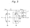
- Fig.3 shows the constitution of a transfer gate circuit according to a first embodiment of the present invention, in which portions corresponding to those in Fig. 1 are given the same reference symbols as in Fig. 1.
- Q 2 , Q 3 , 0 4 , and Qs are P-channel MOS transistors (in general, MIS transistors), which P-channel transistors are given the 0 mark in the figure.
- Q 1 , Qs , and Q 7 are N channel MOS transistors (in general, MIS transistors).
- the P-channel transistor Q 6 and N-channel transistor Q 7 comprise an inverter circuit (corresponding to the inverter circuit in Fig. 1).
- An input signal A is supplied from the output side of the inverter circuit to the N-channel transistor Q 1 comprising the transfer gate.
- the control clock signal ⁇ supplied to the gate of the transistor Qi becomes the high level, the potential of the input signal A is transferred to the output side of the transfer gate as the output potential V.
- the transfer gate is comprised by a single transistor (that is, the N-channel transistor Q 1 in the case of Fig. 3), even if a potential difference occurs based on the above wiring resistance R and the power current flowing through the above-mentioned power supply line, the chance of occurrence of the above-mentioned latch-up as in the previous cireuit comprises of the CMOS type transfer gate is completely eliminated.
- both the inverted signal A supplied to the gate of the transistor Q 2 and the inverted signal ⁇ supplied to the gate of the transistor Q 3 become low level, both the P-channel transistor Q 2 and Q 3 are turned on, and the potential of the output side of the transfer gate transistor Q 1 is made the V cc2 level, which can substantially be estimated (considered) as a high signal level.
- the signal lever it is possible to ignore the potential difference caused by the above-mentioned power supply line and the high level potential of the transfer destination is guaranteed to be made the high level potential of V cc2 which can be estimated as the high signal level.
- the inverter circuit X for supplying the above-mentioned inverted signal A to the gate of the transistor 0 2 is connected to the input side of the transistor Qt , but the inverter circuit X clearly may also be connected to the output side of the transistor Qi.
- the transistor Q 1 comprising the transfer gate was made an N-channel transistor, but the transistor Q 1 may also be made a P-channel transistor, in accordance with which the transistors Q 2 and Q 3 are made N-channel transistors and these transistors Q 2 and Q 3 are connected in series between the output side of the transistor Q 1 and the ground, whereby it is possible to supply a predetermined gate signal to these transistors Q z and Q 3 , in the similar way as above and to guarantee the low level potential of the transfer destination.
- FIG. 4 shows the constitution of a transfer gate circuit according to a second embodiment of the present invention.
- a P-channel MOS transistor Q 8 and an N-channel MOS transistor Q 9 (in general, MIS transistors) comprise another inverter circuit for supplying the inverted clock signal ⁇ of the clock signal ⁇ generated from a clock generator C to the gate of the transfer gate transistor Q 1 .
- a source side of the P-channel transistor Q 8 is connected to the power supply line at the connecting point adjacent to that of the above inverter circuit X (i.e., the connecting point having the potential level substantially equal to V CC2 ).
- the potential level of a drain region of the P-channel transistor Q 2 is equal to the value V
- an N-type well (not shown) in which the P-channel transistor Q 2 is formed is supplied with the potential V cc2 , and therefore, if the potential of the control signal ⁇ becomes higher than the predetermined level as above-mentioned, the latch-up of the transistor Q 2 may occur, as in the case of the latch-up of the above-mentioned P-channel trasistor Q 3 ' provided in the circuit shown in Fig. 1.
- the potential level of ⁇ is set to be equal to V CC2 in high level side (i.e., when the P-channel transistor Q 8 having the source connected to the power supply line at the point having the potential level substantially equal to V cc2 is turned on and the N-channel transistor Q 9 is turned off).
- the output potential V i.e., the potential level ⁇ minus the threshold voltage Vth (Qi)
- V cc2 - Vth (Qi) becomes equal to V cc2 - Vth (Qi)
- the output potential V become lower than V CC2 . Therefore, according to the circuit shown in Fig. 4, it is possible to surely prevent the occurrence of the latch-up of the P-channel transistor Q 2 provided in the output level guarantee circuit Y.
- an embodiment of the present invention it is possible to obtain a transfer gate circuit which inhibits the chance of occurrence of latch-up as in the previous CMOS type transfer gate circuit and further enables reliable transfer of the input signal supplied from the input side thereof to the output side thereof in accordance with the potential level of the control clock signal supplied to the single transfer gate transistor.
Abstract
Description
- The present invention relates to a transfer gate circuit for reliably transferring an input signal supplied from an input side thereof to an utput side thereof in accordance with a control signal.
- Generally, a transfer gate circuit of this kind comprises CMOS type transfer gate transistors including a P-channel type transistor and an N-channel type transistor connected in parallel. The gates of the P-channel type transistor and the N-channel type transistor are supplied with a control clock signal and its inverted signal, respectively. When the above pair of transistors are turned on in accordance with the potential levels of the control clock signal and its inverted signal supplied thereto, an input signal supplied to the input side of the CMOS type transfer gate transistors is transferred to the output side thereof.
- Here, the reason why the transfer gate circuit comprises the above pair of transistors constructed in the CMOS form, is that if the transfer gate were comprised only of the P-channel transistor, in the low level (zero level) state of the input signal, the potential of the output side would not fall below the threshold voltage of the P-channel transistor and if the transfer gate were comprised only of the N-channel transistor, in the high level (e.g., Vcci level) state of the input signal, the potential of the output side would not rise above the value of the high level potential of the inverted control clock signal minus the threshold voltage of the N-channel transistor. On the other hand, by constructing the transfer gate in the above CMOS form, the low level and high level of the input signal can be transferred as they are to the output side in accordance with the potential level of the control clock signal. Note that the above high level potential CCC1 of the input signal is produced through an inverter circuit, for example.
- When the above pair of CMOS transistors are formed in a P-type substrate, for example, source and drain regions of the N-channel transistor are formed in the above P-type substrate, and also, source and drain regions of the P-channel transistor are formed in an N-type well formed in the P-type substrate. The input signal having the potential Vcc, in the high level side is supplied to one of the source (drain) regions of each of the N-channel and the P-channel transistors, and the above input signal is taken out as the output signal from the other source (drain) region of each of the N-channel and the P-channel transistors. Note that the N-type well in which the P-channel transistor is formed is supplied with a predetermined potential Vcc2 (as mentioned later, which is lower than VCC1) from a power supply line which is common with the above inverter circuit.
- As mentioned above, the N-type well in which is formed the P-channel transistor comprising the CMOS type transfer gate is supplied with the predetermined potential Vcc2 from the power supply line which is common with a circuit for production of the input signal to be transferred (e.g., the inverter ciccuit), but the power supply line inevitably includes a wiring resistance. Particularly, if some circuits belonging to another system, for example, are provided between the inverter circuit and the above transfer gate transistors, the length of the power supply line between the inverter circuit and the transfer gate transistors becomes relatively long, and thus, the value of the wiring resistance due to the above length of the power supply line becomes relatively high. Further when the power current is supplied to some peripheral circuits provided on the same substrate through the power supply line, the value of the power current flowing through the power supply line also becomes high. Therefore, in such a case, a relatively large potential difference occurs between the potential Vcc9 supplied from the power supply line to the inverter circuit and the potential Vcc2 supplied from the power supply line to the N-type well. The potential Vcc2 therefore becomes lower than the potential V CC1 (that is, VCC1 > Vcc2).
- On the other hand, as a current (i.e., the input signal) flowing through a signal line is small, the high level potential of the input signal supplied to the transfer gate transistors is nearly equal to the high level potential V CC1 supplied from the inverted circuit, so in the high level state of the input signal, a PN junction turns on between the source (drain) of the P-channel transistor to which the potential VCC1 is supplied and the N-type well to which the potential VCC2 is supplied. Due to this, there is a chance of occurrence of so-called latch-up by the thyristor equivalently comprised by the PNPN layers formed in the above P-type semiconductor substrate. In such a case, subsequent to this, there is the problem that current will continue to flow in the semiconductor substrate through the PNPN layers.
- The present invention addresses this problem. An embodiment of the present invention may provide a transfer gate circuit which inhibits the chance of occurrence of latch-up as in the above conventional CMOS type transfer gate circuit and further enables reliable transfer of the input signal supplied from the input side thereof to the output side thereof in accordance with the potential level of the control clock signal supplied to a gate of a single transfer gate transistor.
- According to the present invention, there is provided a transfer gate circuit comprising a first MIS transistor operable to transmit an input signal supplied from an input side thereof to an output side thereof in accordance with a control signal supplied to a gate of the first MIS transistor; an inverter circuit connected between power supply lines and operable to invert the potential of the input signal; and an output level guarantee circuit comprising second and third MIS transistors which have a conductivity type opposite to that of the first MIS transistor and are connected in series between one of the power supply lines and the output side, wherein, in use, an output signal of the inverter circuit is supplied to a gate of the second MIS transistor, an inverted signal of the control signal supplied to the gate of the first MIS transistor being supplied to a gate of the third MIS transistor.
- According to the above-mentioned constitution, the transfer gate transistor which transmits the input signal supplied from the input side thereof to the output side thereof is not comprised in the CMOS form as in the above-mentioned conventional circuit, but is comprised by a single transistor (i.e., the first MIS transistor), so the chance of occurrence of latch-up as mentioned above is eliminated.
- Further, when the potential of the input signal supplied to the first MIS transistor comprising the transfer gate transistor is a first level (e.g., high 4evel), the second and third MIS transistors are turned on and the potential of the first level of the output side of the transfer gate transistor is guaranteed. On the other hand, when the potential of the input signal supplied to the first MIS transistor becomes a second level (e.g., low level), the second MIS transistor are turned off, and the potential of the second level of the input signal is transferred to the output side through the first MIS transistor.
- Reference is made, by way of example, to the accompanying drawings in which:
- Figure 1 is a circuit diagram showing an example of the constitution of a previous transfer gate circuit;
- Fig. 2 is a diagram showing the state of formation of the CMOS type transfer gate transistors shown in Fig. 1 in a semiconductor substrate;
- Fig. 3 is a circuit diagram showing the constitution of a transfer gate circuit according to a first embodiment of the present invention; and
- Fig. 4 is a circuit diagram showing the constitution of a transfer gate circuit according to a second embodiment of the present invention.
- In order to clarify the background of the present invention, an example of the constitution of a previously proposed transfer gate circuit is shown in Fig. 1. Namely, in Fig. 1, reference symbols Q6 and Q3' are P-channel MOS transistors (in general, MIS transistors). These P-channel transistors are given the 0 mark in the figure. Further, Q7 and Q1 are N-channel MOS transistors (in general MIS transistors). The P-channel transistor Q6 and N-channel transistor 07 comprise an inverter circuit On the other hand, the P channel transistor Q3' and N channel transistor Q1 comprise CMOS type transfer gate transistors. The potential of the input signal A supplied to the input side of the inverter circuit comprised of the transistors Q6 and Q7 is inverted by the inverter circuit. The inverted signal A is supplied to the input side of the transfer gate transistors. The gates of the transistors Q3' and Q1 are supplied with control clock signal ¢ and its inverted signal
φ . When the clock signal φ becomes the low level (therefore the inverted signal ø becomes the high level), the transistors Q3' and Q1 are turned on and the signal A having a predetermined potential supplied to the input side is transferred to the output side of the transfer gate transistors as the output potential V. Here, the reason why the transfer gate is comprised in a so-called CMOS form by the P-channel transistor Q3'. and N-channel transistor Q1 is that if the transfer gate were comprised only of the P-channel transistor Q3', in the low level (zero level) state of the input signal A , the potential of the output side would not fall below the threshold voltage Vth (Q3') of the transistor Q3' and if the transfer gate were comprised only of the N-channel transistor Qi , in the high level (level of potential VCC1 supplied from the inverter circuit) state of the input signal A , the potential of the output side would not rise above the value of the high level potential of the inverted control signal φ minus the threshold voltage Vth (Qi) of the transistor Qi. On the other hand, by constructing the transfer gate in the so called CMOS form, the low level and high level of the input signal A can be transferred as they are to the output side by the control clock signals φ and - Figure 2 shows the state of the above-mentioned transistors Q1 and Q3' formed in a semiconductor substrate. In a P-type substrate 1 are formed source (drain) regions (N-type region) 11 and 12 of the N-channel transistor Q1. In an N-
type well 2 formed in said P-type substrate 1 are formed source (drain) regions (P-type regions) 21 and 22 of the P-channel transistors Q3'. The input signal A is supplied to the N-type region 11 and the P-type region 21. By the control clock signal, these transistors Q1 and Q3' are turned on, whereby the input signal A is taken out as the output potential V from the N-type region 12 and the P-type region 22. Note that the N-tupe well 2 in which the P-channel transistor Q3' is formed is supplied with a predetermined potential V CC2 (as mentioned later, which is lower than CCC1) from a power supply line which is common with the inverter circuit. - As mentioned above, the N-
type well 2 in which is formed the P-channel transistor Q3' comprising the CMOS type transfer gate is supplied with the predetermined potential Vcc2 from the power supply line which is common with a circuit for production of the input signal A to be transferred (in the above-mentioned Fig. 1, the inverter circuit), but the power supply line inevitably includes a wiring resistance R. Particularly, if some circuits belonging to another system, for example, are provided between the inverter circuit and the transfer gate transistors, the length of the power supply line becomes relatively long, and accordingly, the value of the wiring resistance R becomes relatively high. Further, when the power current is supplied to some peripheral circuits (not shown) provided on the same substrate through the power supply line, the value of the power current flowing through the power supply line also becomes high. Therefore, in such a case, relatively large potential difference occurs between the potential VCC1 supplied from the power supply line to the inverter circuit and the potential Vcc2 supplied from the power supply line to the N-type well. The potential VCC2 therefore becomes lower than the potential V CC1 (that is, VCC1 > Vcc2). - On the other hand, as the current flowing through the signal line is small the high level potential of the input signal A supplied to the transfer gate transistors is nearly equal to the high level potential VCC1 supplied from the inverter circuit, so in the high level state of the input signal A , a PN junction turns on between the source (or drain) of the P-channel transistor Q3' to which the potential VCC1 is supplied and the N-
type well 2 to which the potential VCC2 is supplied. Due to this, there is a chance of occurrence of so-called latch-up by the thyristor equivalently comprised by the PNPN layers formed in the semiconductor substrate. In such a case, subsequent to this, there is the problem that current will continue to flow in the semiconductor substrate through the PNPN layers. - The present invention addresses this problem, and Fig.3 shows the constitution of a transfer gate circuit according to a first embodiment of the present invention, in which portions corresponding to those in Fig. 1 are given the same reference symbols as in Fig. 1. In Figs. 3, Q2, Q3, 04 , and Qs are P-channel MOS transistors (in general, MIS transistors), which P-channel transistors are given the 0 mark in the figure. Further, Q1, Qs , and Q7 are N channel MOS transistors (in general, MIS transistors).
- The P-channel transistor Q6 and N-channel transistor Q7 comprise an inverter circuit (corresponding to the inverter circuit in Fig. 1). An input signal A is supplied from the output side of the inverter circuit to the N-channel transistor Q1 comprising the transfer gate. When the control clock signal
φ supplied to the gate of the transistor Qi becomes the high level, the potential of the input signal A is transferred to the output side of the transfer gate as the output potential V. - Between the power source line which is common with the inverter circuit and the output side of the transfer gate transistor Q1 are connected in series two P-channel (that is, conductivities opposite to the above-mentioned N-channel transistor Qi) transistors Q2 and Q3. To the gate of the transistor Q2 is supplied a signal A inverted by an inverter circuit X comprised of the transistors Q4 and Q5 from an input signal A supplied to the N-channal transistor Qi. On the other hand, a clock signal φ inverted from a control clock signal
φ supplied to the gate of the N-channel transistor Qi is supplied to the gate of the transistor Q3. Here, these two transistors Q2 and Q3 comprise an output level guarantee circuit Y, so the high level potential transferred to the output side of the transfer gate (N-channel transistor Qi) is guaranteed by the output level guarantee circuit Y. - In such a transfer gate circuit of the present invention described above, since the transfer gate is comprised by a single transistor (that is, the N-channel transistor Q1 in the case of Fig. 3), even if a potential difference occurs based on the above wiring resistance R and the power current flowing through the above-mentioned power supply line, the chance of occurrence of the above-mentioned latch-up as in the previous cireuit comprises of the CMOS type transfer gate is completely eliminated.
- Further, at the high level state of the input signal
A (that is, the VCC1 level), when the control clock signalφ becomes the high level, it is not possible to transfer the predetermined high level potential as mentioned above by just the above-mentioned N-channel transistor Qi, but in the present invention, both the inverted signal A supplied to the gate of the transistor Q2 and the inverted signal φ supplied to the gate of the transistor Q3 become low level, both the P-channel transistor Q2 and Q3 are turned on, and the potential of the output side of the transfer gate transistor Q1 is made the Vcc2 level, which can substantially be estimated (considered) as a high signal level. Namely, when considering the signal lever, it is possible to ignore the potential difference caused by the above-mentioned power supply line and the high level potential of the transfer destination is guaranteed to be made the high level potential of Vcc2 which can be estimated as the high signal level. - On the other hand, in the low level state of the input signal A (that is, the zero level), when the control clock signal
φ becomes the high level and the transistor Q1 is turned on, the transistor Q2 is turned off and the low level potential of the transfer destination is made equal to the ground potential through the transistor Q1 and the transistor Q7. - Note that in the illustrated embodiment, the inverter circuit X for supplying the above-mentioned inverted signal A to the gate of the transistor 02 is connected to the input side of the transistor Qt , but the inverter circuit X clearly may also be connected to the output side of the transistor Qi.
- Further, in the illustrated embodiment, the transistor Q1 comprising the transfer gate was made an N-channel transistor, but the transistor Q1 may also be made a P-channel transistor, in accordance with which the transistors Q2 and Q3 are made N-channel transistors and these transistors Q2 and Q3 are connected in series between the output side of the transistor Q1 and the ground, whereby it is possible to supply a predetermined gate signal to these transistors Qz and Q3 , in the similar way as above and to guarantee the low level potential of the transfer destination.
- Figure 4 shows the constitution of a transfer gate circuit according to a second embodiment of the present invention. In this embodiment, a P-channel MOS transistor Q8 and an N-channel MOS transistor Q9 (in general, MIS transistors) comprise another inverter circuit for supplying the inverted clock signal
φ of the clock signal φ generated from a clock generator C to the gate of the transfer gate transistor Q1. Note that in the transfer gate circuit shown in Fig. 4, portions corresponding to those in Fig. 3 are given the same reference symbols as in Fig. 3. In this connection, a source side of the P-channel transistor Q8 is connected to the power supply line at the connecting point adjacent to that of the above inverter circuit X (i.e., the connecting point having the potential level substantially equal to VCC2 ). In this connection, if the potential of the control clock signalφ becomes high level, which is higher than a predetermined level from one cause or another (e.g., if the potential level of the clock signalφ becomes the above VCC1 plus the above threshold voltage Vth (Qi), and the output potential V becomes equal to VCC1 which is higher than Vcc2), there is a chance of occurrence of the latch-up of the P-channel transistor Q2 provided in the output level guarantee circuit Y. - In more detail, the potential level of a drain region of the P-channel transistor Q2 is equal to the value V, an N-type well (not shown) in which the P-channel transistor Q2 is formed is supplied with the potential Vcc2 , and therefore, if the potential of the control signal
φ becomes higher than the predetermined level as above-mentioned, the latch-up of the transistor Q2 may occur, as in the case of the latch-up of the above-mentioned P-channel trasistor Q3' provided in the circuit shown in Fig. 1. - However, in the above circuit shown in Fig. 4, the potential level of
φ is set to be equal to VCC2 in high level side (i.e., when the P-channel transistor Q8 having the source connected to the power supply line at the point having the potential level substantially equal to Vcc2 is turned on and the N-channel transistor Q9 is turned off). Thus, the output potential V (i.e., the potential levelφ minus the threshold voltage Vth (Qi)) becomes equal to Vcc2 - Vth (Qi)), and as a result, the output potential V become lower than VCC2. Therefore, according to the circuit shown in Fig. 4, it is possible to surely prevent the occurrence of the latch-up of the P-channel transistor Q2 provided in the output level guarantee circuit Y. - As above-mentioned, by an embodiment of the present invention, it is possible to obtain a transfer gate circuit which inhibits the chance of occurrence of latch-up as in the previous CMOS type transfer gate circuit and further enables reliable transfer of the input signal supplied from the input side thereof to the output side thereof in accordance with the potential level of the control clock signal supplied to the single transfer gate transistor.
Claims (7)
Applications Claiming Priority (2)
| Application Number | Priority Date | Filing Date | Title |
|---|---|---|---|
| JP219837/86 | 1986-09-19 | ||
| JP61219837A JPS6376472A (en) | 1986-09-19 | 1986-09-19 | Transfer gate circuit |
Publications (3)
| Publication Number | Publication Date |
|---|---|
| EP0261879A2 true EP0261879A2 (en) | 1988-03-30 |
| EP0261879A3 EP0261879A3 (en) | 1989-05-24 |
| EP0261879B1 EP0261879B1 (en) | 1991-11-27 |
Family
ID=16741826
Family Applications (1)
| Application Number | Title | Priority Date | Filing Date |
|---|---|---|---|
| EP87308246A Expired - Lifetime EP0261879B1 (en) | 1986-09-19 | 1987-09-17 | Transfer gate circuit |
Country Status (5)
| Country | Link |
|---|---|
| US (1) | US4806795A (en) |
| EP (1) | EP0261879B1 (en) |
| JP (1) | JPS6376472A (en) |
| KR (1) | KR910002503B1 (en) |
| DE (1) | DE3774816D1 (en) |
Families Citing this family (4)
| Publication number | Priority date | Publication date | Assignee | Title |
|---|---|---|---|---|
| US5705940A (en) * | 1990-07-16 | 1998-01-06 | Raytheon Company | Logic family for digitally controlled analog monolithic microwave integrated circuits |
| JP3151329B2 (en) * | 1993-04-07 | 2001-04-03 | 株式会社東芝 | Data output circuit |
| JPH0865135A (en) * | 1994-08-17 | 1996-03-08 | Fujitsu Ltd | Output buffer circuit |
| US5736887A (en) * | 1996-01-25 | 1998-04-07 | Rockwell International Corporation | Five volt tolerant protection circuit |
Citations (3)
| Publication number | Priority date | Publication date | Assignee | Title |
|---|---|---|---|---|
| US3675144A (en) * | 1969-09-04 | 1972-07-04 | Rca Corp | Transmission gate and biasing circuits |
| JPS54128262A (en) * | 1978-03-29 | 1979-10-04 | Hitachi Ltd | Complementary mis inverter circuit |
| EP0115834A2 (en) * | 1983-01-29 | 1984-08-15 | Kabushiki Kaisha Toshiba | Racefree CMOS clocked logic circuit |
Family Cites Families (1)
| Publication number | Priority date | Publication date | Assignee | Title |
|---|---|---|---|---|
| US4563599A (en) * | 1983-03-28 | 1986-01-07 | Motorola, Inc. | Circuit for address transition detection |
-
1986
- 1986-09-19 JP JP61219837A patent/JPS6376472A/en active Granted
-
1987
- 1987-09-16 US US07/097,557 patent/US4806795A/en not_active Expired - Fee Related
- 1987-09-17 DE DE8787308246T patent/DE3774816D1/en not_active Expired - Fee Related
- 1987-09-17 EP EP87308246A patent/EP0261879B1/en not_active Expired - Lifetime
- 1987-09-18 KR KR1019870010347A patent/KR910002503B1/en not_active IP Right Cessation
Patent Citations (3)
| Publication number | Priority date | Publication date | Assignee | Title |
|---|---|---|---|---|
| US3675144A (en) * | 1969-09-04 | 1972-07-04 | Rca Corp | Transmission gate and biasing circuits |
| JPS54128262A (en) * | 1978-03-29 | 1979-10-04 | Hitachi Ltd | Complementary mis inverter circuit |
| EP0115834A2 (en) * | 1983-01-29 | 1984-08-15 | Kabushiki Kaisha Toshiba | Racefree CMOS clocked logic circuit |
Non-Patent Citations (3)
| Title |
|---|
| IT/INFORMATIONSTECHNIK, vol. 28, no. 3, 1986, pages 142-129, Munich, DE; N. WEHN et al.: "Statische und dynamische CMOS-schaltungstechniken im Vergleich" * |
| JOURNAL OF SOLID-STATE CIRCUITS, vol. SC-8, no. 6, december 1973, pages 462-468; Y. SUZUKI et al.: "Clocked CMOS calculator circuitry" * |
| PATENT ABSTRACTS OF JAPAN, vol. 3, no. 149 (E-157), 8th December 1979, page 67 E 157; & JP-A-54 128 262 (HITACHI SEISAKUSHO K.K.) 19-04-1979 * |
Also Published As
| Publication number | Publication date |
|---|---|
| KR880004655A (en) | 1988-06-07 |
| DE3774816D1 (en) | 1992-01-09 |
| EP0261879B1 (en) | 1991-11-27 |
| JPH0257345B2 (en) | 1990-12-04 |
| JPS6376472A (en) | 1988-04-06 |
| US4806795A (en) | 1989-02-21 |
| KR910002503B1 (en) | 1991-04-23 |
| EP0261879A3 (en) | 1989-05-24 |
Similar Documents
| Publication | Publication Date | Title |
|---|---|---|
| US4039869A (en) | Protection circuit | |
| US5341034A (en) | Backup battery power controller having channel regions of transistors being biased by power supply or battery | |
| KR100302535B1 (en) | SOI type semiconductor device and bias voltage generator with variable threshold voltage | |
| US6437627B1 (en) | High voltage level shifter for switching high voltage in non-volatile memory intergrated circuits | |
| KR960003226B1 (en) | Input/output buffer circuit | |
| KR0136233B1 (en) | Interface circuit | |
| JPH03235517A (en) | Switching circuit | |
| US6184716B1 (en) | High voltage output stage for driving an electric load | |
| US5239211A (en) | Output buffer circuit | |
| US6188243B1 (en) | Input/output circuit with high input/output voltage tolerance | |
| US4833347A (en) | Charge disturbance resistant logic circuits utilizing true and complement input control circuits | |
| US4591742A (en) | Output circuit capable of being connected to another circuit having transistors of any conduction type | |
| EP0261879A2 (en) | Transfer gate circuit | |
| US4081699A (en) | Depletion mode coupling device for a memory line driving circuit | |
| JPH11355117A (en) | Integrated circuit containing cmos input buffer protection circuit | |
| KR940004455B1 (en) | Cmos semiconductor intrgrated circuit device | |
| US6288586B1 (en) | Circuit for standby current reduction | |
| KR0142001B1 (en) | Mosfet interface circuit having an increased or a reduced mutual conductance | |
| US5969563A (en) | Input and output circuit with wide voltage tolerance | |
| US6269042B1 (en) | I/O circuit of semiconductor integrated device | |
| JP2978346B2 (en) | Input circuit of semiconductor integrated circuit device | |
| US6545506B1 (en) | CMOS output driver that can tolerant a high input voltage | |
| US3965367A (en) | Multiple output logic circuits | |
| US6218867B1 (en) | Pass transistor circuit | |
| US6404016B1 (en) | Semiconductor device |
Legal Events
| Date | Code | Title | Description |
|---|---|---|---|
| PUAI | Public reference made under article 153(3) epc to a published international application that has entered the european phase |
Free format text: ORIGINAL CODE: 0009012 |
|
| AK | Designated contracting states |
Kind code of ref document: A2 Designated state(s): DE FR GB |
|
| PUAL | Search report despatched |
Free format text: ORIGINAL CODE: 0009013 |
|
| AK | Designated contracting states |
Kind code of ref document: A3 Designated state(s): DE FR GB |
|
| 17P | Request for examination filed |
Effective date: 19890712 |
|
| 17Q | First examination report despatched |
Effective date: 19900329 |
|
| GRAA | (expected) grant |
Free format text: ORIGINAL CODE: 0009210 |
|
| AK | Designated contracting states |
Kind code of ref document: B1 Designated state(s): DE FR GB |
|
| REF | Corresponds to: |
Ref document number: 3774816 Country of ref document: DE Date of ref document: 19920109 |
|
| ET | Fr: translation filed | ||
| PLBE | No opposition filed within time limit |
Free format text: ORIGINAL CODE: 0009261 |
|
| STAA | Information on the status of an ep patent application or granted ep patent |
Free format text: STATUS: NO OPPOSITION FILED WITHIN TIME LIMIT |
|
| 26N | No opposition filed | ||
| PGFP | Annual fee paid to national office [announced via postgrant information from national office to epo] |
Ref country code: GB Payment date: 19930713 Year of fee payment: 7 |
|
| PGFP | Annual fee paid to national office [announced via postgrant information from national office to epo] |
Ref country code: FR Payment date: 19930929 Year of fee payment: 7 |
|
| PGFP | Annual fee paid to national office [announced via postgrant information from national office to epo] |
Ref country code: DE Payment date: 19931121 Year of fee payment: 7 |
|
| PG25 | Lapsed in a contracting state [announced via postgrant information from national office to epo] |
Ref country code: GB Effective date: 19940917 |
|
| GBPC | Gb: european patent ceased through non-payment of renewal fee |
Effective date: 19940917 |
|
| PG25 | Lapsed in a contracting state [announced via postgrant information from national office to epo] |
Ref country code: FR Effective date: 19950531 |
|
| PG25 | Lapsed in a contracting state [announced via postgrant information from national office to epo] |
Ref country code: DE Effective date: 19950601 |
|
| REG | Reference to a national code |
Ref country code: FR Ref legal event code: ST |