EP0260956A2 - Photoelectric converting apparatus - Google Patents
Photoelectric converting apparatus Download PDFInfo
- Publication number
- EP0260956A2 EP0260956A2 EP87308201A EP87308201A EP0260956A2 EP 0260956 A2 EP0260956 A2 EP 0260956A2 EP 87308201 A EP87308201 A EP 87308201A EP 87308201 A EP87308201 A EP 87308201A EP 0260956 A2 EP0260956 A2 EP 0260956A2
- Authority
- EP
- European Patent Office
- Prior art keywords
- line
- signal
- photoelectric converting
- converting apparatus
- scanning
- Prior art date
- Legal status (The legal status is an assumption and is not a legal conclusion. Google has not performed a legal analysis and makes no representation as to the accuracy of the status listed.)
- Granted
Links
- 239000003990 capacitor Substances 0.000 claims description 22
- 238000006243 chemical reaction Methods 0.000 claims description 16
- 230000003321 amplification Effects 0.000 claims description 4
- 238000003199 nucleic acid amplification method Methods 0.000 claims description 4
- 230000008878 coupling Effects 0.000 claims 3
- 238000010168 coupling process Methods 0.000 claims 3
- 238000005859 coupling reaction Methods 0.000 claims 3
- 238000010586 diagram Methods 0.000 description 10
- 230000035508 accumulation Effects 0.000 description 6
- 238000009825 accumulation Methods 0.000 description 6
- 238000000034 method Methods 0.000 description 5
- 239000000969 carrier Substances 0.000 description 4
- 239000012535 impurity Substances 0.000 description 4
- 230000000875 corresponding effect Effects 0.000 description 3
- VYPSYNLAJGMNEJ-UHFFFAOYSA-N Silicium dioxide Chemical compound O=[Si]=O VYPSYNLAJGMNEJ-UHFFFAOYSA-N 0.000 description 2
- 230000009467 reduction Effects 0.000 description 2
- 239000004065 semiconductor Substances 0.000 description 2
- 239000000758 substrate Substances 0.000 description 2
- 229910052581 Si3N4 Inorganic materials 0.000 description 1
- XUIMIQQOPSSXEZ-UHFFFAOYSA-N Silicon Chemical compound [Si] XUIMIQQOPSSXEZ-UHFFFAOYSA-N 0.000 description 1
- 230000008859 change Effects 0.000 description 1
- 229910052681 coesite Inorganic materials 0.000 description 1
- 239000000470 constituent Substances 0.000 description 1
- 238000010276 construction Methods 0.000 description 1
- 230000001276 controlling effect Effects 0.000 description 1
- 229910052906 cristobalite Inorganic materials 0.000 description 1
- 238000009792 diffusion process Methods 0.000 description 1
- 230000000694 effects Effects 0.000 description 1
- 238000000407 epitaxy Methods 0.000 description 1
- 230000006698 induction Effects 0.000 description 1
- 230000010354 integration Effects 0.000 description 1
- 238000005468 ion implantation Methods 0.000 description 1
- 238000002955 isolation Methods 0.000 description 1
- 229910021420 polycrystalline silicon Inorganic materials 0.000 description 1
- 229920005591 polysilicon Polymers 0.000 description 1
- 230000003252 repetitive effect Effects 0.000 description 1
- 230000004044 response Effects 0.000 description 1
- 230000035945 sensitivity Effects 0.000 description 1
- 229910052710 silicon Inorganic materials 0.000 description 1
- 239000010703 silicon Substances 0.000 description 1
- 239000000377 silicon dioxide Substances 0.000 description 1
- 235000012239 silicon dioxide Nutrition 0.000 description 1
- 230000003068 static effect Effects 0.000 description 1
- 229910052682 stishovite Inorganic materials 0.000 description 1
- 229910052905 tridymite Inorganic materials 0.000 description 1
Images


Classifications
-
- H—ELECTRICITY
- H04—ELECTRIC COMMUNICATION TECHNIQUE
- H04N—PICTORIAL COMMUNICATION, e.g. TELEVISION
- H04N25/00—Circuitry of solid-state image sensors [SSIS]; Control thereof
- H04N25/40—Extracting pixel data from image sensors by controlling scanning circuits, e.g. by modifying the number of pixels sampled or to be sampled
- H04N25/41—Extracting pixel data from a plurality of image sensors simultaneously picking up an image, e.g. for increasing the field of view by combining the outputs of a plurality of sensors
-
- H—ELECTRICITY
- H01—ELECTRIC ELEMENTS
- H01L—SEMICONDUCTOR DEVICES NOT COVERED BY CLASS H10
- H01L27/00—Devices consisting of a plurality of semiconductor or other solid-state components formed in or on a common substrate
- H01L27/14—Devices consisting of a plurality of semiconductor or other solid-state components formed in or on a common substrate including semiconductor components sensitive to infrared radiation, light, electromagnetic radiation of shorter wavelength or corpuscular radiation and specially adapted either for the conversion of the energy of such radiation into electrical energy or for the control of electrical energy by such radiation
- H01L27/144—Devices controlled by radiation
- H01L27/146—Imager structures
- H01L27/14681—Bipolar transistor imagers
-
- H—ELECTRICITY
- H04—ELECTRIC COMMUNICATION TECHNIQUE
- H04N—PICTORIAL COMMUNICATION, e.g. TELEVISION
- H04N25/00—Circuitry of solid-state image sensors [SSIS]; Control thereof
- H04N25/70—SSIS architectures; Circuits associated therewith
- H04N25/701—Line sensors
-
- H—ELECTRICITY
- H04—ELECTRIC COMMUNICATION TECHNIQUE
- H04N—PICTORIAL COMMUNICATION, e.g. TELEVISION
- H04N3/00—Scanning details of television systems; Combination thereof with generation of supply voltages
- H04N3/10—Scanning details of television systems; Combination thereof with generation of supply voltages by means not exclusively optical-mechanical
- H04N3/14—Scanning details of television systems; Combination thereof with generation of supply voltages by means not exclusively optical-mechanical by means of electrically scanned solid-state devices
- H04N3/15—Scanning details of television systems; Combination thereof with generation of supply voltages by means not exclusively optical-mechanical by means of electrically scanned solid-state devices for picture signal generation
- H04N3/1581—Scanning details of television systems; Combination thereof with generation of supply voltages by means not exclusively optical-mechanical by means of electrically scanned solid-state devices for picture signal generation using linear image-sensor
Definitions
- the present invention relates to a photoelectric converting apparatus of the type having a plurality of photosensors and a plurality of signal output lines for picking up signals from the photosensors, wherein the signals are picked up through signal output terminals smaller in number than that of the signal output lines.
- Fig. l is a circuit diagram showing one example of a conventional photoelectric converting apparatus.
- sensor line blocks l0l and l02 each constructed of one-dimensionally disposed photosensors. Signals from each sensor line block is sequentially read via signal output lines l03 and l04 which are commonly connected to an amplifier l05 having a signal output terminal l06. During reading signals from one sensor line blocks, reading signals from the other line sensor block is inhibited. Thus, signals from the two signal output lines can be read via the single output terminal, resulting in less number of wirings to external circuitry.
- signal from the sensor line blocks l0l and l02 are temporarily stored in charge storage capacitors or wiring capacitance Cl to Cn.
- Signals from the sensor line blocks l0l and l02 are sequentially picked up to the signal output lines l03 and l04, respectively under control of shift registers.
- the signals are then outputted via the amplifier l05 at its signal output terminal l06.
- each wiring capacitance Cwl and Cw2 of the signal output line are added together, resulting in a large capacitance of each signal output line.
- the output of a signal stored, for example, in the charge storage capacitor Cl is reduced at the signal output line l03 by the large capacitance.
- a photoelectric converting apparatus of the type having a plurality of photosensors and a plurality of signal output lines for picking up signals from the photosensors, wherein the signals are picked up through signal output terminals smaller in number than that of the signal output lines
- the photoelectric converter is characterized by that the signal output lines each have switch means for switching the signal output line and connecting a desired output line to a signal output terminal.
- the drive frequency of selection means may use a lower frequency in case where a high frequency operation becomes necessary for a great number of photosensors, thus enabling a high degree of freedom in circuit design, pattern design for semiconductor devices and the like.
- each signal output line is connected to the signal output terminal via switch means, the wiring capacity of the signal output line from which a signal is picked up via the closed switch means can be greatly reduced by opening the other switch means. Therefore, reduction in signal level at the signal output line can be avoided, and an image pickup apparatus with a high resolution and high output can be easily realized.
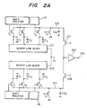
- Fig. 2A is a schematic circuit diagram showing an embodiment of the photoelectric converting apparatus according to the present invention.
- a signal output line l03 from which signals from a sensor line block l0l are sequentially outputted is connected to the input terminal of an amplifier l05 via switch means l07.
- a signal output line l04 from which signals from a sensor line block l02 are sequentially outputted is connected to the input terminal of the amplifier l05 via switch means l08.
- MOS transistors are used as switch means in this embodiment. However, other devices having a low conductive resistance such as analog switches may obviously be used.
- a larger number of signal output lines may be commonly connected to the input terminal of the amplifier l05 via switch means.
- Fig. 2B is a schematic cross section of a photoelectric conversion cell disclosed in Japanese Patent Laid-open Gazettes Nos. l2759/l985 and l2765/l985, and Fig. 2C is an equivalent circuit of the photoelectric conversion cell.
- each photosensor cell is formed on an n+ silicon substrate l and electrically isolated from adjacent photosensor cells by an element isolation region 2 made of, for example, SiO2, Si3N4, polysilicon or the like.
- Each photosensor cell has the following constituent elements: A p-region 4 is formed by doping p-type impurity on an n ⁇ -region 3 of low impurity concentration formed by the epitaxy method or the like. An n+-region 5 is formed in the p-region l04 by the impurity diffusion method, the ion implantation method or the like. The p-region 4 and n+-region 5 serve as the base and emitter of a bipolar transistor, respectively.
- a capacitor electrode 7 Formed on an oxide film 6 deposited on the n ⁇ -region 3 with the above regions is a capacitor electrode 7 of predetermined area which faces the p-region 4 with the oxide film 6 interposed therebetween.
- the potential of the p-region l04 in a floating state is controlled by a pulse voltage applied to the capacitor electrode 7.
- the photosensor cell is constructed further of an emitter electrode 8 connected to the n+-region 5, an n+-region ll of high impurity concentration formed on the substrate l, and an electrode l2 supplying a potential to the collector of the bipolar transistor.
- a readout positive pulse is applied to the capacitor electrode 7 so that a readout signal corresponding to a change in base potential during the accumulation operation is outputted from the emitter electrode (readout operation). Repetitive readout operations are possible because the accumulated charge amount in the base p-region 4 does not decrease to large extent.
- the emitter electrode 8 is grounded and the capacitor electrode 8 is applied with a positive refresh pulse. With this pulse applied, the p-region 4 is forward biased relative to the n+ region 5 so that accumulated holes are removed. At the trailing edge of the refresh pulse, the p-region 4 takes again its initial negative potential (refresh operation). Thereafter, similar accumulation, readout and refresh operations are repeated.
- light-induced carriers are accumulated in the base p-region 4 to control a current passing through the emitter and collector electrodes 8 and l2 in accordance with the accumulated charge quantity.
- the accumulated carriers are read after amplifying them by the amplification function of each cell, thereby achieving a high output and sensitivity, and less noises.
- the potential V p of the base with light-induced carriers (holes in this case) accumulated therein is given by Q/C, wherein Q represents the charge of carriers accumulated in the base region, and C represents a capacitor coupled to the base region.
- Q represents the charge of carriers accumulated in the base region
- C represents a capacitor coupled to the base region.
- Fig. 3A is a circuit diagram showing an example of a driver for the sensor line block using the above photoelectric conversion cells
- Fig. 3B is a timing chart for explaining the operation of the driver circuit.
- each collector electrode l2 of the photoelectric conversion cells Sl to Sn is applied with a predetermined voltage.
- Capacitor electrodes 7 are connected in common to a terminal ll0 to which a signal ⁇ 1 for the readout and refresh operations is applied.
- Each emitter electrode 8 is connected to respective vertical lines Ll to Ln which are connected to one main electrodes of respective buffer transistors Tal to Tan.
- the gate electrodes of the buffer transistors Tal to Tan are connected in common to a terminal lll to which a signal ⁇ 2 is applied.
- the other main electrodes of the buffer transistors Tal to Tan are grounded via charge storage capacitors Cl to Cn serving as accumulation means, and also connected to the signal line l03 via transistors Tl to Tn.
- the gate electrodes of the transistors Tl to Tn are respectively connected to the parallel output terminals of the shift register from which signals ⁇ hl to ⁇ hn are sequentially outputted.
- the signal output line l03 is grounded via transistor Tr for refreshing the signal output line l03.
- the gate electrode of the transistor Tr is applied with a signal ⁇ r2 .
- the vertical lines Ll to Ln are grounded via respective buffer transistors Tbl to Tbn.
- the gate electrodes of the buffer transistors Tbl to Tbn are connected in common to a terminal ll2 to which a signal ⁇ 3 is applied.
- signals ⁇ 2 and ⁇ 3 are made high level to cause the buffer transistors Tal to Tan to turn on. Therefore, the emitter electrodes 8 of the photoelectric conversion cells Sl to Sn are grounded and residual charges in the cahrge storage capacitors Cl to Cn are removed therefrom.
- signal ⁇ 1 becomes high level to apply a positive refresh voltage to the capacitor electrode 7 of each photoelectric conversion cell, a refresh operation is performed as described before.
- signal ⁇ 1 becomes low level, the base region 4 of each cell returns to its intial negative potential.
- Signals ⁇ 2 and ⁇ 3 are made low level to cause the buffer transistors Tal to Tan and Tbl to Tbn to turn off. In this condition, holes of light-induced electron/hole pairs are accumulated in the base region 4 of each photoelectric conversion cell Sl to Sn so that the base potential of each cell rises to a higher value from the initial negative potential by the accumulated potential corresponding to the incident light amount.
- signals ⁇ 1 and ⁇ 2 are made high level, signals read from the emitter electrodes 8 of the photoelectric conversion cells Sl to Sn are accumulated at the same time in the charge storage capacitors Cl to Cn via the buffer transistors Tal to Tan.
- signal ⁇ r2 is made high level to cause the transistor Tr to turn on.
- residual charge on the signal output line l03 is removed via the transistor Tr to effect a refresh operation.
- switch means l07 While the sensor line block l0l is read, switch means l07 is turned on and switch means l08 is turned off. Conversely, while the sensor line block l02 is read, switch means l07 is turned off and switch means l08 is turned on.
- photosensors are not limited to the above embodiment but the photosensors such as photoconductive type sensors, photodiodes, static induction transistors may be used.
- Fig. 4 is a block diagram showing an example of an image pickup apparatus using the above embodiment. In this case, it is needless to say that a number of sensor line blocks are provided and switch means is provided for each sensor line block.
- an image pickup device 30l has a similar construction as of the above embodiment.
- the output signal Vo therefrom is processed including a gain adjustment by a signal processing circuit 302 to output it as a standard television signal in the form of NTSC signal or the like.
- Various types of pulses for driving the image pickup device 30l are supplied from a driver 303 which is controlled by a control unit 304.
- the control unit 304 adjusts a gain and the like of the signal processing circuit 302 in accordance with an output from the image pickup device, and adjusts the incident light amount to the image pickup device 30l by controlling an exposure control unit 305.
- each signal output line of the photoelectric converter of the above embodiment according to the present invention is coupled to the output terminal via switch means. Therefore, a wiring capacitance on a signal output line from which a signal is outputted via closed switch means is greatly reduced as compared with a conventional one, by opening switch means on the other signal output lines. Hence, it is possible to prevent lowering the level of a signal outputted from the signal output line.
- Fig. 5 is a schematic circuit diagram showing an embodiment of the photoelectric converter according to the present invention.
- sensor line blocks l0l and l02 each having a plurality of n photosensors.
- Each sensor line block is intended herein to include such concept as it represents odd/even lines of a sensor group such as an area sensor, it represents odd/even photosensors on an arbitrary line, and the like.
- two sensor blocks are shown.
- n output terminals of the sensor line block l0l are connected to capacitors Cll to Cln and connected in common to a signal output line l03 via transistors Tll to Tln.
- Each gate electrode of transistor Tll to Tln is inputted with pulses ⁇ 11 to ⁇ ln from a scanning circuit ll5.
- Pulses ⁇ 31 and ⁇ 32 are inputted to input terminal a and b of the scanning circuit ll5.
- the signal line l03 is grounded via transistor Trl and connected to the input terminal of an amplifier l05 via a transistor l07 serving as switch means.
- a pulse ⁇ cl is inputted to the gate electrode of the transistor Trl, and a pulse ⁇ srl is input to the gate electrode of the transistor l07.
- the sensor line block l02 is constructed in a similar manner. N output terminals of the sensor line block l02 are connected to capacitors C2l to C2n and connected in common to a signal output line l04 via transistors T2l to Tln. Each gate electrode of transistor T2l to T2n is inputted with pulse ⁇ 21 to ⁇ 2n from a scanning circuit ll6. Pulses ⁇ 32 and ⁇ 31 are inputted to inputted to input terminal a and b of the scanning circuit ll6, as opposed to the case of the scanning circuit ll5.
- the signal line l04 is grounded via transistor Tr2 and connected to the input terminal of the amplifier l05 via a transistor l08 serving as switch means.
- a pulse ⁇ c2 is inputted to the gate electrode of the transistor Tr2, and a pulse ⁇ sr2 is inputted to the gate electrode of the transistor l08.
- Fig. 6 is a timing chart illustrating the operation of the scanning circuit.
- the scanning circuits ll5 and ll6 are two-phase driven by pulses ⁇ 31 and ⁇ 32. With the interconnection shown in Fig. 5, pulses ⁇ 11 to ⁇ ln are outputted from the scanning circuit ll5 in synchro with the pulse ⁇ 31, whereas pulses ⁇ 21 to ⁇ 2n are outputted from the scanning circuit ll6 in synchro with the pulse ⁇ 32, respectively as shown in the timing chart. Therefore, based on the timings of pulses ⁇ 31 and ⁇ 32, the scanning circuits ll5 and ll6 can independently or alternately be operated at desired timings.
- the above-described various pulses are supplied from a driver ll7 which outputs a pulse at the timing in synchro with a clock signal from an oscillator ll8.
- Transistors l07 and l08 are used as switch means in this embodiment. However, obviously other devices having a low conductive resistance such as analog switches may be used similar to the embodiment shown in> Fig. 2.
- the invention includes the arrangement wherein three or more sensor line blocks are provided and the signal output lines are connected in common to the input terminal of the amplifier l09 via respective switch means.
- Fig. 7 shows a timing chart illustrating a first example of timings of pulses outputted from the driver ll7.
- pulse ⁇ srl is made high level and pulse ⁇ sr2 is made low level to turn on the transistor l07 and turn off the transistor l08.
- pulse ⁇ 11 is outputted from the scanning circuit ll5 to turn on the transistor Tll.
- a signal at the first cell of the sensor line block l0l is picked up from the capacitor Cll onto the signal output line l03, and hence to the external circuit via the transistor l07, the amplifier l05 and the output terminal l06.
- pulse ⁇ c2 is made high level to turn on the transistor Tr2 so that residual charge on the signal output line l04 is removed.
- pulses ⁇ srl and ⁇ sr2 are inverted respectively to low level and high level to turn off the transistor l07 and turn on the transistor l08.
- pulse ⁇ 21 is outputted from the scanning circuit ll6 to turn on the transistor T2l. Then a signal at the first cell of the sensor line block l02 is picked up from the capacitor C2l onto the signal output line l04, and hence to the external circuit via the transistor l08 and the amplifier l05.
- pulse ⁇ cl is made high level to turn on the transistor Trl and remove residual charge present at the preceding signal on the signal output line l03.
- signals from the sensors in the sensor line blocks l0l and l02 are alternately and sequentially outputted to the external circuit in response to pulses ⁇ 12 to ⁇ ln from the scanning circuit ll5 and pulses ⁇ 22 to ⁇ 2n from the scanning circuit ll6.
- the wiring capacitance on a signal output line from which a signal is read is substantially the wiring capacitance Cw of the line itself because one of the transistors l07 and l08 from which a signal is not read is made turned off.
- each sensor line block l0l and l02 is provided with respective scanning circuit ll5 and ll6, the scanning circuit can be driven at a lower operating frequency corresponding to n photosensors although 2n photosensors are used, thus leading to a high degree of freedom in design.
- Fig. 8 is a timing chart showing a second example of timings of pulses outputted from the driver ll7.
- photosensors in the sensor line blocks l0l and l02 are sequentially read one block at a time.
- the transistor l07 is turned on and the transistor l08 is turned off by applying pulses ⁇ srl and ⁇ sr2 .
- pulses ⁇ 11 to ⁇ ln are sequentially outputted from the scanning circuit ll5 to read all the signals from the cells in the sensor line block l0l.
- the transistor l07 is turned off and the transistor l08 is turned on to read all the signals from the sensor line block l02.
- Figs. 9 and l0 are timing charts showing the third and fourth examples of timings of pulses outputted from the driver ll7.
- signals can be read from only one of the sensor line blocks by maintaining the other scanning circuit turned off.
- selection means for selecting photosensors in sensor line blocks are provided. Therefore, even if a high frequency operation is required for a large number of photosensors, selection means can be operated at a lower frequency, resulting in a high degree of freedom in circuit design, pattern design for semiconductor devices, and the like.
- each signal output line is connected to the signal output terminal via switch means.
- switch means for this line is closed whereas switch means for the other lines are opened. Therefore, it is possible to prevent lowering the level of a signal picked up from the signal output line, and to readily realize a high resolution and high output image pickup apparatus.
Abstract
Description
- The present invention relates to a photoelectric converting apparatus of the type having a plurality of photosensors and a plurality of signal output lines for picking up signals from the photosensors, wherein the signals are picked up through signal output terminals smaller in number than that of the signal output lines.
- In order to read signals from the entirety or part of a color sensor made of a plurality of photosensors disposed one or two-dimensionally, it becomes necessary to provide a plurality of signal output lines.
- Fig. l is a circuit diagram showing one example of a conventional photoelectric converting apparatus.
- In the Figure, there are provided sensor line blocks l0l and l02 each constructed of one-dimensionally disposed photosensors. Signals from each sensor line block is sequentially read via signal output lines l03 and l04 which are commonly connected to an amplifier l05 having a signal output terminal l06. During reading signals from one sensor line blocks, reading signals from the other line sensor block is inhibited. Thus, signals from the two signal output lines can be read via the single output terminal, resulting in less number of wirings to external circuitry.
- In operation of the above conventional photoelectric converting apparatus, signal from the sensor line blocks l0l and l02 are temporarily stored in charge storage capacitors or wiring capacitance Cl to Cn. Signals from the sensor line blocks l0l and l02 are sequentially picked up to the signal output lines l03 and l04, respectively under control of shift registers. The signals are then outputted via the amplifier l05 at its signal output terminal l06.
- However, since the signal output lines l03 and l04 are connected together at the input terminal of the amplifier, each wiring capacitance Cwl and Cw2 of the signal output line are added together, resulting in a large capacitance of each signal output line. Thus, there arises a problem that the output of a signal stored, for example, in the charge storage capacitor Cl is reduced at the signal output line l03 by the large capacitance.
- The above problem becomes more serious in the case of a large number of sensor lines and hence a large number of signal output lines.
- It is therefore an object of the present invention to provide an image pickup device and apparatus eliminating the above-described prior art problem.
- It is another object of the present invention to provide an image pickup device having a high degree of freedom in circuit design.
- It is a further object of the present invention to provide a photoelectric converter with less reduction in signal output level.
- It is another object of the present invention to provide an image pickup apparatus suitable for high resolution.
- The above objects can be achieved in accordance with the embodiments of the present invention. In a photoelectric converting apparatus of the type having a plurality of photosensors and a plurality of signal output lines for picking up signals from the photosensors, wherein the signals are picked up through signal output terminals smaller in number than that of the signal output lines, the photoelectric converter is characterized by that the signal output lines each have switch means for switching the signal output line and connecting a desired output line to a signal output terminal.
- Since a plurality of selection means (scanning circuits such as shift registers) are provided, the drive frequency of selection means may use a lower frequency in case where a high frequency operation becomes necessary for a great number of photosensors, thus enabling a high degree of freedom in circuit design, pattern design for semiconductor devices and the like.
- Since each signal output line is connected to the signal output terminal via switch means, the wiring capacity of the signal output line from which a signal is picked up via the closed switch means can be greatly reduced by opening the other switch means. Therefore, reduction in signal level at the signal output line can be avoided, and an image pickup apparatus with a high resolution and high output can be easily realized.
- Other objects and advantages of the present invention will become apparent from the following description when read in conjunction with the accompanying drawings.
-
- Fig. l is a circuit diagram showing an example of a conventional photoelectric converting apparatus;
- Fig. 2A is a schematic circuit diagram showing an embodiment of the photoelectric converting apparatus according to the present invention;
- Fig. 2B is a schematic cross section of a photoelectric conversion cell disclosed in Japanese Patent Laid-open Gazettes Nos. l2579/l985 and l2765/l985;
- Fig. 2C is a equivalent circuit of the photoelectric conversion cell shown in Fig. 2B;
- Fig. 3A is a circuit diagram showing an example of a driver for a sensor line block using the photoelectric conversion cells of Fig. 2B;
- Fig. 3B is a timing chart for explaining the operation of the circuit shown in Fig. 3A;
- Fig. 4 is a block diagram showing an example of an image pickup apparatus using the embodiment of Fig. 3A;
- Fig. 5 is a schematic circuit diagram showing an embodiment of the photoelectric converting apparatus according to the present invention;
- Fig. 6 is a timing chart for explaining the operation of the scanning circuit; and
- Figs. 7 to l0 are timing charts showing first to fourth examples of timings of pulses outputted from the driver ll7.
- The embodiments of the present invention will be described in detail with reference to the accompanying drawings.
- Fig. 2A is a schematic circuit diagram showing an embodiment of the photoelectric converting apparatus according to the present invention.
- In the Figure, a signal output line l03 from which signals from a sensor line block l0l are sequentially outputted is connected to the input terminal of an amplifier l05 via switch means l07. Similarly, a signal output line l04 from which signals from a sensor line block l02 are sequentially outputted is connected to the input terminal of the amplifier l05 via switch means l08.
- MOS transistors are used as switch means in this embodiment. However, other devices having a low conductive resistance such as analog switches may obviously be used.
- Also, instead of two signal output lines, a larger number of signal output lines may be commonly connected to the input terminal of the amplifier l05 via switch means.
- In operation of this embodiment, while signals from the sensor line block l0l are sequentially outputted to the signal output line l03 by means of a shift register ll5, switch means l07 is kept turned on and switch means l08 is kept turned off. Therefore, the wiring capacitance of the signal output line l08 becomes substantially the wiring capacitance Cwl of the signal output line l03 itself. Thus, if each capacitance C of charge storage capacitors Cl to Cn is set sufficiently large as compared with Cwl, then it becomes possible to read signals from sensors without reducing their signal level.
- Conversely, while signals from the sensor line block l02 are read by means of a shift register ll6, switch means l07 is kept turned off whereas switch means l08 is kept turned on. Similarly in this case, signals can be read without reducing their signal level.
- Next, the structure and operation of the line sensor block in this embodiment will be described in more particular.
- Fig. 2B is a schematic cross section of a photoelectric conversion cell disclosed in Japanese Patent Laid-open Gazettes Nos. l2759/l985 and l2765/l985, and Fig. 2C is an equivalent circuit of the photoelectric conversion cell.
- In the Figures, each photosensor cell is formed on an n⁺ silicon substrate l and electrically isolated from adjacent photosensor cells by an
element isolation region 2 made of, for example, SiO₂, Si₃N₄, polysilicon or the like. - Each photosensor cell has the following constituent elements: A p-
region 4 is formed by doping p-type impurity on an n⁻-region 3 of low impurity concentration formed by the epitaxy method or the like. An n⁺-region 5 is formed in the p-region l04 by the impurity diffusion method, the ion implantation method or the like. The p-region 4 and n⁺-region 5 serve as the base and emitter of a bipolar transistor, respectively. - Formed on an
oxide film 6 deposited on the n⁻-region 3 with the above regions is acapacitor electrode 7 of predetermined area which faces the p-region 4 with theoxide film 6 interposed therebetween. The potential of the p-region l04 in a floating state is controlled by a pulse voltage applied to thecapacitor electrode 7. - The photosensor cell is constructed further of an
emitter electrode 8 connected to the n⁺-region 5, an n⁺-region ll of high impurity concentration formed on the substrate l, and an electrode l2 supplying a potential to the collector of the bipolar transistor. - Next, the fundamental operations of the photosensor constructed as above will be described. First, assuming that the p-
base region 4 of the transistor is at a negative potential and at a floating state. Upon incidence of light l3 to the p-region 4, holes of light-induced electron/hole pairs are accumulated in the p-region 4 the potential of which rises positively due to the accumulated holes (accumulation operation). - Next, a readout positive pulse is applied to the
capacitor electrode 7 so that a readout signal corresponding to a change in base potential during the accumulation operation is outputted from the emitter electrode (readout operation). Repetitive readout operations are possible because the accumulated charge amount in the base p-region 4 does not decrease to large extent. - To remove accumulated holes in the p-
region 4, theemitter electrode 8 is grounded and thecapacitor electrode 8 is applied with a positive refresh pulse. With this pulse applied, the p-region 4 is forward biased relative to the n⁺region 5 so that accumulated holes are removed. At the trailing edge of the refresh pulse, the p-region 4 takes again its initial negative potential (refresh operation). Thereafter, similar accumulation, readout and refresh operations are repeated. - Briefly stating the above proposed method, light-induced carriers are accumulated in the base p-
region 4 to control a current passing through the emitter andcollector electrodes 8 and l2 in accordance with the accumulated charge quantity. The accumulated carriers are read after amplifying them by the amplification function of each cell, thereby achieving a high output and sensitivity, and less noises. - The potential Vp of the base with light-induced carriers (holes in this case) accumulated therein is given by Q/C, wherein Q represents the charge of carriers accumulated in the base region, and C represents a capacitor coupled to the base region. As apparent from the above equation, the values of Q and C both become small as the cell size becomes small due to high integration. Thus, the light-induced potential Vp is maintained substantially constant. Therefore, the above proposed method may become useful in the future for a means of obtaining a high resolution.
- Fig. 3A is a circuit diagram showing an example of a driver for the sensor line block using the above photoelectric conversion cells, and Fig. 3B is a timing chart for explaining the operation of the driver circuit.
- Referring to Fig. 3A, each collector electrode l2 of the photoelectric conversion cells Sl to Sn is applied with a predetermined voltage.
Capacitor electrodes 7 are connected in common to a terminal ll0 to which a signal φ₁ for the readout and refresh operations is applied. Eachemitter electrode 8 is connected to respective vertical lines Ll to Ln which are connected to one main electrodes of respective buffer transistors Tal to Tan. - The gate electrodes of the buffer transistors Tal to Tan are connected in common to a terminal lll to which a signal φ₂ is applied. The other main electrodes of the buffer transistors Tal to Tan are grounded via charge storage capacitors Cl to Cn serving as accumulation means, and also connected to the signal line l03 via transistors Tl to Tn. The gate electrodes of the transistors Tl to Tn are respectively connected to the parallel output terminals of the shift register from which signals φhl to φhn are sequentially outputted.
- The signal output line l03 is grounded via transistor Tr for refreshing the signal output line l03. The gate electrode of the transistor Tr is applied with a signal φr2.
- The vertical lines Ll to Ln are grounded via respective buffer transistors Tbl to Tbn. The gate electrodes of the buffer transistors Tbl to Tbn are connected in common to a terminal ll2 to which a signal φ₃ is applied.
- Next, the operation of the embodiment constructed as above will be described with reference to the timing chart shown in Fig. 3B.
- First, signals φ₂ and φ₃ are made high level to cause the buffer transistors Tal to Tan to turn on. Therefore, the
emitter electrodes 8 of the photoelectric conversion cells Sl to Sn are grounded and residual charges in the cahrge storage capacitors Cl to Cn are removed therefrom. When signal φ₁ becomes high level to apply a positive refresh voltage to thecapacitor electrode 7 of each photoelectric conversion cell, a refresh operation is performed as described before. When signal φ₁ becomes low level, thebase region 4 of each cell returns to its intial negative potential. - Signals φ₂ and φ₃ are made low level to cause the buffer transistors Tal to Tan and Tbl to Tbn to turn off. In this condition, holes of light-induced electron/hole pairs are accumulated in the
base region 4 of each photoelectric conversion cell Sl to Sn so that the base potential of each cell rises to a higher value from the initial negative potential by the accumulated potential corresponding to the incident light amount. - When signals φ₁ and φ₂ are made high level, signals read from the
emitter electrodes 8 of the photoelectric conversion cells Sl to Sn are accumulated at the same time in the charge storage capacitors Cl to Cn via the buffer transistors Tal to Tan. - Succeedingly, after signals φ₁ and φ₂ are made low level, a readout operation for each signal from the signal output line l03 starts.
- First, when high level signal φhl is outputted from the shift register, the transistor φTl is caused to turn on. Then, a signal of the photoelectric conversion cell Sl stored in the charge storage capacitor Cl appears on the signal output line l03, and read out from the signal output terminal l06 via switch means l07 and the amplifier l05 as described previously.
- Succeedingly, signal φr2 is made high level to cause the transistor Tr to turn on. Thus, residual charge on the signal output line l03 is removed via the transistor Tr to effect a refresh operation.
- Thereafter, high level signals φh2 to φhn are sequentially outputted in a similar manner as above to cause the transistors to sequentially turn on. Thus, signals stored in the charge storage capacitors C2 to Cn are sequentially outputted on the signal output line l03. Each time after signal has been outputted to the external circuit, signal φr2 is made high level to refresh the signal output line l03.
- After all the signals stored in the charge storage capacitors Cl to Cn have been read out to the external circuit, the above-described refresh operation is carried out, and the similar accumulation and readout operations follow.
- While the sensor line block l0l is read, switch means l07 is turned on and switch means l08 is turned off. Conversely, while the sensor line block l02 is read, switch means l07 is turned off and switch means l08 is turned on.
- The type of photosensors is not limited to the above embodiment but the photosensors such as photoconductive type sensors, photodiodes, static induction transistors may be used.
- Fig. 4 is a block diagram showing an example of an image pickup apparatus using the above embodiment. In this case, it is needless to say that a number of sensor line blocks are provided and switch means is provided for each sensor line block.
- In the Figure, an image pickup device 30l has a similar construction as of the above embodiment. The output signal Vo therefrom is processed including a gain adjustment by a
signal processing circuit 302 to output it as a standard television signal in the form of NTSC signal or the like. - Various types of pulses for driving the image pickup device 30l are supplied from a
driver 303 which is controlled by acontrol unit 304. Thecontrol unit 304 adjusts a gain and the like of thesignal processing circuit 302 in accordance with an output from the image pickup device, and adjusts the incident light amount to the image pickup device 30l by controlling anexposure control unit 305. - As described in detail, each signal output line of the photoelectric converter of the above embodiment according to the present invention is coupled to the output terminal via switch means. Therefore, a wiring capacitance on a signal output line from which a signal is outputted via closed switch means is greatly reduced as compared with a conventional one, by opening switch means on the other signal output lines. Hence, it is possible to prevent lowering the level of a signal outputted from the signal output line.
- Next, a second embodiment of the present invention will be described in detail with reference to the associated drawings.
- Fig. 5 is a schematic circuit diagram showing an embodiment of the photoelectric converter according to the present invention.
- In this embodiment, there are provided sensor line blocks l0l and l02 each having a plurality of n photosensors. Each sensor line block is intended herein to include such concept as it represents odd/even lines of a sensor group such as an area sensor, it represents odd/even photosensors on an arbitrary line, and the like. In this embodiment, for the purpose of convenience of description, two sensor blocks are shown.
- In the Figure, n output terminals of the sensor line block l0l are connected to capacitors Cll to Cln and connected in common to a signal output line l03 via transistors Tll to Tln. Each gate electrode of transistor Tll to Tln is inputted with pulses φ₁₁ to φln from a scanning circuit ll5. Pulses φ₃₁ and φ₃₂ are inputted to input terminal a and b of the scanning circuit ll5.
- The signal line l03 is grounded via transistor Trl and connected to the input terminal of an amplifier l05 via a transistor l07 serving as switch means. A pulse φcl is inputted to the gate electrode of the transistor Trl, and a pulse φsrl is input to the gate electrode of the transistor l07.
- The sensor line block l02 is constructed in a similar manner. N output terminals of the sensor line block l02 are connected to capacitors C2l to C2n and connected in common to a signal output line l04 via transistors T2l to Tln. Each gate electrode of transistor T2l to T2n is inputted with pulse φ₂₁ to φ2n from a scanning circuit ll6. Pulses φ₃₂ and φ₃₁ are inputted to inputted to input terminal a and b of the scanning circuit ll6, as opposed to the case of the scanning circuit ll5.
- The signal line l04 is grounded via transistor Tr2 and connected to the input terminal of the amplifier l05 via a transistor l08 serving as switch means. A pulse φc2 is inputted to the gate electrode of the transistor Tr2, and a pulse φsr2 is inputted to the gate electrode of the transistor l08.
- The operation of the scanning circuits ll5 and ll6 of this embodiment is as follows.
- Fig. 6 is a timing chart illustrating the operation of the scanning circuit.
- The scanning circuits ll5 and ll6 are two-phase driven by pulses φ₃₁ and φ₃₂. With the interconnection shown in Fig. 5, pulses φ₁₁ to φln are outputted from the scanning circuit ll5 in synchro with the pulse φ₃₁, whereas pulses φ₂₁ to φ2n are outputted from the scanning circuit ll6 in synchro with the pulse φ₃₂, respectively as shown in the timing chart. Therefore, based on the timings of pulses φ₃₁ and φ₃₂, the scanning circuits ll5 and ll6 can independently or alternately be operated at desired timings.
- The above-described various pulses are supplied from a driver ll7 which outputs a pulse at the timing in synchro with a clock signal from an oscillator ll8.
- Transistors l07 and l08 are used as switch means in this embodiment. However, obviously other devices having a low conductive resistance such as analog switches may be used similar to the embodiment shown in> Fig. 2.
- It is to be understood that the invention includes the arrangement wherein three or more sensor line blocks are provided and the signal output lines are connected in common to the input terminal of the amplifier l09 via respective switch means.
- Next, the operation of this embodiment will be described with reference to Fig. 7 which shows a timing chart illustrating a first example of timings of pulses outputted from the driver ll7.
- In the Figure, first, pulse φsrl is made high level and pulse φsr2 is made low level to turn on the transistor l07 and turn off the transistor l08.
- In this condition, pulse φ₁₁ is outputted from the scanning circuit ll5 to turn on the transistor Tll. Thus, a signal at the first cell of the sensor line block l0l is picked up from the capacitor Cll onto the signal output line l03, and hence to the external circuit via the transistor l07, the amplifier l05 and the output terminal l06.
- Simultaneously with the pulse φ₁₁, pulse φc2 is made high level to turn on the transistor Tr2 so that residual charge on the signal output line l04 is removed.
- After the signal at the first cell of the sensor block l0l has been outputted, then pulses φsrl and φsr2 are inverted respectively to low level and high level to turn off the transistor l07 and turn on the transistor l08.
- In this condition, pulse φ₂₁ is outputted from the scanning circuit ll6 to turn on the transistor T2l. Then a signal at the first cell of the sensor line block l02 is picked up from the capacitor C2l onto the signal output line l04, and hence to the external circuit via the transistor l08 and the amplifier l05.
- Simultaneously with pulse φ₂₁, pulse φcl is made high level to turn on the transistor Trl and remove residual charge present at the preceding signal on the signal output line l03.
- Thereafter, in a similar manner as above, signals from the sensors in the sensor line blocks l0l and l02 are alternately and sequentially outputted to the external circuit in response to pulses φ₁₂ to φln from the scanning circuit ll5 and pulses φ₂₂ to φ2n from the scanning circuit ll6.
- It is to be noted that the wiring capacitance on a signal output line from which a signal is read is substantially the wiring capacitance Cw of the line itself because one of the transistors l07 and l08 from which a signal is not read is made turned off. Thus, by seating each capacitance C of the capacitors Cll to Cln and C2l to C2n sufficiently larger than Cw, it becomes possible to read a signal from a cell without greatly reducing its signal level.
- Further, since each sensor line block l0l and l02 is provided with respective scanning circuit ll5 and ll6, the scanning circuit can be driven at a lower operating frequency corresponding to n photosensors although 2n photosensors are used, thus leading to a high degree of freedom in design.
- By changing the timings of pulses φ₃₁ and φ₃₂ applied to the scanning circuits, the following drive methods can be used.
- Fig. 8 is a timing chart showing a second example of timings of pulses outputted from the driver ll7.
- In the second example, photosensors in the sensor line blocks l0l and l02 are sequentially read one block at a time. Namely, the transistor l07 is turned on and the transistor l08 is turned off by applying pulses φsrl and φsr2. In this condition, pulses φ₁₁ to φln are sequentially outputted from the scanning circuit ll5 to read all the signals from the cells in the sensor line block l0l. Similarly, the transistor l07 is turned off and the transistor l08 is turned on to read all the signals from the sensor line block l02.
- Figs. 9 and l0 are timing charts showing the third and fourth examples of timings of pulses outputted from the driver ll7.
- As seen from the timing charts, signals can be read from only one of the sensor line blocks by maintaining the other scanning circuit turned off.
- As appreciated from the foregoing detailed description of the photoelectric converting apparatus according to the present invention, plural number of selection means for selecting photosensors in sensor line blocks are provided. Therefore, even if a high frequency operation is required for a large number of photosensors, selection means can be operated at a lower frequency, resulting in a high degree of freedom in circuit design, pattern design for semiconductor devices, and the like.
- Further, each signal output line is connected to the signal output terminal via switch means. During picking up a signal from a signal output line, switch means for this line is closed whereas switch means for the other lines are opened. Therefore, it is possible to prevent lowering the level of a signal picked up from the signal output line, and to readily realize a high resolution and high output image pickup apparatus.
Claims (16)
Priority Applications (1)
| Application Number | Priority Date | Filing Date | Title |
|---|---|---|---|
| EP19930203578 EP0593139A3 (en) | 1986-09-19 | 1987-09-16 | Photoelectric converting apparatus |
Applications Claiming Priority (4)
| Application Number | Priority Date | Filing Date | Title |
|---|---|---|---|
| JP219669/86 | 1986-09-19 | ||
| JP61219669A JP2741703B2 (en) | 1986-09-19 | 1986-09-19 | Photoelectric conversion device |
| JP62006254A JP2589297B2 (en) | 1987-01-16 | 1987-01-16 | Imaging device |
| JP6254/87 | 1987-01-16 |
Related Child Applications (1)
| Application Number | Title | Priority Date | Filing Date |
|---|---|---|---|
| EP93203578.5 Division-Into | 1987-09-16 |
Publications (3)
| Publication Number | Publication Date |
|---|---|
| EP0260956A2 true EP0260956A2 (en) | 1988-03-23 |
| EP0260956A3 EP0260956A3 (en) | 1989-09-27 |
| EP0260956B1 EP0260956B1 (en) | 1995-05-10 |
Family
ID=26340349
Family Applications (2)
| Application Number | Title | Priority Date | Filing Date |
|---|---|---|---|
| EP19930203578 Withdrawn EP0593139A3 (en) | 1986-09-19 | 1987-09-16 | Photoelectric converting apparatus |
| EP87308201A Expired - Lifetime EP0260956B1 (en) | 1986-09-19 | 1987-09-16 | Photoelectric converting apparatus |
Family Applications Before (1)
| Application Number | Title | Priority Date | Filing Date |
|---|---|---|---|
| EP19930203578 Withdrawn EP0593139A3 (en) | 1986-09-19 | 1987-09-16 | Photoelectric converting apparatus |
Country Status (3)
| Country | Link |
|---|---|
| US (1) | US4835404A (en) |
| EP (2) | EP0593139A3 (en) |
| DE (1) | DE3751285T2 (en) |
Cited By (8)
| Publication number | Priority date | Publication date | Assignee | Title |
|---|---|---|---|---|
| EP0382540A2 (en) * | 1989-02-10 | 1990-08-16 | Canon Kabushiki Kaisha | Sensor chip and photoelectric conversion apparatus using the same |
| EP0382568A2 (en) * | 1989-02-10 | 1990-08-16 | Canon Kabushiki Kaisha | Image sensor and photoelectric conversion apparatus using the same |
| EP0393945A2 (en) * | 1989-04-17 | 1990-10-24 | Seiko Instruments Inc. | Linear image sensor |
| EP0449498A2 (en) * | 1990-03-26 | 1991-10-02 | Seiko Instruments Inc. | Image reading apparatus |
| US5262870A (en) * | 1989-02-10 | 1993-11-16 | Canon Kabushiki Kaisha | Image sensor in which reading and resetting are simultaneously performed |
| EP0645925A2 (en) * | 1993-09-16 | 1995-03-29 | Nec Corporation | A signal readout circuit and its drive circuit |
| EP1471725A1 (en) * | 2003-04-22 | 2004-10-27 | Xerox Corporation | Photosensitive apparatus |
| WO2005046217A2 (en) * | 2003-11-11 | 2005-05-19 | Philips Intellectual Property & Standards Gmbh | Circuit for addressing electronic units |
Families Citing this family (27)
| Publication number | Priority date | Publication date | Assignee | Title |
|---|---|---|---|---|
| US5262850A (en) * | 1988-09-20 | 1993-11-16 | Canon Kabushiki Kaisha | Photoelectric converting device having reduced line sensor space |
| US5162912A (en) * | 1989-04-10 | 1992-11-10 | Canon Kabushiki Kaisha | Photoelectric conversion apparatus eliminating noise in an output signal |
| JPH03100535A (en) * | 1989-09-13 | 1991-04-25 | Minolta Camera Co Ltd | Photoelectric converter for detecting focus of camera |
| JP2991354B2 (en) * | 1990-11-07 | 1999-12-20 | キヤノン株式会社 | Picture reader and picture information processing unit having the same |
| US5081536A (en) * | 1990-12-24 | 1992-01-14 | Xerox Corporation | Image sensor array using two stage transfer having improved uniformity |
| US5105277A (en) * | 1990-12-24 | 1992-04-14 | Xerox Corporation | Process for canceling cell-to-cell performance variations in a sensor array |
| US5401952A (en) * | 1991-10-25 | 1995-03-28 | Canon Kabushiki Kaisha | Signal processor having avalanche photodiodes |
| JP3142239B2 (en) * | 1996-06-11 | 2001-03-07 | キヤノン株式会社 | Solid-state imaging device |
| US5838176A (en) * | 1996-07-11 | 1998-11-17 | Foveonics, Inc. | Correlated double sampling circuit |
| US5844265A (en) * | 1996-07-11 | 1998-12-01 | Synaptics, Incorporated | Sense amplifier for high-density imaging array |
| US6002287A (en) * | 1997-05-08 | 1999-12-14 | Canon Kabushiki Kaisha | Signal outputting apparatus |
| JP3673620B2 (en) * | 1997-07-18 | 2005-07-20 | キヤノン株式会社 | Photoelectric conversion device |
| SG70128A1 (en) * | 1997-10-06 | 2000-01-25 | Canon Kk | Method of driving image sensor |
| DE69801059T2 (en) | 1997-12-18 | 2001-10-18 | Simage Oy Espoo | RADIATION IMAGING DEVICE |
| JP3496918B2 (en) | 1997-12-26 | 2004-02-16 | キヤノン株式会社 | Solid-state imaging device |
| JPH11196427A (en) * | 1997-12-26 | 1999-07-21 | Canon Inc | Single plate color image pickup device |
| JP4006075B2 (en) * | 1998-01-30 | 2007-11-14 | キヤノン株式会社 | CMOS sensor and imaging system |
| US6847399B1 (en) * | 1998-03-23 | 2005-01-25 | Micron Technology, Inc. | Increasing readout speed in CMOS APS sensors through block readout |
| JP3507336B2 (en) | 1998-06-17 | 2004-03-15 | キヤノン株式会社 | Photoelectric conversion device |
| US6567571B1 (en) | 1998-06-24 | 2003-05-20 | Canon Kabushiki Kaisha | Image sensing device capable of outputting image signals by blocks and processing circuit which processes image signals by blocks |
| US7015964B1 (en) | 1998-11-02 | 2006-03-21 | Canon Kabushiki Kaisha | Solid-state image pickup device and method of resetting the same |
| US7129985B1 (en) | 1998-11-24 | 2006-10-31 | Canon Kabushiki Kaisha | Image sensing apparatus arranged on a single substrate |
| US6850278B1 (en) | 1998-11-27 | 2005-02-01 | Canon Kabushiki Kaisha | Solid-state image pickup apparatus |
| SG75190A1 (en) | 1998-12-14 | 2000-09-19 | Canon Kk | Image processing method and apparatus image processing system and storage medium |
| JP3524440B2 (en) | 1999-07-27 | 2004-05-10 | キヤノン株式会社 | Solid-state imaging device and driving method thereof |
| US6940551B2 (en) | 2000-09-25 | 2005-09-06 | Foveon, Inc. | Active pixel sensor with noise cancellation |
| JP4928199B2 (en) * | 2006-09-07 | 2012-05-09 | キヤノン株式会社 | Signal detection device, signal readout method of signal detection device, and imaging system using signal detection device |
Citations (4)
| Publication number | Priority date | Publication date | Assignee | Title |
|---|---|---|---|---|
| JPS5464415A (en) * | 1977-10-31 | 1979-05-24 | Sony Corp | Solidstate pick up unit |
| JPS59154879A (en) * | 1983-02-24 | 1984-09-03 | Asahi Optical Co Ltd | Driver of self-scanning type photoelectric conversion element |
| EP0128828A1 (en) * | 1983-06-14 | 1984-12-19 | Thomson-Csf | Solid-state photosensitive device |
| JPS6182585A (en) * | 1984-09-29 | 1986-04-26 | Toshiba Corp | Image sensor |
Family Cites Families (6)
| Publication number | Priority date | Publication date | Assignee | Title |
|---|---|---|---|---|
| US3814846A (en) * | 1972-01-20 | 1974-06-04 | Reticon Corp | High density photodetection array |
| JPS58171850A (en) * | 1982-03-31 | 1983-10-08 | Sony Corp | Solid-state image pickup element |
| US4686554A (en) * | 1983-07-02 | 1987-08-11 | Canon Kabushiki Kaisha | Photoelectric converter |
| CA1263175A (en) * | 1984-05-28 | 1989-11-21 | Hideyuki Miyazawa | Image reader for image processing apparatus |
| DE3525572A1 (en) * | 1984-07-18 | 1986-01-30 | Ricoh Co., Ltd., Tokio/Tokyo | IMAGE READER FOR AN IMAGE PROCESSING DEVICE |
| EP0455311B1 (en) * | 1984-12-26 | 2001-03-14 | Canon Kabushiki Kaisha | Image sensor device |
-
1987
- 1987-09-14 US US07/097,456 patent/US4835404A/en not_active Expired - Lifetime
- 1987-09-16 EP EP19930203578 patent/EP0593139A3/en not_active Withdrawn
- 1987-09-16 DE DE3751285T patent/DE3751285T2/en not_active Expired - Lifetime
- 1987-09-16 EP EP87308201A patent/EP0260956B1/en not_active Expired - Lifetime
Patent Citations (4)
| Publication number | Priority date | Publication date | Assignee | Title |
|---|---|---|---|---|
| JPS5464415A (en) * | 1977-10-31 | 1979-05-24 | Sony Corp | Solidstate pick up unit |
| JPS59154879A (en) * | 1983-02-24 | 1984-09-03 | Asahi Optical Co Ltd | Driver of self-scanning type photoelectric conversion element |
| EP0128828A1 (en) * | 1983-06-14 | 1984-12-19 | Thomson-Csf | Solid-state photosensitive device |
| JPS6182585A (en) * | 1984-09-29 | 1986-04-26 | Toshiba Corp | Image sensor |
Non-Patent Citations (3)
| Title |
|---|
| PATENT ABSTRACTS OF JAPAN, vol. 10, no. 255 (E-433)[2311], 2nd September 1986; & JP-A-61 082 585 (TOSHIBA CORP.) 26-04-1986 * |
| PATENT ABSTRACTS OF JAPAN, vol. 3, no. 86 (E-125), 24th July 1979, page 15 E 125; & JP-A-54 064 415 (SONY K.K.) 24-05-1979 * |
| PATENT ABSTRACTS OF JAPAN, vol. 9, no. 4 (E-288)[1727], 10th January 1985; & JP-A-59 154 879 (ASAHI KOUGAKU KOGYO K.K.) 03-09-1984 * |
Cited By (17)
| Publication number | Priority date | Publication date | Assignee | Title |
|---|---|---|---|---|
| US5262870A (en) * | 1989-02-10 | 1993-11-16 | Canon Kabushiki Kaisha | Image sensor in which reading and resetting are simultaneously performed |
| EP0382568A2 (en) * | 1989-02-10 | 1990-08-16 | Canon Kabushiki Kaisha | Image sensor and photoelectric conversion apparatus using the same |
| EP0382568A3 (en) * | 1989-02-10 | 1991-09-18 | Canon Kabushiki Kaisha | Image sensor and photoelectric conversion apparatus using the same |
| EP0382540A2 (en) * | 1989-02-10 | 1990-08-16 | Canon Kabushiki Kaisha | Sensor chip and photoelectric conversion apparatus using the same |
| EP0382540A3 (en) * | 1989-02-10 | 1992-04-01 | Canon Kabushiki Kaisha | Sensor chip and photoelectric conversion apparatus using the same |
| US5592222A (en) * | 1989-02-10 | 1997-01-07 | Canon Kabushiki Kaisha | Sensor chip and photo-electric conversion apparatus using the same |
| EP0393945A2 (en) * | 1989-04-17 | 1990-10-24 | Seiko Instruments Inc. | Linear image sensor |
| EP0393945A3 (en) * | 1989-04-17 | 1992-02-05 | Seiko Instruments Inc. | Linear image sensor |
| EP0449498A2 (en) * | 1990-03-26 | 1991-10-02 | Seiko Instruments Inc. | Image reading apparatus |
| US5198654A (en) * | 1990-03-26 | 1993-03-30 | Seiko Instruments Inc. | Image reading apparatus for converting optical image information into an electrical image signal |
| EP0449498A3 (en) * | 1990-03-26 | 1992-07-15 | Seiko Instruments Inc. | Image reading apparatus |
| EP0645925A2 (en) * | 1993-09-16 | 1995-03-29 | Nec Corporation | A signal readout circuit and its drive circuit |
| EP0645925A3 (en) * | 1993-09-16 | 1995-05-17 | Nippon Electric Co | A signal readout circuit and its drive circuit. |
| EP1471725A1 (en) * | 2003-04-22 | 2004-10-27 | Xerox Corporation | Photosensitive apparatus |
| US7518759B2 (en) | 2003-04-22 | 2009-04-14 | Xerox Corporation | Readout system for a CMOS-based image sensor array |
| WO2005046217A2 (en) * | 2003-11-11 | 2005-05-19 | Philips Intellectual Property & Standards Gmbh | Circuit for addressing electronic units |
| WO2005046217A3 (en) * | 2003-11-11 | 2005-07-14 | Philips Intellectual Property | Circuit for addressing electronic units |
Also Published As
| Publication number | Publication date |
|---|---|
| EP0260956B1 (en) | 1995-05-10 |
| EP0593139A3 (en) | 1994-08-10 |
| EP0260956A3 (en) | 1989-09-27 |
| DE3751285T2 (en) | 1995-10-12 |
| US4835404A (en) | 1989-05-30 |
| DE3751285D1 (en) | 1995-06-14 |
| EP0593139A2 (en) | 1994-04-20 |
Similar Documents
| Publication | Publication Date | Title |
|---|---|---|
| EP0260956A2 (en) | Photoelectric converting apparatus | |
| EP0277016B1 (en) | Photoelectric conversion apparatus | |
| US6747699B2 (en) | Solid state image pickup apparatus | |
| EP0272152B1 (en) | Signal reading out circuit | |
| US4117514A (en) | Solid state imaging device | |
| US20020167601A1 (en) | Solid state image pickup apparatus | |
| US4922138A (en) | Scan circuit using a plural bootstrap effect for forming scan pulses | |
| US5274459A (en) | Solid state image sensing device with a feedback gate transistor at each photo-sensing section | |
| EP0576022B1 (en) | Photoelectric conversion device and method of driving the same | |
| US4868405A (en) | Photoelectric converting apparatus having a common region connecting either sources or drains to a common signal line | |
| US5262850A (en) | Photoelectric converting device having reduced line sensor space | |
| EP0054244A1 (en) | Solid-state imaging device | |
| US4577231A (en) | High sensitivity solid-state imaging device | |
| US4862487A (en) | Solid-state imaging device | |
| US4752829A (en) | Multipacket charge transfer image sensor and method | |
| US5126814A (en) | Photoelectric converter with doped capacitor region | |
| JP2741703B2 (en) | Photoelectric conversion device | |
| JPS63186466A (en) | Photoelectric conversion device | |
| JP2512723B2 (en) | Photoelectric conversion device | |
| JP2589312B2 (en) | Photoelectric conversion device | |
| JP3016815B2 (en) | Solid-state imaging device | |
| JPH0736615B2 (en) | Photoelectric conversion device | |
| JPH0746839B2 (en) | Photoelectric conversion device | |
| JPH06334923A (en) | Photoelectric converter and its driving method | |
| JPS6376475A (en) | Photoelectric conversion device |
Legal Events
| Date | Code | Title | Description |
|---|---|---|---|
| PUAI | Public reference made under article 153(3) epc to a published international application that has entered the european phase |
Free format text: ORIGINAL CODE: 0009012 |
|
| AK | Designated contracting states |
Kind code of ref document: A2 Designated state(s): DE FR GB IT NL |
|
| PUAL | Search report despatched |
Free format text: ORIGINAL CODE: 0009013 |
|
| AK | Designated contracting states |
Kind code of ref document: A3 Designated state(s): DE FR GB IT NL |
|
| 17P | Request for examination filed |
Effective date: 19900213 |
|
| 17Q | First examination report despatched |
Effective date: 19920225 |
|
| GRAA | (expected) grant |
Free format text: ORIGINAL CODE: 0009210 |
|
| AK | Designated contracting states |
Kind code of ref document: B1 Designated state(s): DE FR GB IT NL |
|
| XX | Miscellaneous (additional remarks) |
Free format text: TEILANMELDUNG 93203578.5 EINGEREICHT AM 17.12.93. |
|
| REF | Corresponds to: |
Ref document number: 3751285 Country of ref document: DE Date of ref document: 19950614 |
|
| ITF | It: translation for a ep patent filed |
Owner name: SOCIETA' ITALIANA BREVETTI S.P.A. |
|
| ET | Fr: translation filed | ||
| PLBE | No opposition filed within time limit |
Free format text: ORIGINAL CODE: 0009261 |
|
| STAA | Information on the status of an ep patent application or granted ep patent |
Free format text: STATUS: NO OPPOSITION FILED WITHIN TIME LIMIT |
|
| 26N | No opposition filed | ||
| REG | Reference to a national code |
Ref country code: GB Ref legal event code: IF02 |
|
| PGFP | Annual fee paid to national office [announced via postgrant information from national office to epo] |
Ref country code: GB Payment date: 20050805 Year of fee payment: 19 |
|
| PGFP | Annual fee paid to national office [announced via postgrant information from national office to epo] |
Ref country code: FR Payment date: 20050914 Year of fee payment: 19 |
|
| PGFP | Annual fee paid to national office [announced via postgrant information from national office to epo] |
Ref country code: NL Payment date: 20050915 Year of fee payment: 19 |
|
| PGFP | Annual fee paid to national office [announced via postgrant information from national office to epo] |
Ref country code: IT Payment date: 20060930 Year of fee payment: 20 |
|
| PGFP | Annual fee paid to national office [announced via postgrant information from national office to epo] |
Ref country code: DE Payment date: 20061122 Year of fee payment: 20 |
|
| PG25 | Lapsed in a contracting state [announced via postgrant information from national office to epo] |
Ref country code: NL Free format text: LAPSE BECAUSE OF NON-PAYMENT OF DUE FEES Effective date: 20070401 |
|
| GBPC | Gb: european patent ceased through non-payment of renewal fee |
Effective date: 20060916 |
|
| NLV4 | Nl: lapsed or anulled due to non-payment of the annual fee |
Effective date: 20070401 |
|
| REG | Reference to a national code |
Ref country code: FR Ref legal event code: ST Effective date: 20070531 |
|
| PG25 | Lapsed in a contracting state [announced via postgrant information from national office to epo] |
Ref country code: GB Free format text: LAPSE BECAUSE OF NON-PAYMENT OF DUE FEES Effective date: 20060916 |
|
| PG25 | Lapsed in a contracting state [announced via postgrant information from national office to epo] |
Ref country code: FR Free format text: LAPSE BECAUSE OF NON-PAYMENT OF DUE FEES Effective date: 20061002 |