EP0260515B1 - Digital multiplier architecture with triple array summation of partial products - Google Patents
Digital multiplier architecture with triple array summation of partial products Download PDFInfo
- Publication number
- EP0260515B1 EP0260515B1 EP87112663A EP87112663A EP0260515B1 EP 0260515 B1 EP0260515 B1 EP 0260515B1 EP 87112663 A EP87112663 A EP 87112663A EP 87112663 A EP87112663 A EP 87112663A EP 0260515 B1 EP0260515 B1 EP 0260515B1
- Authority
- EP
- European Patent Office
- Prior art keywords
- carry
- array
- bits
- sum
- ahead
- Prior art date
- Legal status (The legal status is an assumption and is not a legal conclusion. Google has not performed a legal analysis and makes no representation as to the accuracy of the status listed.)
- Expired - Lifetime
Links
Images




Classifications
-
- G—PHYSICS
- G06—COMPUTING OR CALCULATING; COUNTING
- G06F—ELECTRIC DIGITAL DATA PROCESSING
- G06F7/00—Methods or arrangements for processing data by operating upon the order or content of the data handled
- G06F7/38—Methods or arrangements for performing computations using exclusively denominational number representation, e.g. using binary, ternary, decimal representation
- G06F7/48—Methods or arrangements for performing computations using exclusively denominational number representation, e.g. using binary, ternary, decimal representation using non-contact-making devices, e.g. tube, solid state device; using unspecified devices
- G06F7/52—Multiplying; Dividing
- G06F7/523—Multiplying only
- G06F7/533—Reduction of the number of iteration steps or stages, e.g. using the Booth algorithm, log-sum, odd-even
-
- G—PHYSICS
- G06—COMPUTING OR CALCULATING; COUNTING
- G06F—ELECTRIC DIGITAL DATA PROCESSING
- G06F7/00—Methods or arrangements for processing data by operating upon the order or content of the data handled
- G06F7/38—Methods or arrangements for performing computations using exclusively denominational number representation, e.g. using binary, ternary, decimal representation
- G06F7/48—Methods or arrangements for performing computations using exclusively denominational number representation, e.g. using binary, ternary, decimal representation using non-contact-making devices, e.g. tube, solid state device; using unspecified devices
- G06F7/50—Adding; Subtracting
- G06F7/505—Adding; Subtracting in bit-parallel fashion, i.e. having a different digit-handling circuit for each denomination
- G06F7/509—Adding; Subtracting in bit-parallel fashion, i.e. having a different digit-handling circuit for each denomination for multiple operands, e.g. digital integrators
Definitions
- the present invention relates in general to digital multipliers and more specifically to improving the speed at which partial products are summed to form the final product of the multiplication.
- Binary multiplication is an important function in many digital signal processing applications. Some applications further require accumulation of a product with the results of previous operations (e.g. forming a sum of products).
- a versatile multiplier circuit must have the capability to perform these functions in either two's complement or unsigned magnitude notation.
- Summation can also be speeded up through use of a carry look-ahead adder.
- the propagation of carries through a sequential series of adder stages in ripple fashion requires a greater period of time the greater the number of bits in the addends.
- logic circuitry provides concurrent carry propagation rather than sequential.
- bit size of a carry look-ahead adder is limited because the circuit complexity, gate count and chip area rapidly increase as bit size increases.
- the present invention provides a multiplier circuit for producing the sum of a multiplier signal and a multiplicand signal comprising: partial product generating means for generating N addends, of different rank, each addend comprising a set of partial products comprised of an ordered set of bits, in response to a multiplier signal and a multiplicand signal applied to the inputs of said partial product generating means; a carry save array coupled to said partial product generating means for adding the bits of a first group of R addends taken from said N addends and for generating the least significant bits of said sum and generating intermediate sum and carry signals; characterized by a first carry look-ahead array operating in parallel and simultaneously with said carry save array coupled to said partial product generating means for adding substantially all of the bits of said N addends not included in said first group to generate an intermediate product; and a second carry look-ahead array coupled to said carry save array and to said first carry look-ahead array, said second carry look-ahead array generating the most significant bits of said sum from said intermediate product and from said
- the circuit includes a multiplier input 10 and a multiplicand input 11.
- a multiplier signal at multiplier input 10 is applied to an encoding circuit 12 and is converted to an encoded input 13.
- Encoding may be performed according to several well known algorithms (e.g. a modified Booth's algorithm) so that the number of partial products generated from encoded input 13 and multiplicand input 11 is less than would otherwise be generated. For example, using a modified Booth algorithm with a multiplier and multiplicand length of 16 bits each, encoded input 13 is encoded into nine terms. As a result, partial product generator 14 would generate 9 partial products to be added to form the final product.
- Partial product generator 14 has as its output a plurality of partial products of increasing rank.
- the bits of the partial products are divided into groups which are summed in a triple adder array.
- SETA one group of partial product bits
- SETB another group of partial products bits
- SETC ⁇ A small number of remaining partial product bits SETC ⁇ can optionally be provided to the ADDC adder array.
- SETA includes the bits of the r partial products of lowest order.
- the value of r is preferably greater than one-half n, where n is the total number of partial products.
- the results of the addition in the ADDA array include a low order portion of the final product, an intermediate sum SUMA and an intermediate carry CARA. The low order result is provided to a register 15 and SUMA and CARA signals are input to the ADDC adder array.
- SETB includes all or substantially all of the remaining partial product bits.
- the result of the addition in the ADDB array is SUMB, which is input to the ADDC adder array.
- the result of the addition in the ADDC adder array is the high order portion of the final result which is provided to register 15.
- the ADDA array sums the low rank partial products while taking advantage of the low complexity and small chip area of a carry save array.
- the high speed of the carry look-ahead adder is advantageously employed in the ADDB and ADDC arrays in performing the higher rank summation.
- the ADDA array preferably comprises r-1 rows of carry save adders for adding the partial products in SETA.
- ADDA may also comprise a row (i.e. a total of r rows) for handling accumulation and two's complement notation.
- ADDB and ADDC preferably each comprise one or more rows of carry save adders followed by a carry look-ahead adder.
- the value of r is selected such that the time delay of carry save addition in ADDA is most closely equal to the time delay of carry look-ahead addition in ADDB. In this way, the architecture is optimized and SUMA, CARA and SUMB will be presented simultaneously to the ADDC array.
- the contents of register 15 provide the output of the multiplier. In order to perform accumulation, the contents of register 15 may be fed back into the ADDA array for inclusion in subsequent processing.
- the multiplicand (at input 11) is extended by two bits and the multiplier (at input 10) is extended by one bit.
- the value of the extended high order bits depends on the notation used and the value of the most significant bit of the original number.
- the value of the most significant bit is repeated in each of the extra bits, e.g. a logical "1" in the MSB position of the multiplicand would be repeated in the two extension bits of input 11.
- each of the extra bits is forced to a logical "0".
- partial product generator 14 may also include a two's complement register 16.
- Register 16 has a plurality of bits, each bit corresponding to a partial product. Each bit can be set in order to indicate that the corresponding partial product in two's complement notation is negative. When performing the addition of the partial products, the contents of register 16 must be added in. Preferably, each two's complement bit is added in the array which includes its respective partial product.
- FIG. 2 An example of a specific grouping of bits for a triple array multiplier adapted to perform 16 bit by 16 bit multiplication/accumulation using modified Booth algorithm encoding to generate 9 partial products is shown in Figure 2.
- the 9 partial products are designated P and P0 to P7. Each designation is followed by a bit designation 0 to H.
- P is the lowest order or least significant partial product.
- P7 is the highest order partial product.
- the least significant bits are designated 0 and the most significant bits by H.
- Figure 2 also shows the two's complement bits designated TC and TC0 to TC7.
- the contents of the accumulator register are designated OR0 to ORX2 and the two's complement bit for the accumulator register is shown as TCA.
- bits in Figure 2 are arranged such that bits of equal significance are in the same vertical column. Thus, bit significant increases moving towards the right.
- Each two's complement bit has the same significance as the last significant bit of its respective partial product (or the accumulator register in the case of TCA).
- SETA includes the bits of 6 partial products, namely P and P0 to P4, the accumulator contents OR0 to ORX2 and the corresponding two's complement bits TC, TC0 to TC4 and TCA.
- SETB includes partial products P6 and P7 and corresponding two's complement bits TC6 and TC7, and includes bits P52 to P5H of partial product P5.
- Low order bits P50 and P51 and two's complement bit TC5 are grouped into SETC ⁇ .
- a triple array summation circuit for performing addition according to the groupings of Figure 2 is shown schematically in Figures 4 to 8 with Figure 3 showing how to arrange Figures 4 to 8.
- ADDA is a carry save array shown in Figures 4 to 6.
- the first row consists of half adders except in the sixteenth and nineteenth bit positions.
- a full adder is used in the sixteenth bit position to introduce a round bit RND to cause rounding off of the result when desired.
- a diamond adder is in the nineteenth bit position of the first row and has bit PG extended to its b input from the previous half adder. The input designations of the full adder, diamond adder and first half adder in the first row are repeated (but not shown) for the other adders of the same types in the figures.
- a full adder (such as full adder 40 in Figure 5) has addend inputs a and b, a carry input C in , a sum output s and a carry output c out .
- a half adder such as half adder 41, has a and b inputs and s and c out outputs.
- a diamond adder such as diamond adder 42, has a and b inputs, an s output and a "s or c" output which is the logical OR of the s and c outputs of a half adder.
- the bits input to each adder are as shown. Further, some inputs are hard wired to a logical "1" or a logical "0" as indicated.
- the ADDA array also includes conditional sum adders MX0 to MX8. These are high speed adders which use a multiplexer to select one of two full adders according to its C in input, as known in the art.
- the inverted low order bits of the final product are shown as S0 to S10 in Figure 4.
- ADDB comprises a row of full adders followed by a 20-bit carry look-ahead adder (CLA) 100, shown in Figures 7 and 8.
- the ADDC array comprises one row of full adders followed by a 24-bit CLA 101.
- the inverted high order bits of the final product are output from CLA 101 and are shown as S11 to S34 .
- the ADDC array receives an intermediate sum signal from the ADDB array and receives both an intermediate sum signal and an intermediate carry signal from the ADDA array.
- CLA 100 and CLA 101 are shown with their inputs at the top and outputs at the bottom.
- the CLAs can be of typical configuration as known in the art and shown, for example, in N. Scott, Computer Number Systems end Arithmetic (1985) and in US Patent No. 4,153,938, both of which are hereby incorporated by reference.
- the foregoing triple array multiplier architecture with parallel summation by a carry save array and a first carry look-ahead array followed by final summation by a second carry look-ahead array achieves high speed, high performance and small chip area in a circuit which can be implemented with standard IC technology.
- the circuit is versatile, can perform accumulation and can operate with either signed or unsigned magnitude representation.
Landscapes
- Physics & Mathematics (AREA)
- General Physics & Mathematics (AREA)
- Engineering & Computer Science (AREA)
- Computational Mathematics (AREA)
- Mathematical Analysis (AREA)
- Pure & Applied Mathematics (AREA)
- Theoretical Computer Science (AREA)
- Mathematical Optimization (AREA)
- Computing Systems (AREA)
- General Engineering & Computer Science (AREA)
- Complex Calculations (AREA)
Description
- The present invention relates in general to digital multipliers and more specifically to improving the speed at which partial products are summed to form the final product of the multiplication.
- Binary multiplication is an important function in many digital signal processing applications. Some applications further require accumulation of a product with the results of previous operations (e.g. forming a sum of products). A versatile multiplier circuit must have the capability to perform these functions in either two's complement or unsigned magnitude notation.
- Many schemes are known in the art for reducing the time required to perform a binary multiplication. For example, many different encoding methods have been devised which reduce the number of partial products which must be added up to form the final product. The modified Booth algorithm is one of these which is often used in integrated circuit digital multipliers.
- Attempts have also been made to speed up the summation of the partial products. In U.S. patent 4,545,028, issued to Ware, the adder array is divided into blocks so that different blocks can perform different parts of the addition in parallel, even though all of the addition within each block is done in ripple fashion. Furthermore, the first block can only contain four partial products and the remaining blocks must match an arithmetic progression so that carries from one block appear when needed by the next block.
- Summation can also be speeded up through use of a carry look-ahead adder. The propagation of carries through a sequential series of adder stages in ripple fashion requires a greater period of time the greater the number of bits in the addends. In a carry look-ahead adder, logic circuitry provides concurrent carry propagation rather than sequential. However, the bit size of a carry look-ahead adder is limited because the circuit complexity, gate count and chip area rapidly increase as bit size increases.
- In THE RADIO AND ELECTRONIC ENGINEER, Vol. 49, No. 5, May 1979, pages 250-254, F. Demmelmeir: "A fast multiplier module", there is disclosed a digital multiplier employing a pipelined architecture having in cascade two carry save adders and one carry propagate adder. Whilst this does achieve speeding up of the multiplication operation, pipelining as a technique is not suitable in all circumstances.
- In the present invention, an alternative approach is provided for fast, parallel summation of partial products with minimum added complexity and space.
- The present invention provides a multiplier circuit for producing the sum of a multiplier signal and a multiplicand signal comprising: partial product generating means for generating N addends, of different rank, each addend comprising a set of partial products comprised of an ordered set of bits, in response to a multiplier signal and a multiplicand signal applied to the inputs of said partial product generating means; a carry save array coupled to said partial product generating means for adding the bits of a first group of R addends taken from said N addends and for generating the least significant bits of said sum and generating intermediate sum and carry signals; characterized by a first carry look-ahead array operating in parallel and simultaneously with said carry save array coupled to said partial product generating means for adding substantially all of the bits of said N addends not included in said first group to generate an intermediate product; and a second carry look-ahead array coupled to said carry save array and to said first carry look-ahead array, said second carry look-ahead array generating the most significant bits of said sum from said intermediate product and from said intermediate sum and carry signals; where N and R are integers with R being greater than one half of N. A second aspect of the invention is a method as defined in
claim 8. - The novel features of the invention are set forth with particularity in the appended claims. The invention itself, as to organization and method of operation, together with further objects and advantages thereof, may best be understood by reference to the following detailed description in conjunction with the accompanying drawings in which:
- Figure 1 is a block diagram of one embodiment of a digital multiplier including the triple array summation of the present invention.
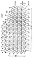
- Figure 2 shows the grouping of addend bits for an exemplary 16x16 multiplier/accumulator with nine partial products generated using encoding.
- Figures 3-8 taken together provide a schematic diagram of one embodiment of the triple array architecture corresponding to the multiplier/accumulator of Figure 2.
- Turning now to Figure 1, a triple array multiplier architecture will be described. The circuit includes a
multiplier input 10 and a multiplicand input 11. A multiplier signal atmultiplier input 10 is applied to anencoding circuit 12 and is converted to an encodedinput 13. Encoding may be performed according to several well known algorithms (e.g. a modified Booth's algorithm) so that the number of partial products generated from encodedinput 13 and multiplicand input 11 is less than would otherwise be generated. For example, using a modified Booth algorithm with a multiplier and multiplicand length of 16 bits each, encodedinput 13 is encoded into nine terms. As a result,partial product generator 14 would generate 9 partial products to be added to form the final product. -
Partial product generator 14 has as its output a plurality of partial products of increasing rank. The bits of the partial products are divided into groups which are summed in a triple adder array. SETA, one group of partial product bits, is input to the ADDA adder array. SETB, another group of partial products bits, is input to the ADDB adder array. A small number of remaining partial product bits SETCʹ can optionally be provided to the ADDC adder array. - In a preferred embodiment of the invention, SETA includes the bits of the r partial products of lowest order. The value of r is preferably greater than one-half n, where n is the total number of partial products. The results of the addition in the ADDA array include a low order portion of the final product, an intermediate sum SUMA and an intermediate carry CARA. The low order result is provided to a
register 15 and SUMA and CARA signals are input to the ADDC adder array. - Included in SETB are all or substantially all of the remaining partial product bits. The result of the addition in the ADDB array is SUMB, which is input to the ADDC adder array. There may be a small number of partial product bits which correspond to available adder locations in the ADDC array not being used to add SUMA, CARA and SUMB. These bits may be included in SETCʹ which bypasses the ADDA and ADDB arrays to be included in the ADDC array. The result of the addition in the ADDC adder array is the high order portion of the final result which is provided to register 15.
- According to the triple array architecture of the present invention, high speed and low complexity are achieved by implementing ADDA as a carry save array and ADDB and ADDC as carry look-ahead arrays. Thus, the ADDA array sums the low rank partial products while taking advantage of the low complexity and small chip area of a carry save array. The high speed of the carry look-ahead adder is advantageously employed in the ADDB and ADDC arrays in performing the higher rank summation. More specifically, the ADDA array preferably comprises r-1 rows of carry save adders for adding the partial products in SETA. ADDA may also comprise a row (i.e. a total of r rows) for handling accumulation and two's complement notation. ADDB and ADDC preferably each comprise one or more rows of carry save adders followed by a carry look-ahead adder.
- In another aspect of the preferred embodiment, the value of r is selected such that the time delay of carry save addition in ADDA is most closely equal to the time delay of carry look-ahead addition in ADDB. In this way, the architecture is optimized and SUMA, CARA and SUMB will be presented simultaneously to the ADDC array.
- The contents of
register 15 provide the output of the multiplier. In order to perform accumulation, the contents ofregister 15 may be fed back into the ADDA array for inclusion in subsequent processing. - In order to handle either signed or unsigned magnitude notation, the multiplicand (at input 11) is extended by two bits and the multiplier (at input 10) is extended by one bit. The value of the extended high order bits depends on the notation used and the value of the most significant bit of the original number. Thus, when signed notation is being used, the value of the most significant bit is repeated in each of the extra bits, e.g. a logical "1" in the MSB position of the multiplicand would be repeated in the two extension bits of input 11. When unsigned notation is being used, each of the extra bits is forced to a logical "0".
- In order to also handle two's complement signed notation,
partial product generator 14 may also include a two's complement register 16.Register 16 has a plurality of bits, each bit corresponding to a partial product. Each bit can be set in order to indicate that the corresponding partial product in two's complement notation is negative. When performing the addition of the partial products, the contents ofregister 16 must be added in. Preferably, each two's complement bit is added in the array which includes its respective partial product. - An example of a specific grouping of bits for a triple array multiplier adapted to perform 16 bit by 16 bit multiplication/accumulation using modified Booth algorithm encoding to generate 9 partial products is shown in Figure 2. The 9 partial products are designated P and P0 to P7. Each designation is followed by a bit designation 0 to H. P is the lowest order or least significant partial product. P7 is the highest order partial product. The least significant bits are designated 0 and the most significant bits by H. Figure 2 also shows the two's complement bits designated TC and TC0 to TC7. The contents of the accumulator register are designated OR0 to ORX2 and the two's complement bit for the accumulator register is shown as TCA.
- The bits in Figure 2 are arranged such that bits of equal significance are in the same vertical column. Thus, bit significant increases moving towards the right. Each two's complement bit has the same significance as the last significant bit of its respective partial product (or the accumulator register in the case of TCA).
- As shown in Figure 2, SETA includes the bits of 6 partial products, namely P and P0 to P4, the accumulator contents OR0 to ORX2 and the corresponding two's complement bits TC, TC0 to TC4 and TCA. SETB includes partial products P6 and P7 and corresponding two's complement bits TC6 and TC7, and includes bits P52 to P5H of partial product P5. Low order bits P50 and P51 and two's complement bit TC5 are grouped into SETCʹ.
- A triple array summation circuit for performing addition according to the groupings of Figure 2 is shown schematically in Figures 4 to 8 with Figure 3 showing how to arrange Figures 4 to 8.
- ADDA is a carry save array shown in Figures 4 to 6. The first row consists of half adders except in the sixteenth and nineteenth bit positions. A full adder is used in the sixteenth bit position to introduce a round bit RND to cause rounding off of the result when desired. A diamond adder is in the nineteenth bit position of the first row and has bit PG extended to its b input from the previous half adder. The input designations of the full adder, diamond adder and first half adder in the first row are repeated (but not shown) for the other adders of the same types in the figures.
- As is known in the art, a full adder (such as
full adder 40 in Figure 5) has addend inputs a and b, a carry input Cin, a sum output s and a carry output cout. A half adder, such as half adder 41, has a and b inputs and s and cout outputs. A diamond adder, such asdiamond adder 42, has a and b inputs, an s output and a "s or c" output which is the logical OR of the s and c outputs of a half adder. The bits input to each adder are as shown. Further, some inputs are hard wired to a logical "1" or a logical "0" as indicated. - The ADDA array also includes conditional sum adders MX0 to MX8. These are high speed adders which use a multiplexer to select one of two full adders according to its Cin input, as known in the art. The inverted low order bits of the final product are shown as
S0 toS10 in Figure 4. - ADDB comprises a row of full adders followed by a 20-bit carry look-ahead adder (CLA) 100, shown in Figures 7 and 8. The ADDC array comprises one row of full adders followed by a 24-
bit CLA 101. The inverted high order bits of the final product are output fromCLA 101 and are shown asS11 toS34 . In performing the final addition, the ADDC array receives an intermediate sum signal from the ADDB array and receives both an intermediate sum signal and an intermediate carry signal from the ADDA array. -
CLA 100 andCLA 101 are shown with their inputs at the top and outputs at the bottom. The CLAs can be of typical configuration as known in the art and shown, for example, in N. Scott, Computer Number Systems end Arithmetic (1985) and in US Patent No. 4,153,938, both of which are hereby incorporated by reference. - The foregoing triple array multiplier architecture with parallel summation by a carry save array and a first carry look-ahead array followed by final summation by a second carry look-ahead array achieves high speed, high performance and small chip area in a circuit which can be implemented with standard IC technology. The circuit is versatile, can perform accumulation and can operate with either signed or unsigned magnitude representation.
Claims (9)
- A multiplier circuit for producing the sum of a multiplier signal and a multiplicand signal comprising:
partial product generating means (13,14) for generating N addends, of different rank, each addend comprising a set of partial products comprised of an ordered set of bits, in response to a multiplier signal and a multiplicand signal applied to the inputs (10,11) of said partial product generating means;
a carry save array (ADDA) coupled to said partial product generating means for adding the bits of a first group of R addends taken from said N addends and for generating the least significant bits of said sum and generating intermediate sum and carry signals;
characterized by
a first carry look-ahead array (ADDB) operating in parallel and simultaneously with said carry save array coupled to said partial product generating means for adding substantially all of the bits of said N addends not included in said first group to generate an intermediate product; and
a second carry look-ahead array (ADDC) coupled to said carry save array and to said first carry look-ahead array, said second carry look-ahead array generating the most significant bits of said sum from said intermediate product and from said intermediate sum and carry signals; where N and R are integers with R being greater than one half of N - The multiplier circuit of claim 1 wherein said partial product generating means includes an encoding circuit (12) for encoding said multiplier signal to reduce the number of partial products which are generated.
- The multiplier circuit of claim 2 wherein said encoding circuit performs a modified Booth algorithm.
- The multiplier circuit of claim 1 further comprising an accumulator register (15) coupled to said carry save array and said second carry-look ahead array for receiving said sum, said carry save array adapted to add the contents of said accumulator register to said first group of bits in order to perform accumulation.
- The multiplier circuit of claim 1 further comprising a two's complement register (16) coupled to said carry save array and having a plurality of bits, each bit respectively indicating the sign of a respective partial product, the contents of said two's complement register being added into said sum.
- The multiplier circuit of claim 1 wherein said first group of R addends is further selected such that said intermediate sum and carry signals and said intermediate product are generated substantially simultaneously.
- the multiplier circuit of claim 1 wherein said partial product generating means generates nine addends, wherein said first group of addends added by said carry save array includes the bits of the six least significant addends, wherein said first carry look-ahead array comprises one row of full adders (P60 ....P69, P6A.....P6H) and a carry look-ahead adder (CLA100), and wherein said second carry look-ahead array comprises one row of full adders (P50,P51......) and a carry look-ahead adder (CLA101).
- A method for adding n partial products in a digital multiplier comprising the steps of:
adding the r least significant partial products of said n partial products in a carry save array (ADDA) to generate the least significant bits of the final sum and to generate intermediate sum and carry signals, said carry save array performing said addition in a time delay A; characterized by
simultaneously adding the bits of all the remaining partial products in a first carry look-ahead array (ADDB) to generate an intermediate product in a time delay B; and
adding said intermediate sum and carry signals and said intermediate products in a second carry look ahead array to generate the most significant bits of said final sum, the value of r being an integer greater than one half n. - The method of claim 8 wherein the value of r is selected to minimize the difference between time delay A and time delay B.
Applications Claiming Priority (2)
| Application Number | Priority Date | Filing Date | Title |
|---|---|---|---|
| US06/908,489 US4831577A (en) | 1986-09-17 | 1986-09-17 | Digital multiplier architecture with triple array summation of partial products |
| US908489 | 1986-09-17 |
Publications (3)
| Publication Number | Publication Date |
|---|---|
| EP0260515A2 EP0260515A2 (en) | 1988-03-23 |
| EP0260515A3 EP0260515A3 (en) | 1990-09-26 |
| EP0260515B1 true EP0260515B1 (en) | 1994-02-23 |
Family
ID=25425888
Family Applications (1)
| Application Number | Title | Priority Date | Filing Date |
|---|---|---|---|
| EP87112663A Expired - Lifetime EP0260515B1 (en) | 1986-09-17 | 1987-08-31 | Digital multiplier architecture with triple array summation of partial products |
Country Status (4)
| Country | Link |
|---|---|
| US (1) | US4831577A (en) |
| EP (1) | EP0260515B1 (en) |
| JP (1) | JPS6375932A (en) |
| DE (1) | DE3789132T2 (en) |
Families Citing this family (25)
| Publication number | Priority date | Publication date | Assignee | Title |
|---|---|---|---|---|
| US4839848A (en) * | 1987-09-14 | 1989-06-13 | Unisys Corporation | Fast multiplier circuit incorporating parallel arrays of two-bit and three-bit adders |
| US5278781A (en) * | 1987-11-12 | 1994-01-11 | Matsushita Electric Industrial Co., Ltd. | Digital signal processing system |
| US4972362A (en) * | 1988-06-17 | 1990-11-20 | Bipolar Integrated Technology, Inc. | Method and apparatus for implementing binary multiplication using booth type multiplication |
| JPH0776914B2 (en) * | 1988-10-18 | 1995-08-16 | 三菱電機株式会社 | Multiplication circuit |
| GB2226899A (en) * | 1989-01-06 | 1990-07-11 | Philips Electronic Associated | An electronic circuit and signal processing arrangements using it |
| US4969118A (en) * | 1989-01-13 | 1990-11-06 | International Business Machines Corporation | Floating point unit for calculating A=XY+Z having simultaneous multiply and add |
| EP0383965A1 (en) * | 1989-02-21 | 1990-08-29 | International Business Machines Corporation | Multiplier |
| JP2540934B2 (en) * | 1989-03-09 | 1996-10-09 | 三菱電機株式会社 | Logic circuit device |
| JPH07118630B2 (en) * | 1989-06-29 | 1995-12-18 | 三菱電機株式会社 | Signal processing circuit for multiplication |
| US5121352A (en) * | 1990-02-06 | 1992-06-09 | Micron Technology, Inc. | Multiplier-accumulator circuit array operable in multiple modes |
| US5121431A (en) * | 1990-07-02 | 1992-06-09 | Northern Telecom Limited | Processor method of multiplying large numbers |
| US5153850A (en) * | 1990-08-24 | 1992-10-06 | Mass Microsystems | Method and apparatus for modifying two's complement multiplier to perform unsigned magnitude multiplication |
| JPH04116720A (en) * | 1990-09-07 | 1992-04-17 | Hitachi Ltd | Semiconductor device |
| JP2838326B2 (en) * | 1991-04-16 | 1998-12-16 | 三菱電機株式会社 | Digital multiplier |
| US5218564A (en) * | 1991-06-07 | 1993-06-08 | National Semiconductor Corporation | Layout efficient 32-bit shifter/register with 16-bit interface |
| US5220525A (en) * | 1991-11-04 | 1993-06-15 | Motorola, Inc. | Recoded iterative multiplier |
| US5375078A (en) * | 1992-12-15 | 1994-12-20 | International Business Machines Corporation | Arithmetic unit for performing XY+B operation |
| KR0158647B1 (en) * | 1995-05-22 | 1998-12-15 | 윤종용 | Signed / unsigned multiplier |
| US5974437A (en) * | 1996-12-02 | 1999-10-26 | Synopsys, Inc. | Fast array multiplier |
| US6571268B1 (en) | 1998-10-06 | 2003-05-27 | Texas Instruments Incorporated | Multiplier accumulator circuits |
| US6523055B1 (en) | 1999-01-20 | 2003-02-18 | Lsi Logic Corporation | Circuit and method for multiplying and accumulating the sum of two products in a single cycle |
| US6215325B1 (en) | 1999-03-29 | 2001-04-10 | Synopsys, Inc. | Implementing a priority function using ripple chain logic |
| AU2003269332A1 (en) * | 2002-08-22 | 2004-03-11 | Med-El Elektromedizinische Gerate Gmbh | Method and system for multiplication of binary numbers |
| US20080225939A1 (en) * | 2007-03-15 | 2008-09-18 | Jiun-In Guo | Multifunctional video encoding circuit system |
| CN116414352A (en) * | 2021-12-31 | 2023-07-11 | 华为技术有限公司 | Circuits, Multiplier-Adders, and Circuit Optimization Methods |
Citations (1)
| Publication number | Priority date | Publication date | Assignee | Title |
|---|---|---|---|---|
| US3670956A (en) * | 1968-09-26 | 1972-06-20 | Hughes Aircraft Co | Digital binary multiplier employing sum of cross products technique |
Family Cites Families (16)
| Publication number | Priority date | Publication date | Assignee | Title |
|---|---|---|---|---|
| US3508038A (en) * | 1966-08-30 | 1970-04-21 | Ibm | Multiplying apparatus for performing division using successive approximate reciprocals of a divisor |
| US3675001A (en) * | 1970-12-10 | 1972-07-04 | Ibm | Fast adder for multi-number additions |
| US3866030A (en) * | 1974-04-01 | 1975-02-11 | Bell Telephone Labor Inc | Two{3 s complement parallel array multiplier |
| BE844199A (en) * | 1976-07-16 | 1976-11-16 | DEVICE FOR MULTIPLICATION OF BINARY NUMBERS | |
| US4153938A (en) * | 1977-08-18 | 1979-05-08 | Monolithic Memories Inc. | High speed combinatorial digital multiplier |
| US4215416A (en) * | 1978-03-22 | 1980-07-29 | Trw Inc. | Integrated multiplier-accumulator circuit with preloadable accumulator register |
| NL7809398A (en) * | 1978-09-15 | 1980-03-18 | Philips Nv | MULTIPLICATOR FOR BINARY NUMBERS IN TWO-COMPLEMENT NOTATION. |
| US4228520A (en) * | 1979-05-04 | 1980-10-14 | International Business Machines Corporation | High speed multiplier using carry-save/propagate pipeline with sparse carries |
| US4484301A (en) * | 1981-03-10 | 1984-11-20 | Sperry Corporation | Array multiplier operating in one's complement format |
| JPS593634A (en) * | 1982-06-30 | 1984-01-10 | Fujitsu Ltd | Multiplier |
| JPS5911445A (en) * | 1982-07-13 | 1984-01-21 | Nec Corp | Multiplier |
| US4545028A (en) * | 1982-10-13 | 1985-10-01 | Hewlett-Packard Company | Partial product accumulation in high performance multipliers |
| JPH0640301B2 (en) * | 1983-09-22 | 1994-05-25 | ソニー株式会社 | Parallel multiplier circuit |
| US4660165A (en) * | 1984-04-03 | 1987-04-21 | Trw Inc. | Pyramid carry adder circuit |
| US4575812A (en) * | 1984-05-31 | 1986-03-11 | Motorola, Inc. | X×Y Bit array multiplier/accumulator circuit |
| US4679164A (en) * | 1984-12-17 | 1987-07-07 | The United States Of America As Represented By The Secretary Of The Army | Digital high speed programmable convolver |
-
1986
- 1986-09-17 US US06/908,489 patent/US4831577A/en not_active Expired - Lifetime
-
1987
- 1987-08-24 JP JP62208402A patent/JPS6375932A/en active Granted
- 1987-08-31 EP EP87112663A patent/EP0260515B1/en not_active Expired - Lifetime
- 1987-08-31 DE DE3789132T patent/DE3789132T2/en not_active Expired - Fee Related
Patent Citations (1)
| Publication number | Priority date | Publication date | Assignee | Title |
|---|---|---|---|---|
| US3670956A (en) * | 1968-09-26 | 1972-06-20 | Hughes Aircraft Co | Digital binary multiplier employing sum of cross products technique |
Also Published As
| Publication number | Publication date |
|---|---|
| EP0260515A3 (en) | 1990-09-26 |
| JPH0543136B2 (en) | 1993-06-30 |
| DE3789132D1 (en) | 1994-03-31 |
| US4831577A (en) | 1989-05-16 |
| EP0260515A2 (en) | 1988-03-23 |
| DE3789132T2 (en) | 1994-10-13 |
| JPS6375932A (en) | 1988-04-06 |
Similar Documents
| Publication | Publication Date | Title |
|---|---|---|
| US4831577A (en) | Digital multiplier architecture with triple array summation of partial products | |
| US4168530A (en) | Multiplication circuit using column compression | |
| US5465226A (en) | High speed digital parallel multiplier | |
| US4839847A (en) | N-clock, n-bit-serial multiplier | |
| JP3244506B2 (en) | Small multiplier | |
| US3670956A (en) | Digital binary multiplier employing sum of cross products technique | |
| US3636334A (en) | Parallel adder with distributed control to add a plurality of binary numbers | |
| US5161119A (en) | Weighted-delay column adder and method of organizing same | |
| US4965762A (en) | Mixed size radix recoded multiplier | |
| US5343417A (en) | Fast multiplier | |
| US5497343A (en) | Reducing the number of carry-look-ahead adder stages in high-speed arithmetic units, structure and method | |
| EP0398568A2 (en) | Multiplier circuit | |
| US5944776A (en) | Fast carry-sum form booth encoder | |
| EP0109137B1 (en) | Partial product accumulation in high performance multipliers | |
| US5586071A (en) | Enhanced fast multiplier | |
| US5867415A (en) | Multiplication element including a wallace tree circuit having adders divided into high and low order adders | |
| US5257217A (en) | Area-efficient multiplier for use in an integrated circuit | |
| US5132921A (en) | High speed digital computing system | |
| US5999962A (en) | Divider which iteratively multiplies divisor and dividend by multipliers generated from the divisors to compute the intermediate divisors and quotients | |
| US5072419A (en) | Binary tree multiplier constructed of carry save adders having an area efficient floor plan | |
| EP0326414B1 (en) | High speed multiplier | |
| US5883825A (en) | Reduction of partial product arrays using pre-propagate set-up | |
| JPH056892B2 (en) | ||
| Scheunemann et al. | Optimizing Encoder and Decoder Blocks for a Power-Efficient Radix-4 Modified Booth Multiplier | |
| JPH0869372A (en) | Binary multiplier |
Legal Events
| Date | Code | Title | Description |
|---|---|---|---|
| PUAI | Public reference made under article 153(3) epc to a published international application that has entered the european phase |
Free format text: ORIGINAL CODE: 0009012 |
|
| AK | Designated contracting states |
Kind code of ref document: A2 Designated state(s): DE FR GB |
|
| RAP1 | Party data changed (applicant data changed or rights of an application transferred) |
Owner name: INTERSIL, INC. (A DELAWARE CORP.) |
|
| PUAL | Search report despatched |
Free format text: ORIGINAL CODE: 0009013 |
|
| AK | Designated contracting states |
Kind code of ref document: A3 Designated state(s): DE FR GB |
|
| 17P | Request for examination filed |
Effective date: 19901210 |
|
| 17Q | First examination report despatched |
Effective date: 19921002 |
|
| GRAA | (expected) grant |
Free format text: ORIGINAL CODE: 0009210 |
|
| AK | Designated contracting states |
Kind code of ref document: B1 Designated state(s): DE FR GB |
|
| REF | Corresponds to: |
Ref document number: 3789132 Country of ref document: DE Date of ref document: 19940331 |
|
| ET | Fr: translation filed | ||
| PLBE | No opposition filed within time limit |
Free format text: ORIGINAL CODE: 0009261 |
|
| STAA | Information on the status of an ep patent application or granted ep patent |
Free format text: STATUS: NO OPPOSITION FILED WITHIN TIME LIMIT |
|
| 26N | No opposition filed | ||
| PGFP | Annual fee paid to national office [announced via postgrant information from national office to epo] |
Ref country code: FR Payment date: 19960715 Year of fee payment: 10 |
|
| PGFP | Annual fee paid to national office [announced via postgrant information from national office to epo] |
Ref country code: DE Payment date: 19960716 Year of fee payment: 10 |
|
| PGFP | Annual fee paid to national office [announced via postgrant information from national office to epo] |
Ref country code: GB Payment date: 19960724 Year of fee payment: 10 |
|
| PG25 | Lapsed in a contracting state [announced via postgrant information from national office to epo] |
Ref country code: GB Free format text: LAPSE BECAUSE OF NON-PAYMENT OF DUE FEES Effective date: 19970831 |
|
| GBPC | Gb: european patent ceased through non-payment of renewal fee |
Effective date: 19970831 |
|
| PG25 | Lapsed in a contracting state [announced via postgrant information from national office to epo] |
Ref country code: FR Free format text: LAPSE BECAUSE OF NON-PAYMENT OF DUE FEES Effective date: 19980430 |
|
| PG25 | Lapsed in a contracting state [announced via postgrant information from national office to epo] |
Ref country code: DE Free format text: LAPSE BECAUSE OF NON-PAYMENT OF DUE FEES Effective date: 19980501 |
|
| REG | Reference to a national code |
Ref country code: FR Ref legal event code: ST |