EP0254691B1 - Method and apparatus for testing eprom type semiconductor devices during burn-in - Google Patents
Method and apparatus for testing eprom type semiconductor devices during burn-in Download PDFInfo
- Publication number
- EP0254691B1 EP0254691B1 EP87830271A EP87830271A EP0254691B1 EP 0254691 B1 EP0254691 B1 EP 0254691B1 EP 87830271 A EP87830271 A EP 87830271A EP 87830271 A EP87830271 A EP 87830271A EP 0254691 B1 EP0254691 B1 EP 0254691B1
- Authority
- EP
- European Patent Office
- Prior art keywords
- devices
- cards
- burn
- chamber
- slots
- Prior art date
- Legal status (The legal status is an assumption and is not a legal conclusion. Google has not performed a legal analysis and makes no representation as to the accuracy of the status listed.)
- Expired - Lifetime
Links
- 238000012360 testing method Methods 0.000 title claims description 61
- 238000000034 method Methods 0.000 title claims description 15
- 239000004065 semiconductor Substances 0.000 title claims description 8
- 230000006870 function Effects 0.000 claims description 12
- 230000015654 memory Effects 0.000 claims description 11
- 238000012795 verification Methods 0.000 claims description 8
- 238000010438 heat treatment Methods 0.000 claims description 7
- 238000003780 insertion Methods 0.000 claims description 6
- 230000037431 insertion Effects 0.000 claims description 6
- 230000008878 coupling Effects 0.000 claims description 5
- 238000010168 coupling process Methods 0.000 claims description 5
- 238000005859 coupling reaction Methods 0.000 claims description 5
- 238000012545 processing Methods 0.000 claims description 5
- 239000011810 insulating material Substances 0.000 claims description 3
- 230000014759 maintenance of location Effects 0.000 claims description 3
- 238000004519 manufacturing process Methods 0.000 description 8
- 230000008569 process Effects 0.000 description 6
- 238000011990 functional testing Methods 0.000 description 4
- 230000000694 effects Effects 0.000 description 3
- 238000007667 floating Methods 0.000 description 3
- 230000005855 radiation Effects 0.000 description 2
- 206010053615 Thermal burn Diseases 0.000 description 1
- 230000009471 action Effects 0.000 description 1
- 230000015556 catabolic process Effects 0.000 description 1
- 230000007547 defect Effects 0.000 description 1
- 238000006731 degradation reaction Methods 0.000 description 1
- 238000010586 diagram Methods 0.000 description 1
- 238000005516 engineering process Methods 0.000 description 1
- 238000002347 injection Methods 0.000 description 1
- 239000007924 injection Substances 0.000 description 1
- 238000009413 insulation Methods 0.000 description 1
- 239000002184 metal Substances 0.000 description 1
- 238000004377 microelectronic Methods 0.000 description 1
- 238000012544 monitoring process Methods 0.000 description 1
- 238000005036 potential barrier Methods 0.000 description 1
- 238000003908 quality control method Methods 0.000 description 1
- 238000005215 recombination Methods 0.000 description 1
- 230000006798 recombination Effects 0.000 description 1
- 230000008672 reprogramming Effects 0.000 description 1
- 238000012552 review Methods 0.000 description 1
- 230000004936 stimulating effect Effects 0.000 description 1
- 238000012546 transfer Methods 0.000 description 1
Images


Classifications
-
- G—PHYSICS
- G01—MEASURING; TESTING
- G01R—MEASURING ELECTRIC VARIABLES; MEASURING MAGNETIC VARIABLES
- G01R31/00—Arrangements for testing electric properties; Arrangements for locating electric faults; Arrangements for electrical testing characterised by what is being tested not provided for elsewhere
- G01R31/28—Testing of electronic circuits, e.g. by signal tracer
- G01R31/2851—Testing of integrated circuits [IC]
- G01R31/2855—Environmental, reliability or burn-in testing
- G01R31/286—External aspects, e.g. related to chambers, contacting devices or handlers
- G01R31/2868—Complete testing stations; systems; procedures; software aspects
-
- G—PHYSICS
- G01—MEASURING; TESTING
- G01R—MEASURING ELECTRIC VARIABLES; MEASURING MAGNETIC VARIABLES
- G01R31/00—Arrangements for testing electric properties; Arrangements for locating electric faults; Arrangements for electrical testing characterised by what is being tested not provided for elsewhere
- G01R31/26—Testing of individual semiconductor devices
- G01R31/2642—Testing semiconductor operation lifetime or reliability, e.g. by accelerated life tests
-
- G—PHYSICS
- G11—INFORMATION STORAGE
- G11C—STATIC STORES
- G11C29/00—Checking stores for correct operation ; Subsequent repair; Testing stores during standby or offline operation
- G11C29/04—Detection or location of defective memory elements, e.g. cell constructio details, timing of test signals
- G11C29/50—Marginal testing, e.g. race, voltage or current testing
-
- G—PHYSICS
- G11—INFORMATION STORAGE
- G11C—STATIC STORES
- G11C29/00—Checking stores for correct operation ; Subsequent repair; Testing stores during standby or offline operation
- G11C29/04—Detection or location of defective memory elements, e.g. cell constructio details, timing of test signals
- G11C29/50—Marginal testing, e.g. race, voltage or current testing
- G11C29/50012—Marginal testing, e.g. race, voltage or current testing of timing
-
- G—PHYSICS
- G11—INFORMATION STORAGE
- G11C—STATIC STORES
- G11C29/00—Checking stores for correct operation ; Subsequent repair; Testing stores during standby or offline operation
- G11C29/04—Detection or location of defective memory elements, e.g. cell constructio details, timing of test signals
- G11C29/50—Marginal testing, e.g. race, voltage or current testing
- G11C29/50016—Marginal testing, e.g. race, voltage or current testing of retention
-
- G—PHYSICS
- G11—INFORMATION STORAGE
- G11C—STATIC STORES
- G11C16/00—Erasable programmable read-only memories
- G11C16/02—Erasable programmable read-only memories electrically programmable
- G11C16/04—Erasable programmable read-only memories electrically programmable using variable threshold transistors, e.g. FAMOS
Definitions
- the present invention generally relates to the production techniques of integrated circuits and, more particularly, to the quality control procedures which, inserted as they are in the manufacturing flow, may be considered under many aspects an integral part of the production process itself.
- the present invention concerns, in fact, an apparatus and a method for testing the functions and parametric characteristics of integrated circuits, particularly of integrated circuits containing sections of read-only type EPROM memory (acronym of Erasable Programmable Read-Only Memory).
- the quality and reliability of semiconductor devices are based, besides on the technology employed in the fabrication process, on a series of tests to which the product is subjected before being delivered to the user.
- the time required to run an N2 test pattern on a typical 16K RAM is of about a minute; for a 64K RAM, it increases to about 30 minutes; and for a 256K RAM, it becomes of 8 hours.
- Such test times are, on the other hand, easily accomodated in the times necessary to effect the burn-in treatment.
- Test programs must be under the control of a central processing unit (CPU) that is capable of monitoring inputs and outputs of the devices under test to verify the validity of the tests.
- CPU central processing unit
- the working temperature is, in fact, directly responsible of the recombination or loss of electrical charges stored in the permanent memory element represented by a "floating gate” structure, which is the site of the data programmed in the device by injection of a certain electrical charge in such a floating structure, i.e. completely insulated from the rest of the circuit.
- EPROM devices in contrast with other devices such as microprocessors and random access memories (RAM), show another peculiarity typical of their function: they must be programmed with a specific content and then checked for their function. Thereafter in order to confirm their function with a different content, the same devices must be erased by exposure to a U.V. (ultraviolet) radiation for about 10-15 minutes.
- U.V. ultraviolet
- GB-A- 2 168 802 discloses a burn-in tester using cards for mounting the devices under test, the cards comprising a test control logic. Of each card, only the part having the devices under test mounted thereon is inserted into the heating chamber while the part comprising test control logic remains outside This known burn-in tester does not provide means for erasing EPROMS in the heating chamber by irradiation of UV light.
- DC parametric
- TAC access time
- Fig. 1 shows the general architecture of the system of the invention.
- Fig. 1 two substantially identical distinct systems, generally indicated with 1 and 2, are shown.
- Each distinct system has a proper console 4, associated with a CPU, and which is provided with a key board 5 and monitor 6.
- Each system comprises one or more ovens 3, provided with heating means and with means for controlling the temperature inside the chamber of the oven, preferably under control of the CPU.
- the windows present on the front wall of the ovens 3, shown in Fig. 1, are indicated with 9, while the windows present on the back wall of the ovens are indicated with 10.
- Such windows or slots 9 and 10 permit the insertion inside the oven 3 of an equal number of cards 7 and 8.
- Fig. 3 shows the configuration of each of said windows 9 or 10.
- Each window or slot is defined through the insulating wall of the oven 13 by a frame 11 fitted in a suitable opening cut through said wall 13 and having an aperture or central port of substantially rectangular section which extends through the thickness of said frame in a tapering way to form a slot having a truncated pyramid passage whose major base corresponds with the external surface 14 of the oven and whose minor base corresponds with the internal surface 15 of the oven chamber wall.
- each individual slot may be advantageously formed by two pairs of flaps, 12a and 12b, suitably hinged and provided with elastic return means (e.g. springs) as to automatically close when a card is not inserted through the slot.
- elastic return means e.g. springs
- Naturally other automatic means for closing the aperture of the slots in absence of cards inserted through the same may be devised and utilized for the purpose.
- the frame 11 is made with a heat insulating material to avoid constituting a heat bridge between the internal chamber of the oven and the room environment.
- a card 7 comprises two parts or sections; a first part 16 is provided, on a face thereof, with a plurality of parallel connected sockets into which an equal number of EPROM devices, 17, to be subjected to burn-in and to be tested may be plugged, and a second part or section 18 containing a microprocessor typically formed by a central processing unit, a read-only memory, a random access memory, as well as input and output interfacing stages (CPU, ROM, RAM, I/O).
- the two parts 16 and 18 are separated by a central body 19, shaped as a truncated pyramid with rectangular base, matching with the central opening of the frame 11 of said windows 9.
- Such a central coupling body 19 will be also preferably made of insulating material.
- the card may be provided with a handle 20 for improving handling thereof.
- Means, not shown, for connecting the card's microprocessor to the system's CPU as well as to the power supply are also contemplated within the portion 18 of each card.
- This second type of cards comprises a frame 21 capable of accommodating one or, preferably, more U.V. lamps 22 functionally mounted in appropriate sockets fixed to the frame 21.
- this second type of cards 8 may be conveniently provided with a handle 20 .
- the relative arrangement of the two types of cards inside the oven's chamber is such that each card 8 carrying the U.V. lamps is inserted between a pair of devices carrying cards 7 which are mounted so as to ensure that the devices 17, arranged on one of the two sides of each of the pair of cards, be opposing the U.V. lamps 22 mounted on the card 8.
- the devices cards 7 are mounted through the slots of the front wall 13 of the ovens, while the U.V. lamp cards 8 are suitably inserted through slots of the back wall 13 ⁇ of the ovens.
- the portion 18 of the devices cards 7 containing the microprocessors and the portion 23 of the U.V. lamps cards 8, containing the switching means for the lamps, remain outside the hot chamber of the oven.
- the microprocessor contained in the external portion 18 of the devices cards 7 executes, among others, the following functions:
- the system's CPU provides also to send the switch-on and switch-off signals for the U.V. lamps mounted on the various cards 8 for carrying out the erasing operations of the data programmed into the EPROM devices being tested during specific phases of the entire burn-in cycle and of the functional testing and of the determination of the parametric characteristics of the devices.
- the system's CPU performs a general supervisory function of the system determining the contemplated test sequence during the burn-in heat treatment.
- the CPU records and processes data generated by the testing and it is capable of directing the "intelligent" unloading of the EPROM devices from the test cards at the end of the cycle, by guiding the action of an unloading "robot” which will unplug one by one the devices from each card, placing each device in a classified container or tube in function of the detected and recorded performances of each individual device.
- FIG. 7 A presently preferred flow chart of the process of the invention is shown in Fig. 7. Such a flow chart may be considered indicative of a backend production flow of EPROM type semiconductor devices.
- the single devices whose memory cells have been all programmed to "0", coming directly from the assembly lines without having been through any quality test, are loaded in metal tubes (usually aluminun tubes) and placed in an oven at 170°C for 72 hours.
- the tubes containing the devices are then moved to an automatic machine for loading the devices on the special burn-in cards of the system of the invention.
- the loading robot provides to plug the devices in the sockets of the card and, upon plugging, the card microprocessor verifies the presence or absence of short circuits at the outputs of the devices; in an affermative case, the device is immediately unplugged from the socket and placed among rejects.
- Each card, completely loaded with devices, is introduced into the burn-in oven and connected to the system's CPU.
- the devices loaded on to the cards are then subjected to a dynamic burn-in treatment at 125°C for 24 hours during which time the devices undergo the following tests:
- the cards containing the devices are moved to an automatic machine or robot which provides to unplug the devices from the sockets of the cards and, in function of the grade or classification attributed to the device (depending upon the results of the tests to which the device has been subjected) which has been memorized by the card microprocessor, to deposite the single devices into relative classified tubes.
- Different lots of devices already classified in function of their shown performances in respect of the parametric testing and functional testing may be fed to an automatic testing apparatus for the determination of the access time (TAC) and for the relative further classification of the devices into quality grades.
- TAC access time
- the devices are then stamped and erased.
- the devices may be considered ready for shipment although a further checking of the erasure of the test data and/or an eventual second access time test may also be contemplated.
- the described sequence may, of course, be made completely automatic by providing suitable transfer means for the cards and for the tubes.
- the apparatus object of the present invention permits of essentially combining the burn-in test with functional and parametric testing of the EPROM devices, thus reducing in a large measure the test times and the handling of the devices besides permitting to perform the parametric and functional tests of the EPROM devices while they are being subjected to the burn-in treatment, thus ensuring a higher degree of reliability of the product.
Landscapes
- Engineering & Computer Science (AREA)
- General Physics & Mathematics (AREA)
- Physics & Mathematics (AREA)
- Microelectronics & Electronic Packaging (AREA)
- General Engineering & Computer Science (AREA)
- Computer Hardware Design (AREA)
- Environmental & Geological Engineering (AREA)
- Tests Of Electronic Circuits (AREA)
- Testing Of Individual Semiconductor Devices (AREA)
- Semiconductor Memories (AREA)
- Non-Volatile Memory (AREA)
- For Increasing The Reliability Of Semiconductor Memories (AREA)
- Testing Or Measuring Of Semiconductors Or The Like (AREA)
Description
- The present invention generally relates to the production techniques of integrated circuits and, more particularly, to the quality control procedures which, inserted as they are in the manufacturing flow, may be considered under many aspects an integral part of the production process itself.
- The present invention concerns, in fact, an apparatus and a method for testing the functions and parametric characteristics of integrated circuits, particularly of integrated circuits containing sections of read-only type EPROM memory (acronym of Erasable Programmable Read-Only Memory).
- The quality and reliability of semiconductor devices are based, besides on the technology employed in the fabrication process, on a series of tests to which the product is subjected before being delivered to the user.
- One of the tests regarded as one of the most severe is that of subjecting the devices to particularly high temperatures; typically between 85°C and 150°C, for accelarating infant mortalities in a population of semiconductor devices. This test, also known among the experts of the field as "burn-in" has the objective of provoking or otherwise stimulating the failure of those devices which have developed some defects during the fabrication process and/or during handling and whose structure thus contains some elemens of precariousness.
- Since the burn-in treatment requires that thousands of devices be plugged into parallel sockets mounted on appropriate cards suitable to be inserted in a heat treatment chamber for a considerable number of hours, becomes economically desirable to be able to perform a series of functional tests of the devices during their "captivity" into the burn-in chamber. This demand has intensified as memories and logic devices have become increasingly dense and complex, thus requiring increasingly longer test times.
- For example, the time required to run an N² test pattern on a typical 16K RAM, is of about a minute; for a 64K RAM, it increases to about 30 minutes; and for a 256K RAM, it becomes of 8 hours. Such test times are, on the other hand, easily accomodated in the times necessary to effect the burn-in treatment.
- Adequate functional testing during burn-in requires sophisticated pattern-generation and advanced control and data-processing capabilities. Test programs must be under the control of a central processing unit (CPU) that is capable of monitoring inputs and outputs of the devices under test to verify the validity of the tests.
- The possibility of effecting functional tests while the devices are kept at high temperatures, becomes particularly important in the case of EPROM type devices. The working temperature is, in fact, directly responsible of the recombination or loss of electrical charges stored in the permanent memory element represented by a "floating gate" structure, which is the site of the data programmed in the device by injection of a certain electrical charge in such a floating structure, i.e. completely insulated from the rest of the circuit.
- The higher the temperature, the higher the probability that electrical charges stored in the floating gate acquire sufficient energy to overcome the potential barrier represented by the insulation thus disappearing from their assigned site and thus modifying the information stored therein.
- Moreover, EPROM devices, in contrast with other devices such as microprocessors and random access memories (RAM), show another peculiarity typical of their function: they must be programmed with a specific content and then checked for their function. Thereafter in order to confirm their function with a different content, the same devices must be erased by exposure to a U.V. (ultraviolet) radiation for about 10-15 minutes.
- The article entitled: "New Testing Strategy: Test During Burn-In" by Carl N. Buck, Microelectronics Manufacturing and Testing, November 1985, Page 57 and 58, provides a review of the technique of performing back-end testing of semiconductor devices during a burn-in treatment, for various categories of devices, namely SRAMs, DRAMs and EPROMs. Notwithstanding the attempts to streamline and reduce handling during a back-end testing process for EPROMs, the burden remains of repeatedly moving the test cards onto which the devices are mounted to an erase station before reprogramming a different test pattern to be tested during a burn-in treatment.
- GB-A- 2 168 802 discloses a burn-in tester using cards for mounting the devices under test, the cards comprising a test control logic. Of each card, only the part having the devices under test mounted thereon is inserted into the heating chamber while the part comprising test control logic remains outside This known burn-in tester does not provide means for erasing EPROMS in the heating chamber by irradiation of UV light.
- This erasing operation is of great encumbrance in the flow relative to the last steps of the production process which includes the burn-in treatment too. According to prior art methods, it is necessary to remove from the burn-in chamber the devices for subjecting them to U.V. radiation and thence to replug them into the sockets of the cards to be reinserted into the burn-in chambers. Because of these difficulties, it is usually preferred to effect the burn-in test with a single content of the devices (i.e. with a single test pattern programmed into the devices) with an evident degradation of the qualitative objectives of the test itself.
- It is the object of the present invention to overcome completely the above noted problems and to permit to effect an entire series of functional tests for checking the content of the appropriately programmed memory cells, of tests to establish the parametric (DC) characteristics of the devices, of dynamic tests to verify the access time (TAC) and of recording the classification for a subsequent marking of the devices, during the time they remain inside the burn-in chamber, thus efficiently integrating such tests with the thermal burn-in treatment itself.
- This object is achieved with an apparatus according to
Claim 1 and with a process according toClaim 7. - The invention, its different aspects and advantages will be more easily understood through the following description, having a purely illustrative and nonlimitative character, of a preferred embodiment of the invention illustrated also by a series of annexed drawings, wherein
- Figure 1 is a perspective view of two integrated burn-in, functional testing, AC and DC parametric testing systems for EPROM type semiconductor devices in accordance with the present invention;
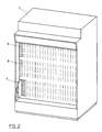
- Figure 2 is an enlarged view of the front portion of one of the ovens or heat treatment chambers used in the system of the invention;
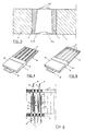
- Figure 3 is a partial sectional view of one of the "windows" or slots for inserting cards containing the devices to be tested present on front and back walls of the ovens;
- Figure 4 is a schematic, perspective view of one of the system's cards;
- Figure 5 is a schematic, perspective view of one of the cards containing U.V. lamps used in the system of the invention;
- Figure 6 is a partial, schematic, sectional, plan view of one of the ovens used in the system of the invention, showing the arrangment of the different cards inside the oven;
- Figure 7 shows a functional flow diagram of the method of the invention.
- Fig. 1 shows the general architecture of the system of the invention. In Fig. 1 two substantially identical distinct systems, generally indicated with 1 and 2, are shown. Each distinct system has a proper console 4, associated with a CPU, and which is provided with a
key board 5 andmonitor 6. Each system comprises one ormore ovens 3, provided with heating means and with means for controlling the temperature inside the chamber of the oven, preferably under control of the CPU. On at least a wall and more preferably on two opposite walls of each oven, there is a series of "windows" (or slots), individually provided with closing means. The windows present on the front wall of theovens 3, shown in Fig. 1, are indicated with 9, while the windows present on the back wall of the ovens are indicated with 10. Such windows orslots oven 3 of an equal number ofcards - The enlarged showing of a
single oven 3 in Fig. 2 permits to observe, in greater detail, the arrangement ofsuch windows 9 on the front side of theoven 3 as well as of acard 7, inserted into one of such slots. - Fig. 3 shows the configuration of each of said
windows oven 13 by aframe 11 fitted in a suitable opening cut throughsaid wall 13 and having an aperture or central port of substantially rectangular section which extends through the thickness of said frame in a tapering way to form a slot having a truncated pyramid passage whose major base corresponds with theexternal surface 14 of the oven and whose minor base corresponds with the internal surface 15 of the oven chamber wall. - The closing means of each individual slot may be advantageously formed by two pairs of flaps, 12a and 12b, suitably hinged and provided with elastic return means (e.g. springs) as to automatically close when a card is not inserted through the slot. Naturally other automatic means for closing the aperture of the slots in absence of cards inserted through the same may be devised and utilized for the purpose.
- Preferably the
frame 11 is made with a heat insulating material to avoid constituting a heat bridge between the internal chamber of the oven and the room environment. - The system utilizes a plurality of
cards 7 having the configuration shown in Fig. 4. Acard 7 comprises two parts or sections; afirst part 16 is provided, on a face thereof, with a plurality of parallel connected sockets into which an equal number of EPROM devices, 17, to be subjected to burn-in and to be tested may be plugged, and a second part orsection 18 containing a microprocessor typically formed by a central processing unit, a read-only memory, a random access memory, as well as input and output interfacing stages (CPU, ROM, RAM, I/O). The twoparts central body 19, shaped as a truncated pyramid with rectangular base, matching with the central opening of theframe 11 of saidwindows 9. Such acentral coupling body 19 will be also preferably made of insulating material. - The card may be provided with a
handle 20 for improving handling thereof. - Means, not shown, for connecting the card's microprocessor to the system's CPU as well as to the power supply are also contemplated within the
portion 18 of each card. - The configuration of the second type of cards utilized by the apparatus of the present invention is shown in Fig. 5. This second type of cards comprises a
frame 21 capable of accommodating one or, preferably, more U.V.lamps 22 functionally mounted in appropriate sockets fixed to theframe 21. Acentral body 19, having a truncated pyramid shape similar to that of the system's card described in Fig. 4, provides coupling means with the opening of saidwindows 10 in the wall of the oven. In thepart 23 of the card which remains outside of the oven chamber when the card is inserted into one of the slots, there are supply and switching means for the U.V.lamps 22 as well as means for the electric interconnection to the rest of the system's circuit. Also this second type ofcards 8 may be conveniently provided with ahandle 20 . - The relative arrangement into the oven of the two types of cards, i.e. of the
devices carrying cards 7 and of the U.V.lamps cards 8, is shown in Fig. 6. - Essentially, the relative arrangement of the two types of cards inside the oven's chamber is such that each
card 8 carrying the U.V. lamps is inserted between a pair ofdevices carrying cards 7 which are mounted so as to ensure that thedevices 17, arranged on one of the two sides of each of the pair of cards, be opposing the U.V.lamps 22 mounted on thecard 8. Preferably, thedevices cards 7 are mounted through the slots of thefront wall 13 of the ovens, while the U.V.lamp cards 8 are suitably inserted through slots of the back wall 13ʹ of the ovens. - As it may be easily observed in the schematic showing of Fig. 6, upon insertion, the
portion 18 of thedevices cards 7 containing the microprocessors and theportion 23 of the U.V.lamps cards 8, containing the switching means for the lamps, remain outside the hot chamber of the oven. - The microprocessor contained in the
external portion 18 of thedevices cards 7 executes, among others, the following functions: - A) suitably elaborates the signals sent to the EPROM devices being tested mounted on the card as to perform the programming and verification functions of the data content by performing pre-established different test patterns; classifies the devices into quality categories in function of the checked performances and detects rejects;
- B) interfaces with the system's CPU, receiving from the latter supervisory commands relative to the operations to be performed on the EPROM devices, communicates back to the system's CPU the results of these operations; these information will be stored by the CPU for subsequently governing the "intelligent" unloading of the devices from the burn-in cards.
- The system's CPU provides also to send the switch-on and switch-off signals for the U.V. lamps mounted on the
various cards 8 for carrying out the erasing operations of the data programmed into the EPROM devices being tested during specific phases of the entire burn-in cycle and of the functional testing and of the determination of the parametric characteristics of the devices. - Therefore, the system's CPU performs a general supervisory function of the system determining the contemplated test sequence during the burn-in heat treatment. The CPU records and processes data generated by the testing and it is capable of directing the "intelligent" unloading of the EPROM devices from the test cards at the end of the cycle, by guiding the action of an unloading "robot" which will unplug one by one the devices from each card, placing each device in a classified container or tube in function of the detected and recorded performances of each individual device.
- Such procedures for the classification of EPROM devices in accordance with their quality, as well as such means and procedures for the automation of handling and selection of the devices are well known to the expert technician of the field and therefore, in order not to unduly burden the present specification, will not be described, referring the reader to the vast and easily accessible literature on this particular topic.
- A presently preferred flow chart of the process of the invention is shown in Fig. 7. Such a flow chart may be considered indicative of a backend production flow of EPROM type semiconductor devices.
- The single devices whose memory cells have been all programmed to "0", coming directly from the assembly lines without having been through any quality test, are loaded in metal tubes (usually aluminun tubes) and placed in an oven at 170°C for 72 hours.
- The tubes containing the devices are then moved to an automatic machine for loading the devices on the special burn-in cards of the system of the invention. The loading robot provides to plug the devices in the sockets of the card and, upon plugging, the card microprocessor verifies the presence or absence of short circuits at the outputs of the devices; in an affermative case, the device is immediately unplugged from the socket and placed among rejects.
- Each card, completely loaded with devices, is introduced into the burn-in oven and connected to the system's CPU.
- The devices loaded on to the cards are then subjected to a dynamic burn-in treatment at 125°C for 24 hours during which time the devices undergo the following tests:
- i) verification of state "0" retention by all EPROM cells;
- ii) erasure;
- iii) programming of a first test pattern;
- iv) verification of the first test pattern;
- v) repetition of steps ii), iii) and iv) for a "n" number of different test patterns;
- vi) programming of a special checker-board pattern in order to prepare the EPROM devices for the subsequent dynamic testing for determining the access time (TAC).
- The cards containing the devices are moved to an automatic machine or robot which provides to unplug the devices from the sockets of the cards and, in function of the grade or classification attributed to the device (depending upon the results of the tests to which the device has been subjected) which has been memorized by the card microprocessor, to deposite the single devices into relative classified tubes.
- Different lots of devices already classified in function of their shown performances in respect of the parametric testing and functional testing may be fed to an automatic testing apparatus for the determination of the access time (TAC) and for the relative further classification of the devices into quality grades.
- The devices are then stamped and erased.
- At this point the devices may be considered ready for shipment although a further checking of the erasure of the test data and/or an eventual second access time test may also be contemplated.
- The described sequence may, of course, be made completely automatic by providing suitable transfer means for the cards and for the tubes.
- The type, the number and the re-iteration of the various tests, as well as the residence times and the test temperatures may be also different from those indicated in order to satisfy particular requirements. In all cases the apparatus object of the present invention permits of essentially combining the burn-in test with functional and parametric testing of the EPROM devices, thus reducing in a large measure the test times and the handling of the devices besides permitting to perform the parametric and functional tests of the EPROM devices while they are being subjected to the burn-in treatment, thus ensuring a higher degree of reliability of the product.
Claims (7)
- An apparatus for functional testing and for determining the characteristics of EPROM type semiconductor devices during a burn-in heat treatment, comprising means for erasing the EPROM devices by U.V. light irradiation, means for programming the EPROMs, means for verifying the programming of the EPROMs, means for performing the burn-in of the programmed devices, means for verifying the retention of the programmed data, means for measuring parametric (DC) and dynamic (TAC) characteristics of the devices and means for classifying and handling the single devices, which comprises:a) at least a burn-in chamber (3) provided, on at least a wall thereof, with a plurality of slots (9, 10) having automatic closing means (12a, 12b) and capable of receiving a card (7, 8);b) a plurality of first cards (7) for mounting the devices (17) to be tested, each of said first cards comprising a first part (16) provided with a plurality of parallely connected sockets for plugging in the devices (17) and a second part (18) containing a microprocessor, a coupling body (19) fitting into said slots being present between said first part (16) and second part (18) of each of said first cards (7), said second part (18) of said first cards (7) remaining outside said chamber (3) upon insertion of the card into one of said slots (9);c) a plurality of second cards (8) containing at least one U.V. lamp (22), each of said second cards comprising a first part (21) provided with at least one U.V. lamp (22) and a second part (23) containing switching and supply means for said lamp, a coupling body (19) suitably fitting into said slots (10) being present between said two parts (21, 23) of each one of said second cards (8), the second part (23) of each of said second cards (8) remaining outside said chamber (3) upon insertion of the card (8) into one of said slots (10);d) a system's central processing unit (CPU) (4) interfaced with the microprocessor of each of said first cards (7) for mounting the devices to be tested and with the switching means of each of said second cards (8) containing at least a U.V. lamp (22);each of said U.V. lamps containing second cards (8) being functionally interposed between two of said first cards (7) for mounting the devices to be tested;
said microprocessors determining the performance of the following operations upon the devices: programming, verification of the programming, verification of retention of programmed data, classification of devices in terms of quality and identification of the devices under control of the system's central processing unit which coordinates the switching of said U.V. lamps for erasing operations. - The apparatus according to claim 1, wherein said slots (9, 10) for inserting said first and second cards (7, 8) are defined through a wall (13) of said burn-in chamber (3) by a frame (11) of insulating material having a central opening (9, 10) with a substantially rectangular cross section and tapered across the thickness of the wall (13) of the chamber (3) to form a truncated pyramid port having a rectangular base and with the major base of the truncated pyramid corresponding with the external surface (14) of said wall (13).
- The apparatus according to claim 2, wherein said slots (9, 10) are provided with individual automatic means (12a, 12b) for closing the slot in absence of a card inserted into the slot itself.
- The apparatus according to claim 1, wherein said first and second cards (7, 8) are provided with a central coupling body (19) shaped as a truncated pyramid plug and matching with the shape of the opening of said slots (9, 10).
- The apparatus according to claim 1, wherein said microprocessor housed in said second part (18) of said first cards (7) for mounting the devices (17) to be tested remaining outside the burn-in chamber (3) upon insertion of the card (7) into one of said slots (9), comprises a control unit, a read-only memory, a ramdom access memory and input and output interfacing stages.
- The apparatus according to claim 1, wherein said first cards (7) for mounting the devices (17) are inserted inside the burn-in chamber (3) through the slots (9) of a front wall (13) of said chamber (3) and said second cards (8) carrying U.V. lamps (22) are inserted inside the burn-in chamber (3) through the slots (10) of a back wall (13') of said chamber (3).
- A method for functional testing and for determining the characteristics of EPROM type semiconductor devices during a burn-in treatment comprising the following steps:A) programming an "all 0" pattern the cells of the EPROM devices as received from the assembly lines;B) loading of the devices into tubes and storing at a temperature equal to or greater than 170°C for at least 72 hours;C) automatic loading of single devices from said tubes on cards provided with suitable sockets; verification of the validity of the data programmed during step A) and automatic rejection of nonvalidated devices;D) dynamic burn-in treatment at a temperature equal to or greater than 125°C carried out in a burn-in chamber and subjecting the devices plugged into said sockets of said cards to the following tests under the control of a card microprocessor without removing said cards from said burn-in chamber:i) verification of the "0" status of all the EPROM cells;ii)erasing by means of U.V. lamp carrying cards intermeshed with said device carrying cards inside said burn-in chamber;iii) programming of a test pattern;iv) verification of the test pattern;v) repetition of steps ii), iii) and iv) for an "n" number of different test patterns;vi) classification of the single devices according to particular quality classes;vii) programming of a special pattern for subsequent testing;E) automatic unplugging of the devices from the sockets of said cards and their classification by automatic insertion of the devices into classified tubes in accordance with particular quality grades;F) testing of dynamic (TAC) parameters of the devices and further classification of devices in function of the determined individual dynamic characteristics;G) stamping of the devices and final erasing of the data still present in the memory cells.
Applications Claiming Priority (2)
| Application Number | Priority Date | Filing Date | Title |
|---|---|---|---|
| IT8363386 | 1986-07-22 | ||
| IT83633/86A IT1201837B (en) | 1986-07-22 | 1986-07-22 | SYSTEM FOR VERIFYING THE FUNCTIONALITY AND CHARACTERISTICS OF SEMICONDUCTOR-TYPE EPROM DEVICES DURING THE "BURN-IN" |
Publications (3)
| Publication Number | Publication Date |
|---|---|
| EP0254691A2 EP0254691A2 (en) | 1988-01-27 |
| EP0254691A3 EP0254691A3 (en) | 1990-02-14 |
| EP0254691B1 true EP0254691B1 (en) | 1993-06-16 |
Family
ID=11323439
Family Applications (1)
| Application Number | Title | Priority Date | Filing Date |
|---|---|---|---|
| EP87830271A Expired - Lifetime EP0254691B1 (en) | 1986-07-22 | 1987-07-15 | Method and apparatus for testing eprom type semiconductor devices during burn-in |
Country Status (5)
| Country | Link |
|---|---|
| US (2) | US4799021A (en) |
| EP (1) | EP0254691B1 (en) |
| JP (1) | JP2615058B2 (en) |
| DE (1) | DE3786203T2 (en) |
| IT (1) | IT1201837B (en) |
Cited By (1)
| Publication number | Priority date | Publication date | Assignee | Title |
|---|---|---|---|---|
| US6750671B2 (en) | 2000-07-25 | 2004-06-15 | Infineon Technologies Ag | Apparatus for testing semiconductor devices |
Families Citing this family (46)
| Publication number | Priority date | Publication date | Assignee | Title |
|---|---|---|---|---|
| MY103847A (en) * | 1988-03-15 | 1993-09-30 | Yamaichi Electric Mfg | Laminated board for testing electronic components |
| US5030905A (en) * | 1989-06-06 | 1991-07-09 | Hewlett-Packard Company | Below a minute burn-in |
| JPH03146884A (en) * | 1989-11-02 | 1991-06-21 | Mitsubishi Electric Corp | Burn-in device |
| US4985988A (en) * | 1989-11-03 | 1991-01-22 | Motorola, Inc. | Method for assembling, testing, and packaging integrated circuits |
| JP2830269B2 (en) * | 1990-01-12 | 1998-12-02 | ソニー株式会社 | Disk unit |
| US5086271A (en) * | 1990-01-12 | 1992-02-04 | Reliability Incorporated | Driver system and distributed transmission line network for driving devices under test |
| US5200885A (en) * | 1990-04-26 | 1993-04-06 | Micro Control Company | Double burn-in board assembly |
| US5157829A (en) * | 1990-10-02 | 1992-10-27 | Outboard Marine Corporation | Method of burn-in testing of circuitry |
| JP2746763B2 (en) * | 1991-02-18 | 1998-05-06 | シャープ株式会社 | Burn-in apparatus and burn-in method using the same |
| US5265099A (en) * | 1991-02-28 | 1993-11-23 | Feinstein David Y | Method for heating dynamic memory units whereby |
| US5315598A (en) * | 1991-04-04 | 1994-05-24 | Texas Instruments Incorporated | Method to reduce burn-in time and inducing infant failure |
| JP2862154B2 (en) * | 1991-07-22 | 1999-02-24 | 富士通株式会社 | Burn-in device |
| US5391984A (en) * | 1991-11-01 | 1995-02-21 | Sgs-Thomson Microelectronics, Inc. | Method and apparatus for testing integrated circuit devices |
| US5353254A (en) * | 1992-05-21 | 1994-10-04 | Texas Instruments Incorporated | Semiconductor memory device having burn-in test circuit |
| US5390129A (en) * | 1992-07-06 | 1995-02-14 | Motay Electronics, Inc. | Universal burn-in driver system and method therefor |
| US5339028A (en) * | 1992-07-23 | 1994-08-16 | Texas Instruments Incorporated | Test circuit for screening parts |
| US5402078A (en) * | 1992-10-13 | 1995-03-28 | Micro Control Company | Interconnection system for burn-in boards |
| DE59408020D1 (en) * | 1993-02-10 | 1999-05-06 | Sieba Ag | Device for testing modules |
| IT1261411B (en) * | 1993-03-12 | 1996-05-23 | Texas Instruments Italia Spa | METHOD AND CIRCUITRY FOR THE USE OF MEMORIES WITH DEFECTIVE LOCATIONS AND RELEVANT PRODUCTION EQUIPMENT. |
| US5375091A (en) * | 1993-12-08 | 1994-12-20 | International Business Machines Corporation | Method and apparatus for memory dynamic burn-in and test |
| US5528161A (en) * | 1994-09-15 | 1996-06-18 | Venturedyne Limited | Through-port load carrier and related test apparatus |
| US5538141A (en) * | 1994-09-27 | 1996-07-23 | Intel Corporation | Test flow assurance using memory imprinting |
| US5724365A (en) * | 1996-05-24 | 1998-03-03 | Advanced Micro Devices, Inc. | Method of utilizing redundancy testing to substitute for main array programming and AC speed reads |
| US6100486A (en) | 1998-08-13 | 2000-08-08 | Micron Technology, Inc. | Method for sorting integrated circuit devices |
| US5927512A (en) | 1997-01-17 | 1999-07-27 | Micron Technology, Inc. | Method for sorting integrated circuit devices |
| US5844803A (en) | 1997-02-17 | 1998-12-01 | Micron Technology, Inc. | Method of sorting a group of integrated circuit devices for those devices requiring special testing |
| US5915231A (en) * | 1997-02-26 | 1999-06-22 | Micron Technology, Inc. | Method in an integrated circuit (IC) manufacturing process for identifying and redirecting IC's mis-processed during their manufacture |
| US5856923A (en) * | 1997-03-24 | 1999-01-05 | Micron Technology, Inc. | Method for continuous, non lot-based integrated circuit manufacturing |
| US5883844A (en) * | 1997-05-23 | 1999-03-16 | Stmicroelectronics, Inc. | Method of stress testing integrated circuit having memory and integrated circuit having stress tester for memory thereof |
| US5907492A (en) * | 1997-06-06 | 1999-05-25 | Micron Technology, Inc. | Method for using data regarding manufacturing procedures integrated circuits (IC's) have undergone, such as repairs, to select procedures the IC's will undergo, such as additional repairs |
| US7120513B1 (en) | 1997-06-06 | 2006-10-10 | Micron Technology, Inc. | Method for using data regarding manufacturing procedures integrated circuits (ICS) have undergone, such as repairs, to select procedures the ICS will undergo, such as additional repairs |
| US5940466A (en) * | 1997-10-29 | 1999-08-17 | Micron Electronics, Inc. | Apparatus for counting parts in a tray |
| US5996996A (en) * | 1998-02-20 | 1999-12-07 | Micron Electronics, Inc. | Method of sorting computer chips |
| US5998751A (en) * | 1998-02-20 | 1999-12-07 | Micron Electronics, Inc. | Sorting system for computer chips |
| US6049624A (en) | 1998-02-20 | 2000-04-11 | Micron Technology, Inc. | Non-lot based method for assembling integrated circuit devices |
| US6512392B2 (en) | 1998-04-17 | 2003-01-28 | International Business Machines Corporation | Method for testing semiconductor devices |
| US6137301A (en) * | 1998-05-11 | 2000-10-24 | Vanguard International Semiconductor Company | EPROM used as a voltage monitor for semiconductor burn-in |
| KR100269948B1 (en) * | 1998-08-07 | 2000-10-16 | 윤종용 | Apparatus for inserting/removing and auto sorting semiconductor devices in a semiconductor burn-in process |
| US6563070B2 (en) | 1999-03-30 | 2003-05-13 | Micron Technology, Inc. | Enhanced grading and sorting of semiconductor devices using modular “plug-in” sort algorithms |
| US6307388B1 (en) * | 2000-02-23 | 2001-10-23 | Unisys Corporation | Electromechanical apparatus for testing IC chips using first and second sets of substrates which are pressed together |
| DE10115280C2 (en) * | 2001-03-28 | 2003-12-24 | Infineon Technologies Ag | Method for classifying components |
| WO2007095974A1 (en) * | 2006-02-24 | 2007-08-30 | Freescale Semiconductor, Inc. | Testing non-volatile memory devices for charge leakage |
| US8245388B2 (en) * | 2008-06-16 | 2012-08-21 | Data I/O Corporation | Programmer actuator system and method of operation thereof |
| CN104062471B (en) * | 2014-06-30 | 2017-01-18 | 深圳市迈昂科技有限公司 | Lamp aging shelf, aging method and aging monitoring system |
| JP6274128B2 (en) * | 2015-02-24 | 2018-02-07 | 株式会社Jvcケンウッド | Evaluation method, evaluation system, and evaluation program for nonvolatile semiconductor memory device |
| JP6274127B2 (en) * | 2015-02-24 | 2018-02-07 | 株式会社Jvcケンウッド | Evaluation system, evaluation method, and evaluation program for nonvolatile semiconductor memory device |
Family Cites Families (11)
| Publication number | Priority date | Publication date | Assignee | Title |
|---|---|---|---|---|
| US3969618A (en) * | 1974-11-29 | 1976-07-13 | Xerox Corporation | On line PROM handling system |
| NL7416755A (en) * | 1974-12-23 | 1976-06-25 | Philips Nv | METHOD AND DEVICE FOR TESTING A DIGITAL MEMORY. |
| US4379259A (en) * | 1980-03-12 | 1983-04-05 | National Semiconductor Corporation | Process of performing burn-in and parallel functional testing of integrated circuit memories in an environmental chamber |
| JPS5853775A (en) * | 1981-09-26 | 1983-03-30 | Fujitsu Ltd | Testing of ic memory |
| US4636726A (en) * | 1982-01-04 | 1987-01-13 | Artronics Corporation | Electronic burn-in system |
| US4578751A (en) * | 1982-06-25 | 1986-03-25 | At&T Technologies, Inc. | System for simultaneously programming a number of EPROMs |
| DE8424493U1 (en) * | 1984-08-16 | 1985-08-08 | Brumm GmbH Elektronik-Gerätebau, 1000 Berlin | Test adapter |
| FR2570232A1 (en) * | 1984-09-11 | 1986-03-14 | Thomson Csf | RUNNING SEQUENCE TRANSLATION SEQUENCE DEVICE FOR LOGIC AND / OR DIGITAL CIRCUIT, LOGIC AND / OR DIGITAL CIRCUIT RODING METHOD, AND LOGIC AND / OR DIGITAL CIRCUIT RODING DEVICE |
| GB2168802B (en) * | 1984-10-06 | 1988-10-26 | David Nicholas Young | Heating oven and testing apparatus for semiconductors |
| GB8425299D0 (en) * | 1984-10-06 | 1984-11-14 | Young D N | Heating oven |
| US4713611A (en) * | 1986-06-23 | 1987-12-15 | Vtc Incorporated | Burn-in apparatus for integrated circuits mounted on a carrier tape |
-
1986
- 1986-07-22 IT IT83633/86A patent/IT1201837B/en active
-
1987
- 1987-07-15 US US07/073,654 patent/US4799021A/en not_active Expired - Lifetime
- 1987-07-15 EP EP87830271A patent/EP0254691B1/en not_active Expired - Lifetime
- 1987-07-15 DE DE8787830271T patent/DE3786203T2/en not_active Expired - Fee Related
- 1987-07-21 JP JP62182109A patent/JP2615058B2/en not_active Expired - Lifetime
-
1988
- 1988-10-17 US US07/258,962 patent/US4871963A/en not_active Expired - Lifetime
Cited By (1)
| Publication number | Priority date | Publication date | Assignee | Title |
|---|---|---|---|---|
| US6750671B2 (en) | 2000-07-25 | 2004-06-15 | Infineon Technologies Ag | Apparatus for testing semiconductor devices |
Also Published As
| Publication number | Publication date |
|---|---|
| US4871963A (en) | 1989-10-03 |
| EP0254691A2 (en) | 1988-01-27 |
| JPS6352073A (en) | 1988-03-05 |
| IT8683633A0 (en) | 1986-07-22 |
| US4799021A (en) | 1989-01-17 |
| DE3786203D1 (en) | 1993-07-22 |
| EP0254691A3 (en) | 1990-02-14 |
| DE3786203T2 (en) | 1993-09-23 |
| IT1201837B (en) | 1989-02-02 |
| JP2615058B2 (en) | 1997-05-28 |
Similar Documents
| Publication | Publication Date | Title |
|---|---|---|
| US4799021A (en) | Method and apparatus for testing EPROM type semiconductor devices during burn-in | |
| US5895443A (en) | Testable non-volatile memory device | |
| US4379259A (en) | Process of performing burn-in and parallel functional testing of integrated circuit memories in an environmental chamber | |
| KR100524632B1 (en) | Test-burn-in apparatus, in-line system using the test-burn-in apparatus and test method using the system | |
| US6433569B1 (en) | Apparatus for testing an integrated circuit in an oven during burn-in | |
| US5360747A (en) | Method of reducing dice testing with on-chip identification | |
| CN103943150B (en) | The dynamic testing method of the potential slow erasing position of high-performance and high reliability flash memories | |
| US6981179B1 (en) | Microcomputer having built-in nonvolatile memory and check system thereof and IC card packing microcomputer having built-in nonvolatile memory and check system thereof | |
| US20020001863A1 (en) | Powering dies on a semiconductor wafer through wafer scribe line areas | |
| US6160517A (en) | Method and apparatus for testing electronic systems using electromagnetic emissions profiles | |
| US6922050B2 (en) | Method for testing a remnant batch of semiconductor devices | |
| CN106920577A (en) | The detection method of memory chip, detection means and detecting system | |
| CN116359802B (en) | Hot-swap test fixtures and test methods | |
| CN100444125C (en) | Serial output and input test method and memory assembly tested by same | |
| US6772381B1 (en) | Programmable logic device verification system and method | |
| JPH06338200A (en) | Method and device for inspecting electrical characteristic of semiconductor storage device | |
| US7159157B2 (en) | Apparatus and method for testing a device for storing data | |
| RU2821349C1 (en) | Method for testing non-volatile memory chips and device for its implementation | |
| JPH081455B2 (en) | IC performance test method | |
| US6584553B2 (en) | Method and system for sequentially programming memory-containing integrated circuits | |
| KR19990050848A (en) | Monitoring Burn-in Testing and Methods | |
| JPH076600A (en) | Method and device for inspecting electrical characteristics of semiconductor memory device | |
| JPH0831189A (en) | Testing method for non-volatile semiconductor memory | |
| JPH0747749Y2 (en) | IC temperature test case | |
| CN119001401A (en) | Method, device and equipment for reducing test vectors |
Legal Events
| Date | Code | Title | Description |
|---|---|---|---|
| PUAI | Public reference made under article 153(3) epc to a published international application that has entered the european phase |
Free format text: ORIGINAL CODE: 0009012 |
|
| AK | Designated contracting states |
Kind code of ref document: A2 Designated state(s): DE FR GB NL |
|
| RAP1 | Party data changed (applicant data changed or rights of an application transferred) |
Owner name: SGS-THOMSON MICROELECTRONICS S.R.L. |
|
| PUAL | Search report despatched |
Free format text: ORIGINAL CODE: 0009013 |
|
| RHK1 | Main classification (correction) |
Ipc: G11C 29/00 |
|
| AK | Designated contracting states |
Kind code of ref document: A3 Designated state(s): DE FR GB NL |
|
| 17P | Request for examination filed |
Effective date: 19900511 |
|
| 17Q | First examination report despatched |
Effective date: 19920214 |
|
| GRAA | (expected) grant |
Free format text: ORIGINAL CODE: 0009210 |
|
| AK | Designated contracting states |
Kind code of ref document: B1 Designated state(s): DE FR GB NL |
|
| PG25 | Lapsed in a contracting state [announced via postgrant information from national office to epo] |
Ref country code: NL Effective date: 19930616 |
|
| REF | Corresponds to: |
Ref document number: 3786203 Country of ref document: DE Date of ref document: 19930722 |
|
| ET | Fr: translation filed | ||
| NLV1 | Nl: lapsed or annulled due to failure to fulfill the requirements of art. 29p and 29m of the patents act | ||
| PLBE | No opposition filed within time limit |
Free format text: ORIGINAL CODE: 0009261 |
|
| STAA | Information on the status of an ep patent application or granted ep patent |
Free format text: STATUS: NO OPPOSITION FILED WITHIN TIME LIMIT |
|
| 26N | No opposition filed | ||
| REG | Reference to a national code |
Ref country code: FR Ref legal event code: D6 |
|
| PGFP | Annual fee paid to national office [announced via postgrant information from national office to epo] |
Ref country code: DE Payment date: 20000710 Year of fee payment: 14 |
|
| PGFP | Annual fee paid to national office [announced via postgrant information from national office to epo] |
Ref country code: FR Payment date: 20000711 Year of fee payment: 14 |
|
| PGFP | Annual fee paid to national office [announced via postgrant information from national office to epo] |
Ref country code: GB Payment date: 20000713 Year of fee payment: 14 |
|
| PG25 | Lapsed in a contracting state [announced via postgrant information from national office to epo] |
Ref country code: GB Free format text: LAPSE BECAUSE OF NON-PAYMENT OF DUE FEES Effective date: 20010715 |
|
| GBPC | Gb: european patent ceased through non-payment of renewal fee |
Effective date: 20010715 |
|
| PG25 | Lapsed in a contracting state [announced via postgrant information from national office to epo] |
Ref country code: FR Free format text: LAPSE BECAUSE OF NON-PAYMENT OF DUE FEES Effective date: 20020329 |
|
| PG25 | Lapsed in a contracting state [announced via postgrant information from national office to epo] |
Ref country code: DE Free format text: LAPSE BECAUSE OF NON-PAYMENT OF DUE FEES Effective date: 20020501 |
|
| REG | Reference to a national code |
Ref country code: FR Ref legal event code: ST |