EP0251023B1 - A circuit for biasing a magnetoresistive sensor and amplifying signals produced thereby - Google Patents
A circuit for biasing a magnetoresistive sensor and amplifying signals produced thereby Download PDFInfo
- Publication number
- EP0251023B1 EP0251023B1 EP87108643A EP87108643A EP0251023B1 EP 0251023 B1 EP0251023 B1 EP 0251023B1 EP 87108643 A EP87108643 A EP 87108643A EP 87108643 A EP87108643 A EP 87108643A EP 0251023 B1 EP0251023 B1 EP 0251023B1
- Authority
- EP
- European Patent Office
- Prior art keywords
- circuit
- transistors
- coupled
- input
- differential pair
- Prior art date
- Legal status (The legal status is an assumption and is not a legal conclusion. Google has not performed a legal analysis and makes no representation as to the accuracy of the status listed.)
- Expired
Links
Images


Classifications
-
- G—PHYSICS
- G01—MEASURING; TESTING
- G01R—MEASURING ELECTRIC VARIABLES; MEASURING MAGNETIC VARIABLES
- G01R33/00—Arrangements or instruments for measuring magnetic variables
- G01R33/02—Measuring direction or magnitude of magnetic fields or magnetic flux
- G01R33/06—Measuring direction or magnitude of magnetic fields or magnetic flux using galvano-magnetic devices
- G01R33/09—Magnetoresistive devices
-
- G—PHYSICS
- G11—INFORMATION STORAGE
- G11B—INFORMATION STORAGE BASED ON RELATIVE MOVEMENT BETWEEN RECORD CARRIER AND TRANSDUCER
- G11B5/00—Recording by magnetisation or demagnetisation of a record carrier; Reproducing by magnetic means; Record carriers therefor
- G11B5/02—Recording, reproducing, or erasing methods; Read, write or erase circuits therefor
-
- G—PHYSICS
- G11—INFORMATION STORAGE
- G11B—INFORMATION STORAGE BASED ON RELATIVE MOVEMENT BETWEEN RECORD CARRIER AND TRANSDUCER
- G11B5/00—Recording by magnetisation or demagnetisation of a record carrier; Reproducing by magnetic means; Record carriers therefor
- G11B2005/0002—Special dispositions or recording techniques
- G11B2005/0005—Arrangements, methods or circuits
- G11B2005/001—Controlling recording characteristics of record carriers or transducing characteristics of transducers by means not being part of their structure
- G11B2005/0013—Controlling recording characteristics of record carriers or transducing characteristics of transducers by means not being part of their structure of transducers, e.g. linearisation, equalisation
- G11B2005/0016—Controlling recording characteristics of record carriers or transducing characteristics of transducers by means not being part of their structure of transducers, e.g. linearisation, equalisation of magnetoresistive transducers
Definitions
- This invention relates to a circuit for biasing a magnetoresistive sensor and amplifying signals produced thereby.
- MR sensors including particularly sensors for bubble memories and magnetic recording
- preamplifiers which detect the signal voltage developed at the sensor terminals. Since stripe height is inversely proportional to sensor resistance, and varies from sensor to sensor owing to production variations and varies over the life of the sensor in contact recording applications owing to wear, it is desirable to detect signals produced by the sensor which are independent of stripe height. Thus, it is desirable to detect and amplify a voltage or a current representing ⁇ R h /R h , where ⁇ R h is the change in MR sensor resistance, R h , arising from the magnetic input signal from the media being read.
- EP-A-0 241 770 discloses a transimpedance amplifier for biasing a magnetoresistive sensor with a current having a constant time average value, and for amplifying deviations from said constant value produced by changes in the steady-state value of the resistance of the sensor.
- DC feedback is used to balance the current flow in both paths of a differential input stage to correct for DC offset voltage which can otherwise develop at the output.
- the invention provides a circuit for biasing a magnetoresistive sensor at a constant bias voltage and for amplifying signals produced thereby, said circuit comprising: a magnetoresistive sensor having a steady state resistance value; amplifier means having an input stage responsive to voltage deviations from said constant bias voltage value across said sensor to produce at an output stage of said amplifier means an amplified output signal representing the change in the steady state resistance value of the sensor arising from changes in the magnetic field to which the sensor is exposed; said input stage including at least two transistors coupled in differential pair configuration and having the magnetoresistive sensor coupled between the bases of said pair of transistors, and an emitter resistor coupled between the emitters of said differential pair of transistors, the emitter of one of said pair of transistors being coupled to a first constant current source, said amplifier means including link means coupling said emitter resistor to the bases of said differential pair of transistors, whereby said bias voltage is referenced to a voltage produced by a current from said first constant current source flowing through said emitter resistor.
- an enhanced voltage amplifier embodying the invention Two embodiments of an enhanced voltage amplifier embodying the invention are described herein for constant voltage biasing and amplifying the signals produced by an MR sensor.
- the differential input stage has built-in offset correction derived from emitter resistors and a high impedance current source.
- the circuits differ in configuration of the transconductive feedback employed to minimise the DC error signal at the amplifier output.
- the resistance, R h of the MR sensor is disposed between the bases of a differential pair of transistors comprising the input stage of the amplifier.
- the voltage which biases the MR sensor is held constant because it is provided independently of sensor resistance as the product of the input stage emitter resistor and one-half of the current from a constant current source.
- the signal representing ⁇ R h /R h is sensed as a time-varying voltage across the MR sensor.
- the steady-state value of R h refers to the resistance value of R h while biased but not sensing magnetic field variations.
- the input stage of the amplifier may be replicated as many times as there are MR sensors in a given system.
- the remaining components of the amplifier comprise the output and feedback stages which are common to all, and switched among, the input stages in a multiple-head system. Additional circuitry may be added to shorten settling time when MR sensors are activated and deactivated in a multiple sensor system.
- transistors T1a and T1b form a differential input amplifier stage having built-in offset emitter resistor RE.
- J1 is a high input impedance current source so that this input stage provides true differential signal processing for AC signals.
- DC and low frequency error at the output, namely at R4a and R4b, is minimised by feedback circuits in both configurations.
- the magnetoresistive sensor shown as an equivalent circuit comprising resistor R h and voltage source V i , is coupled between the bases of transistors T1a and T1b.
- the output of the feedback stage, g0 is a current and the input to the feedback is a voltage.
- the feedback amplifier g0 is a transconductance amplifier.
- An RC network is incorporated into amplifier G in Fig. 1A to provide a dominant pole to separate low frequency error signals from high frequency information signals. The error signal is subtracted from the information signal, V i , at the bases of transistors T1a and T1b.
- differential voltage gain stage G couples the input differential stage transistors T1a and T1b to the transconductance amplifier g0.
- gain stage G provides a dominant pole for control of low frequency error signals.
- the DC voltage across sensor R h is kept constant independently of the value of R h by controlling the current therethrough.
- the configuration of Fig. 1A provides a ground potential at the common connection of input resistors R1a and R1b which becomes the average potential of the MR sensor. If the average potential of the sensor is ground, corrosion and electrostatic discharge is reduced, and reliability of the sensor is enhanced. However, the average potential of the MR sensor could also be placed at any desired voltage with this circuit.
- transconductance amplifier g0 comprises a single-ended, push-pull feedback stage with a capacitor at the output.
- the current through sensor R h is controlled in the same manner as described for the configuration of Fig. 1A.
- Resistors R1a and R1b determine the amplifier input impedance and act as part of the RC network in a resistor divider configuration with sensor R h .
- capacitor C also reduces noise associated with amplifier g0 at information signal frequencies.
- amplifier G comprises a differential voltage follower and the input to transconductance stage g0.
- the differential voltage follower includes transistors T3a and T3b, resistors R2a and R2b and current sources J3a and J3b.
- the input portion to the transconductance stage includes transistors T4a and T4b, resistors R3a and R3b, capacitor C, and current source J4.
- the remainder of the transconductance stage, g0, is a current mirror comprising transistors D1a and D1b, T2a and T2b, and current sources J2a and J2b.
- Equation (1) The general voltage gain transfer function of the entire amplifier is given by The terms for Equation (1) are defined as follows:
- Transfer functions (1), (2) and (3) are approximate in that they do not consider the transition frequency of transistors nor transistor forward current gain variations.
- the amplifier has a high pass frequency characteristic.
- the circuit of Fig. 2 may be separated into a number of selectable input stages, g1, g2, ... g n , each of which is dedicated to one MR sensor. Such input stages are coupled to a common stage, g c , as shown in Fig. 3.
- input stages g1 through g n are coupled to common stage, g c , at nodes N1, N2, NF1 and NF2.
- Transistors T33 and T34 are coupled in cascode to extend the high frequency response when several input stages are coupled to the common stage.
- Common stage g0 comprises the voltage follower stage and the input to the transconductance stage of Fig. 2.
- the RC network to form the dominant pole is located in common stage, g0, to reduce the number of capacitors required.
- the RC network comprises capacitor C and resistors R3a and R3b. If resistors R5a, R5b, R5c and R5d in Fig. 4 are equal and resistors are R6a, R6b, R6c, R6d, R6e and R6f are equal, then the transconductance gain will be the same as the gain for the amplifier of Fig.
- Transistors T6a and T6b correspond to current sources J2a and J2b of Fig. 2.
- Current source J5, resistor R8 and transistors D5, T5a, T5b and T7 are included to select the appropriate current mirrors as different MR sensors are activated.
- Feed forward control is used to minimise the DC offset at the output of the common stage while preserving low frequency steady-state bandwidths.
- current from current source J0b is mirrored by the current mirror comprising D16 and T2b and flows into one terminal of R h while current from current source J0a is drawn from the other terminal of R h .
- an offset current is provided through R h whose optimum value is given by
- the currents provided by current sources J6a and J6b are equal during steady-state operation of the circuit. These currents may be temporarily increased during switchover, that is, when activating and deactivating input stages. To control and reduce transient settling time of the circuit, the currents from J6a and J6b are controlled by an added control line to change the value of the current at the moment of switchover. Thereafter, the sources may be returned to their original value after transients have been given a chance to settle. By increasing the current available from current sources J6a and J6b, the current available to charge or discharge capacitor C is thereby temporarily increased and the loop gain of the circuit is correspondingly increased.
- switchover transient recovery can be controlled by using the feedback circuit configuration of Fig. 7A.
- Operation of the circuit of Fig. 7A is described in European Patent Application No. EP-A-0 241 770.
- Nodes N3a, N3b, N4a, and N4b, are coupled to the corresponding nodes of the common stage of Fig. 5.
- Block g0 consists of a differential voltage follower and a push-pull transconductance stage.
- the differential voltage follower consists of transistors T3a and T3b, resistors R2a and R2b and current sources J3a and J3b.
- the push-pull transconductance stage comprises an input stage and left and right current mirrors.
- the input stage includes transistors T4a and T4b and current source J4.
- the left current mirror includes transistors D1b, T2b, T27 and T6 and resistors R5c, R5d, R6 and R28.
- the right current mirror consists of transistors D1a and T2a and resistors R5a and R5b.
- the resistor divider network of Fig. 1B is selectable in the circuit of Fig. 6.
- the output of the transconductance amplifier at node 5 is also the common connection for the multiple resistor divider networks.
- the desired divider network is selected simultaneously with selection of the desired sensor/input-amplifier combination.
- transistors T29 and T31 are activated simultaneously by applying the appropriate control signal at control node "sel a", which simultaneously selects the desired divider network and the sensor/input-amplifier.
- an appropriate control signal is applied at control node "sel b".
- the control signal applied at either input node is a negative voltage.
- Transfer functions (5), (6) and (7) are approximate in that they do not consider the transition frequency of transistors nor transistor forward current gain variations.
- the amplifier of Fig. 6 also has a high pass frequency characteristic.
- feed-forward control is used to minimise DC offset at the output.
- Current source J0 supplies an offset current through the activated R h .
- the optimum value of such offset current may be estimated by the relation
- the transconductance amplifier gain and the current available to charge or discharge capacitor C can be increased to control switchover transient settling time of the circuit.
- the increase of gain and charge or discharge current is provided in the same manner as previously described for the circuit configurations of Figs. 4 and 5.
- switchover transient recovery time can be controlled by using the circuit of Fig. 7B, the operation of which is described in European Patent Application No. EP-A-0 241 770. Nodes 5, 6A and 6B are identified to indicate connection of this circuit at correspondingly identified nodes of the circuit of Fig. 6.
Landscapes
- Physics & Mathematics (AREA)
- Condensed Matter Physics & Semiconductors (AREA)
- General Physics & Mathematics (AREA)
- Amplifiers (AREA)
- Recording Or Reproducing By Magnetic Means (AREA)
Description
- This invention relates to a circuit for biasing a magnetoresistive sensor and amplifying signals produced thereby.
- Most existing magnetoresistive (MR) sensors, including particularly sensors for bubble memories and magnetic recording, are biased at a constant bias current by preamplifiers which detect the signal voltage developed at the sensor terminals. Since stripe height is inversely proportional to sensor resistance, and varies from sensor to sensor owing to production variations and varies over the life of the sensor in contact recording applications owing to wear, it is desirable to detect signals produced by the sensor which are independent of stripe height. Thus, it is desirable to detect and amplify a voltage or a current representing ΔRh/Rh, where ΔRh is the change in MR sensor resistance, Rh, arising from the magnetic input signal from the media being read.
- European Patent Application No. EP-A-0 241 770, relevant under Article 54(3) EPC, discloses a transimpedance amplifier for biasing a magnetoresistive sensor with a current having a constant time average value, and for amplifying deviations from said constant value produced by changes in the steady-state value of the resistance of the sensor. DC feedback is used to balance the current flow in both paths of a differential input stage to correct for DC offset voltage which can otherwise develop at the output.
- The invention provides a circuit for biasing a magnetoresistive sensor at a constant bias voltage and for amplifying signals produced thereby, said circuit comprising:
a magnetoresistive sensor having a steady state resistance value;
amplifier means having an input stage responsive to voltage deviations from said constant bias voltage value across said sensor to produce at an output stage of said amplifier means an amplified output signal representing the change in the steady state resistance value of the sensor arising from changes in the magnetic field to which the sensor is exposed;
said input stage including at least two transistors coupled in differential pair configuration and having the magnetoresistive sensor coupled between the bases of said pair of transistors, and an emitter resistor coupled between the emitters of said differential pair of transistors, the emitter of one of said pair of transistors being coupled to a first constant current source, said amplifier means including link means coupling said emitter resistor to the bases of said differential pair of transistors, whereby said bias voltage is referenced to a voltage produced by a current from said first constant current source flowing through said emitter resistor. - Two embodiments of an enhanced voltage amplifier embodying the invention are described herein for constant voltage biasing and amplifying the signals produced by an MR sensor. In both circuits, the differential input stage has built-in offset correction derived from emitter resistors and a high impedance current source. The circuits differ in configuration of the transconductive feedback employed to minimise the DC error signal at the amplifier output.
- Electrically, the resistance, Rh, of the MR sensor is disposed between the bases of a differential pair of transistors comprising the input stage of the amplifier. The voltage which biases the MR sensor is held constant because it is provided independently of sensor resistance as the product of the input stage emitter resistor and one-half of the current from a constant current source.
- In circuit configurations embodying the present invention, the signal representing ΔRh/Rh is sensed as a time-varying voltage across the MR sensor. The steady-state value of Rh refers to the resistance value of Rh while biased but not sensing magnetic field variations.
- The input stage of the amplifier may be replicated as many times as there are MR sensors in a given system. The remaining components of the amplifier comprise the output and feedback stages which are common to all, and switched among, the input stages in a multiple-head system. Additional circuitry may be added to shorten settling time when MR sensors are activated and deactivated in a multiple sensor system.
- How the invention can be carried out will now be described by way of example, with reference to the accompanying drawings, in which:
- Figs. 1A and 1B are basic block diagrams of two amplifiers embodying the present invention;
- Fig. 2 is a circuit diagram of an amplifier implemented according to Fig. 1A;
- Fig. 3 is a block diagram which shows the coupling of selectable input stages to the common stage of the amplifier;
- Fig. 4 is a circuit diagram of each of the selectable input stages of the amplifier of Fig. 3;
- Fig. 5 is a circuit diagram for the common stage of the amplifier of Fig. 3;
- Fig. 6 is a circuit diagram of an amplifier implemented according to Fig. 1B; and
- Fig. 7A and 7B are circuit diagrams of enhancements for reducing the settling time of the amplifiers of Figs. 5 and 6 when MR sensors are activated and deactivated in a multiple-sensor system.
- Referring first to Figs. 1A and 1B, transistors T1a and T1b form a differential input amplifier stage having built-in offset emitter resistor RE. J1 is a high input impedance current source so that this input stage provides true differential signal processing for AC signals. DC and low frequency error at the output, namely at R4a and R4b, is minimised by feedback circuits in both configurations. The magnetoresistive sensor, shown as an equivalent circuit comprising resistor Rh and voltage source Vi, is coupled between the bases of transistors T1a and T1b.
- In the configurations of Figs. 1A and 1B, the output of the feedback stage, g₀, is a current and the input to the feedback is a voltage. Thus, the feedback amplifier g₀ is a transconductance amplifier. An RC network is incorporated into amplifier G in Fig. 1A to provide a dominant pole to separate low frequency error signals from high frequency information signals. The error signal is subtracted from the information signal, Vi, at the bases of transistors T1a and T1b.
- When the error signal is minimised, current from current source J1 is divided equally through transistors T1a and T1b to create a voltage reference, Vre, across emitter resistor RE equal to the product of RE and one-half of the current supplied by current source J1. Thus, Vre appears between the bases of transistors T1a and T1b and is therefore the voltage which biases MR sensor, Rh, independently of the resistance value thereof.
- In the configuration of Fig. 1A, differential voltage gain stage G couples the input differential stage transistors T1a and T1b to the transconductance amplifier g₀. In addition, as described elsewhere in this specification, gain stage G provides a dominant pole for control of low frequency error signals. The DC voltage across sensor Rh is kept constant independently of the value of Rh by controlling the current therethrough. The configuration of Fig. 1A provides a ground potential at the common connection of input resistors R1a and R1b which becomes the average potential of the MR sensor. If the average potential of the sensor is ground, corrosion and electrostatic discharge is reduced, and reliability of the sensor is enhanced. However, the average potential of the MR sensor could also be placed at any desired voltage with this circuit.
- In the configuration of Fig. 1B, transconductance amplifier g₀ comprises a single-ended, push-pull feedback stage with a capacitor at the output. The current through sensor Rh is controlled in the same manner as described for the configuration of Fig. 1A. Resistors R1a and R1b determine the amplifier input impedance and act as part of the RC network in a resistor divider configuration with sensor Rh. In the configuration of Fig. 1B, capacitor C also reduces noise associated with amplifier g₀ at information signal frequencies.
- Referring now to Fig. 2 with continuing reference to Fig. 1A, amplifier G comprises a differential voltage follower and the input to transconductance stage g₀. The differential voltage follower includes transistors T3a and T3b, resistors R2a and R2b and current sources J3a and J3b.
- The input portion to the transconductance stage includes transistors T4a and T4b, resistors R3a and R3b, capacitor C, and current source J4. The remainder of the transconductance stage, g₀, is a current mirror comprising transistors D1a and D1b, T2a and T2b, and current sources J2a and J2b.
- The general voltage gain transfer function of the entire amplifier is given by

The terms for Equation (1) are defined as follows: - Rb
- = series base resistance of T₁
- B
- = forward current gain
- rE
- = ( k T / q Ic₁ )
- rb
- = series base resistance of T₄ (includes R2)
- re
- = ( k T / q Ic₄ )
- ft
- = device transition frequency
- fpole
- = dominant pole frequency
- Rh
- = MR head resistance (steady-state value)
- Ic₁
- = collector current of T₁
- Ic₄
- = collector current of T₄
- k
- = Boltzmann's constant
- T
- = absolute temperature
- q
- = electron charge
- Transfer functions (1), (2) and (3) are approximate in that they do not consider the transition frequency of transistors nor transistor forward current gain variations. The amplifier has a high pass frequency characteristic.
- In order to facilitate switching from one MR sensor to another in a multiple sensor system, the circuit of Fig. 2 may be separated into a number of selectable input stages, g₁, g₂, ... gn, each of which is dedicated to one MR sensor. Such input stages are coupled to a common stage, gc, as shown in Fig. 3.
- Referring to Figs. 4 and 5, input stages g₁ through gn are coupled to common stage, gc, at nodes N1, N2, NF1 and NF2. Transistors T33 and T34 are coupled in cascode to extend the high frequency response when several input stages are coupled to the common stage.
- Common stage g₀ comprises the voltage follower stage and the input to the transconductance stage of Fig. 2. The RC network to form the dominant pole is located in common stage, g₀, to reduce the number of capacitors required. The RC network comprises capacitor C and resistors R3a and R3b. If resistors R5a, R5b, R5c and R5d in Fig. 4 are equal and resistors are R6a, R6b, R6c, R6d, R6e and R6f are equal, then the transconductance gain will be the same as the gain for the amplifier of Fig. 2 if the emitter area ratios of transistors D1a, D1b, T2a, T2b, D6a and D6b, T6a, T6b, T6c and T6d are equal and current source J6 equals current source J4.
- To select a desired input stage g₁, current sources JOa, J1, J5 and J6a must be simultaneously activated. The deselected input stage is similarly deactivated by deactivating corresponding current sources. Transistors T6a and T6b correspond to current sources J2a and J2b of Fig. 2. Current source J5, resistor R8 and transistors D5, T5a, T5b and T7 are included to select the appropriate current mirrors as different MR sensors are activated.
- Feed forward control is used to minimise the DC offset at the output of the common stage while preserving low frequency steady-state bandwidths. Referring to Figs. 4 and 5, current from current source J0b is mirrored by the current mirror comprising D16 and T2b and flows into one terminal of Rh while current from current source J0a is drawn from the other terminal of Rh. Thus, an offset current is provided through Rh whose optimum value is given by

- With continuing reference to Figs. 4 and 5, the currents provided by current sources J6a and J6b are equal during steady-state operation of the circuit. These currents may be temporarily increased during switchover, that is, when activating and deactivating input stages. To control and reduce transient settling time of the circuit, the currents from J6a and J6b are controlled by an added control line to change the value of the current at the moment of switchover. Thereafter, the sources may be returned to their original value after transients have been given a chance to settle. By increasing the current available from current sources J6a and J6b, the current available to charge or discharge capacitor C is thereby temporarily increased and the loop gain of the circuit is correspondingly increased.
- Alternatively switchover transient recovery can be controlled by using the feedback circuit configuration of Fig. 7A. Operation of the circuit of Fig. 7A is described in European Patent Application No. EP-A-0 241 770. Nodes N3a, N3b, N4a, and N4b, are coupled to the corresponding nodes of the common stage of Fig. 5.
- The configuration of Fig. 1B is implemented according to the circuit of Fig. 6 wherein two selectable input stages are shown. Block g₀ consists of a differential voltage follower and a push-pull transconductance stage. The differential voltage follower consists of transistors T3a and T3b, resistors R2a and R2b and current sources J3a and J3b. The push-pull transconductance stage comprises an input stage and left and right current mirrors. The input stage includes transistors T4a and T4b and current source J4. The left current mirror includes transistors D1b, T2b, T27 and T6 and resistors R5c, R5d, R6 and R28. The right current mirror consists of transistors D1a and T2a and resistors R5a and R5b.
- The resistor divider network of Fig. 1B is selectable in the circuit of Fig. 6. The output of the transconductance amplifier at node 5 is also the common connection for the multiple resistor divider networks. The desired divider network is selected simultaneously with selection of the desired sensor/input-amplifier combination. Thus, for example, if sensor Rha is desired, transistors T29 and T31 are activated simultaneously by applying the appropriate control signal at control node "sel a", which simultaneously selects the desired divider network and the sensor/input-amplifier. Similarly, if sensor Rhb is desired, an appropriate control signal is applied at control node "sel b". For the circuit configuration shown, the control signal applied at either input node is a negative voltage.
- The general voltage gain transfer function of the amplifier of Fig. 6 is given by
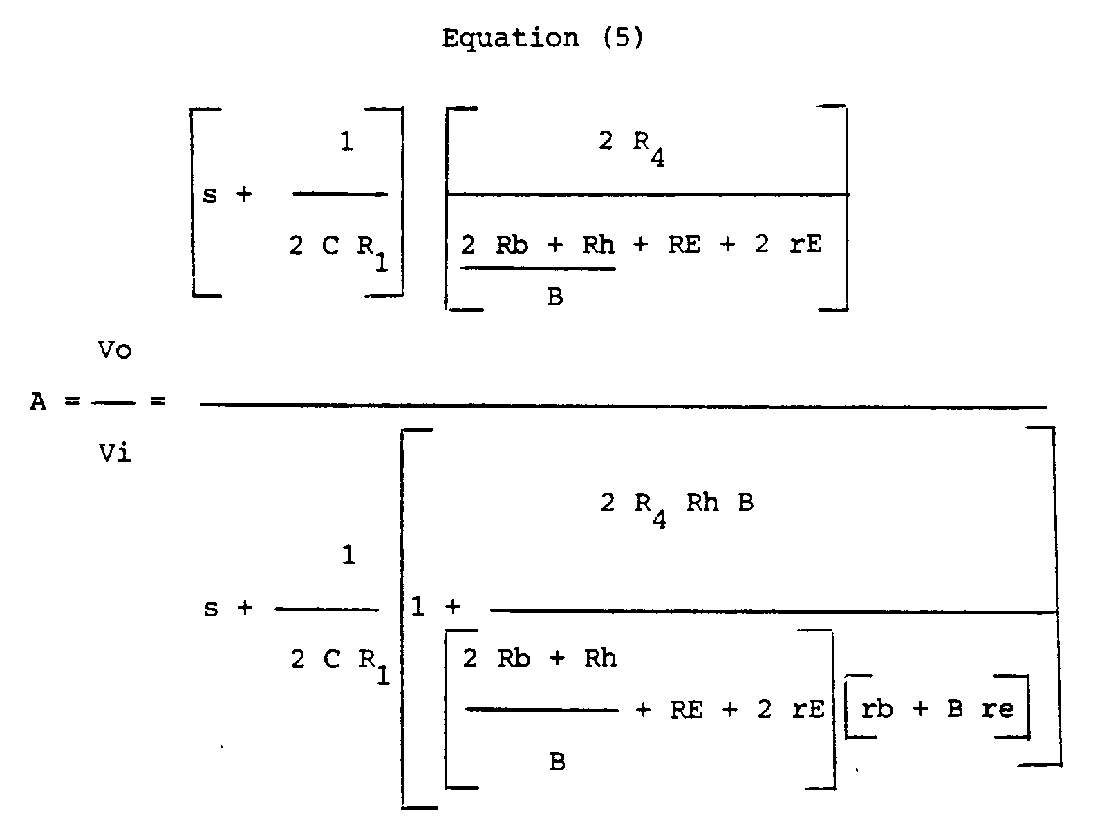
for ft >> fpole where terms for Equation (5) are defined elsewhere in the specification. - Voltage gain transfer function at high frequencies for the circuit of Fig. 6 is given by

- Voltage gain transfer function at low frequencies for the circuit of Fig. 6 is given by

- Transfer functions (5), (6) and (7) are approximate in that they do not consider the transition frequency of transistors nor transistor forward current gain variations. The amplifier of Fig. 6 also has a high pass frequency characteristic.
- As in the circuit configuration of Figs. 4 and 5, feed-forward control is used to minimise DC offset at the output. Current source J0 supplies an offset current through the activated Rh. The optimum value of such offset current may be estimated by the relation

- In a manner similar to that for the circuit configuration of Figs. 4 and 5, the transconductance amplifier gain and the current available to charge or discharge capacitor C can be increased to control switchover transient settling time of the circuit. The increase of gain and charge or discharge current is provided in the same manner as previously described for the circuit configurations of Figs. 4 and 5. Alternatively, switchover transient recovery time can be controlled by using the circuit of Fig. 7B, the operation of which is described in European Patent Application No. EP-A-0 241 770. Nodes 5, 6A and 6B are identified to indicate connection of this circuit at correspondingly identified nodes of the circuit of Fig. 6.

The voltage gain transfer function at low frequencies is given by:

Claims (14)
- A circuit for biasing a magnetoresistive sensor at a constant bias voltage and for amplifying signals produced thereby, said circuit comprising:
a magnetoresistive sensor (Rh) having a steady state resistance value;
amplifier means having an input stage responsive to voltage deviations from said constant bias voltage value across said sensor (Rh) to produce at an output stage of said amplifier means an amplified output signal representing the change in the steady state resistance value of the sensor (Rh) arising from changes in the magnetic field to which the sensor (Rh) is exposed;
said input stage including at least two transistors (T1a, T1b) coupled in differential pair configuration and having the magnetoresistive sensor coupled between the bases of said pair of transistors (T1a, T1b), and an emitter resistor (RE) coupled between the emitters of said differential pair of transistors (T1a, T1b), the emitter of one transistor of said pair of transistors (T1a, T1b) being coupled to a first constant current source (J1), said amplifier means including link means coupling said emitter resistor (RE) to the bases of said differential pair of transistors (T1a, T1b), whereby said bias voltage is referenced to a voltage produced by a current from said first constant current source (J1) flowing through said emitter resistor (RE). - A circuit as claimed in claim 1, wherein the current flowing in each of the emitters of said differential pair of transistors (T1a, T1b) is substantially equal.
- A circuit as claimed in any preceding claim, wherein the output stage comprises two resistors (R4a, R4b) having substantially equal resistance value.
- A circuit as claimed in any preceding claim wherein said link means comprises feedback means coupled from the output stage to the input stage for correcting variations in said bias voltage levels.
- A circuit as claimed in claim 4, wherein the collectors and bases of said first differential pair of transistors (T1a, T1b) are coupled to the feedback means and the emitters of said first differential pair are coupled to the first constant current source.
- A circuit as claimed in claim 4 or claim 5, wherein the feedback means includes:
at least two transistors (T4a, T4b) coupled in a second differential pair configuration for correcting the voltage at the bases of the first differential pair; and
first and second follower transistors (T3a, T3b), coupled to the first differential pair of transistors (T1a, T1b), for coupling the variations in the voltage produced in the input stage to the second differential pair of transistors (T4a, T4b);
said second differential pair being coupled to a second constant current source (J4), and said follower transistors (T3a, T3b) being coupled to third (J3a) and fourth (J3b) constant current sources, respectively. - A circuit as claimed in any preceding claim, further including feedforward means, coupled to the input and output stages, for controlling the DC offset voltage at the output of the output stage.
- A circuit as claimed in any of claims 4 to 7, wherein the feedback means includes frequency setting means to set the frequency response of the circuit.
- A circuit as claimed in claim 8, wherein the frequency setting means is a capacitor.
- A circuit as claimed in any preceding claim, further including:
a plurality of input stages (G,...Gn); and
selection means for activating one of the plurality of input stages and deactivating all of the remaining plurality of input stages. - A circuit as claimed in claim 10, further including settling means for reducing the time required for said circuit to settle into steady-state operation after one of said plurality of input stages is deactivated and another of said input stages is activated or after activating any input stage.
- A circuit as claimed in claim 11, wherein the settling means comprise control means for temporarily increasing the available output drive current of said feedback means during activation of any of said plurality of input stages.
- A circuit as in claim 11, wherein the settling means comprises first and second comparator means coupled to the output of said input stage for controlling the DC offset voltage thereat in response to a change in such DC offset voltage during deactivation of one and activation of another input stage.
- A circuit as claimed in any of claims 11 to 13, wherein said selection means is effective for deactivating all of said input stages.
Applications Claiming Priority (2)
| Application Number | Priority Date | Filing Date | Title |
|---|---|---|---|
| US880419 | 1986-06-30 | ||
| US06/880,419 US4786993A (en) | 1986-06-30 | 1986-06-30 | Voltage amplifier for constant voltage biasing and amplifying signals from a MR sensor |
Publications (3)
| Publication Number | Publication Date |
|---|---|
| EP0251023A2 EP0251023A2 (en) | 1988-01-07 |
| EP0251023A3 EP0251023A3 (en) | 1988-08-24 |
| EP0251023B1 true EP0251023B1 (en) | 1992-09-02 |
Family
ID=25376242
Family Applications (1)
| Application Number | Title | Priority Date | Filing Date |
|---|---|---|---|
| EP87108643A Expired EP0251023B1 (en) | 1986-06-30 | 1987-06-16 | A circuit for biasing a magnetoresistive sensor and amplifying signals produced thereby |
Country Status (5)
| Country | Link |
|---|---|
| US (1) | US4786993A (en) |
| EP (1) | EP0251023B1 (en) |
| JP (1) | JPS639002A (en) |
| CA (1) | CA1326072C (en) |
| DE (1) | DE3781471T2 (en) |
Families Citing this family (40)
| Publication number | Priority date | Publication date | Assignee | Title |
|---|---|---|---|---|
| JPH0216475A (en) * | 1988-07-04 | 1990-01-19 | Sharp Corp | Superconducting magnetism measuring instrument |
| US4879610A (en) * | 1988-09-28 | 1989-11-07 | International Business Machines Corporation | Protective circuit for a magnetoresistive element |
| US5227212A (en) * | 1989-03-16 | 1993-07-13 | International Business Machines Corporation | Magnetic recording disk, magnetoresistive read head, inductive write head combination |
| US5032935A (en) * | 1989-12-12 | 1991-07-16 | International Business Machines Corporation | Amplification of signals produced by a magnetoresistive element |
| US5103353A (en) * | 1990-05-01 | 1992-04-07 | International Business Machines Corporation | Low noise amplifier with short circuit protection for signals from magnetoresistive element |
| US5122915A (en) * | 1990-09-26 | 1992-06-16 | Minnesota Mining And Manufacturing Company | Low-noise preamplifier for magneto-resistive heads |
| US5204789A (en) * | 1991-01-31 | 1993-04-20 | International Business Machines Corporation | Low noise voltage-biasing amplifier for magnetoresistive element |
| JP3109889B2 (en) * | 1992-01-30 | 2000-11-20 | 株式会社日立製作所 | Circuit for magnetic head |
| US5309294A (en) * | 1992-09-08 | 1994-05-03 | Rocky Mountain Magnetics, Inc. | Method and circuitry to provide true voltage bias to a magnetoresistive head |
| US5323278A (en) * | 1992-09-17 | 1994-06-21 | International Business Machines Corporation | Low noise amplifier circuit for magnetoresistive sensors for fast read-write switching in low supply voltage applications |
| US5309295A (en) * | 1992-10-08 | 1994-05-03 | International Business Machines Corporation | Method and apparatus for biasing a magneto-resistive head |
| US5327303A (en) * | 1992-12-18 | 1994-07-05 | Seagate Technology, Inc. | MR preamplifier having feedback loops for minimizing differential low frequency components and regulating common mode low frequency components of the preamplifier output signal |
| US5455730A (en) * | 1993-02-18 | 1995-10-03 | International Business Machines Corporation | Contact magnetic recording disk file with a magnetoresistive read sensor |
| JP2994522B2 (en) * | 1993-02-22 | 1999-12-27 | 富士通株式会社 | Preamplifier for magnetoresistive element |
| US5398144A (en) * | 1993-02-25 | 1995-03-14 | Vtc Inc. | Bias generator for a low voltage differential read amplifier |
| US5442492A (en) * | 1993-06-29 | 1995-08-15 | International Business Machines Corporation | Data recovery procedure using DC offset and gain control for timing loop compensation for partial-response data detection |
| US5712739A (en) * | 1993-11-08 | 1998-01-27 | Kabushiki Kaisha Toshiba | Magnetic disk drive system with a composite head unit including a magnetoresistive read only head and an inductive write only head |
| US5444579A (en) * | 1993-12-17 | 1995-08-22 | Imp, Inc. | Preamplifier of a signal from a variable resistance sensor, and a current source |
| US5426542A (en) * | 1994-01-21 | 1995-06-20 | Seagate Technology, Inc. | Electronically coupled high-impedance magnetoresistive preamplifier |
| US5465186A (en) * | 1994-01-26 | 1995-11-07 | International Business Machines Corporation | Shorted magnetoresistive head leads for electrical overstress and electrostatic discharge protection during manufacture of a magnetic storage system |
| US5877911A (en) * | 1996-03-13 | 1999-03-02 | International Business Machines Corporation | Magneto-resistive head pre-amplifying circuit for avoiding output voltage transients |
| US5774291A (en) * | 1996-03-28 | 1998-06-30 | International Business Machines Corporation | Voltage measurement circuit for a magnetoresistive head installed in a disk enclosure |
| US6038090A (en) | 1996-04-03 | 2000-03-14 | International Business Machines Corporation | Method and apparatus for improving baseline recovery of an MR head using a programmable recovery time constant |
| US5914630A (en) * | 1996-05-10 | 1999-06-22 | Vtc Inc. | MR head preamplifier with output signal amplitude which is independent of head resistance |
| US6061192A (en) * | 1996-08-19 | 2000-05-09 | Texas Instruments Incorporated | Method and circuit for providing feedback in a pre-amplifier for a multi-head disk drive |
| US5986839A (en) * | 1996-09-17 | 1999-11-16 | International Business Machines Corporation | Electronic magnetoresistive sensor biasing using a transducer equivalent circuit and current sources |
| US5790334A (en) * | 1996-10-02 | 1998-08-04 | International Business Machines Corporation | Circuit and method for optimizing bias supply in a magnetoresistive head based on the thermal properties of the MR head itself |
| US5856891A (en) * | 1997-01-22 | 1999-01-05 | Vtc Inc. | MR resistive-biasing scheme providing low noise high common-mode rejection and high supply rejection |
| US6219195B1 (en) | 1998-01-29 | 2001-04-17 | Marvell Technology Group Ltd. | Low-noise magneto-resistive amplifier using CMOS technology |
| US6252735B1 (en) | 1999-02-25 | 2001-06-26 | International Business Machines Corporation | Voltage-biasing, voltage-sensing differential preamplifier for magnetoresistive elements |
| US6606212B1 (en) | 1999-03-17 | 2003-08-12 | International Business Machines Corporation | Wideband readout of magneto-resistive heads for data storage |
| US6215302B1 (en) * | 1999-05-04 | 2001-04-10 | National Semiconductor Corporation | Preamplifier and method for measuring resistance of a resistive transducer |
| EP1333427A3 (en) * | 2002-01-31 | 2008-04-30 | Texas Instruments Incorporated | Circuit for reading differential data from a disk by applying a voltage bias on a read head |
| US6822817B2 (en) * | 2002-10-31 | 2004-11-23 | International Business Machines Corporation | Preamplifier circuit suitable for use in magnetic storage devices |
| EP1641116A1 (en) * | 2004-09-27 | 2006-03-29 | STMicroelectronics S.r.l. | Reduced hardware control circuit device with current loop for broad band hard disk drive applications |
| US8269491B2 (en) * | 2008-02-27 | 2012-09-18 | Allegro Microsystems, Inc. | DC offset removal for a magnetic field sensor |
| EP2784521B1 (en) | 2013-03-28 | 2019-04-17 | Fraunhofer-Gesellschaft zur Förderung der angewandten Forschung e.V. | Sensor apparatus and method |
| EP2878927B1 (en) | 2013-11-29 | 2016-10-26 | Fraunhofer-Gesellschaft zur Förderung der angewandten Forschung e.V. | Sensor circuit for measuring a physical quantity |
| WO2017099991A1 (en) * | 2015-12-08 | 2017-06-15 | Cooper Technologies Company | Constant power supply for thermo-electric cells |
| IT202300001830A1 (en) * | 2023-02-06 | 2024-08-06 | St Microelectronics Int Nv | HARD DISK DRIVE OPERATION PROCEDURE, CONTROL CIRCUIT, CORRESPONDING HARD DISK DRIVE AND COMPUTER DEVICE |
Family Cites Families (13)
| Publication number | Priority date | Publication date | Assignee | Title |
|---|---|---|---|---|
| US3551706A (en) * | 1968-10-15 | 1970-12-29 | Bell Inc F W | Hall effect device configurations for extended frequency range |
| JPS493585U (en) * | 1972-04-10 | 1974-01-12 | ||
| US3816766A (en) * | 1973-01-29 | 1974-06-11 | Sprague Electric Co | Integrated circuit with hall cell |
| US3979775A (en) * | 1975-09-08 | 1976-09-07 | International Business Machines Corporation | Magnetoresistive multitransducer assembly with compensation elements for thermal drift and bias balancing |
| US4050086A (en) * | 1976-05-06 | 1977-09-20 | International Business Machines Corporation | Dynamic transducer biasing signal amplifying circuitry |
| US4159537A (en) * | 1978-05-01 | 1979-06-26 | Burroughs Corporation | Bubble detector-dynamic level signal shifting |
| US4191977A (en) * | 1978-09-29 | 1980-03-04 | International Business Machines Corporation | Biasing of magnetoresistive read head using gyrators |
| US4242693A (en) * | 1978-12-26 | 1980-12-30 | Fairchild Camera & Instrument Corporation | Compensation of VBE non-linearities over temperature by using high base sheet resistivity devices |
| JPS58189804A (en) * | 1982-04-30 | 1983-11-05 | Fujitsu Ltd | Bias system of head using magneto-resistance effect element |
| CH659917A5 (en) * | 1982-06-16 | 1987-02-27 | Landis & Gyr Ag | MAGNETIC SENSOR. |
| NL8300557A (en) * | 1983-02-15 | 1984-09-03 | Philips Nv | MAGNETIC FIELD SENSOR. |
| CA1248222A (en) * | 1984-08-27 | 1989-01-03 | Yutaka Souda | Magnetic transducer head utilizing magnetoresistance effect |
| US4706138A (en) * | 1986-04-14 | 1987-11-10 | International Business Machines Corporation | Amplification of signals produced by a magnetic sensor |
-
1986
- 1986-06-30 US US06/880,419 patent/US4786993A/en not_active Expired - Lifetime
-
1987
- 1987-04-15 CA CA000534767A patent/CA1326072C/en not_active Expired - Fee Related
- 1987-04-20 JP JP62095517A patent/JPS639002A/en active Pending
- 1987-06-16 DE DE8787108643T patent/DE3781471T2/en not_active Expired - Fee Related
- 1987-06-16 EP EP87108643A patent/EP0251023B1/en not_active Expired
Also Published As
| Publication number | Publication date |
|---|---|
| EP0251023A2 (en) | 1988-01-07 |
| DE3781471T2 (en) | 1993-04-08 |
| DE3781471D1 (en) | 1992-10-08 |
| JPS639002A (en) | 1988-01-14 |
| EP0251023A3 (en) | 1988-08-24 |
| US4786993A (en) | 1988-11-22 |
| CA1326072C (en) | 1994-01-11 |
Similar Documents
| Publication | Publication Date | Title |
|---|---|---|
| EP0251023A2 (en) | A circuit for biasing a magnetoresistive sensor and amplifying signals produced thereby | |
| EP0455472B1 (en) | Low noise amplifier with short circuit protection for signals from magnetoresistive element | |
| US4706138A (en) | Amplification of signals produced by a magnetic sensor | |
| EP0361781B1 (en) | Protective circuit for magnetoresistive element | |
| US5309295A (en) | Method and apparatus for biasing a magneto-resistive head | |
| US6134060A (en) | Current bias, current sense for magneto-resistive preamplifier, preamplifying integrated circuit, and related methods | |
| US6429700B1 (en) | Driver circuit with output common mode voltage control | |
| US6341046B1 (en) | Current biasing voltage sensing preamplifier for magnetoresistive heads | |
| EP0439299A2 (en) | A circuit for suppressing additive disturbances in data channels | |
| JPH06169227A (en) | Amplifier circuit | |
| US5914630A (en) | MR head preamplifier with output signal amplitude which is independent of head resistance | |
| US4460873A (en) | Active differential output direct current offset voltage compensation circuit for a differential amplifier | |
| US7251091B2 (en) | Current-sense bias circuit for a magnetoresistive head and method of sensing a current therethrough | |
| US6710959B1 (en) | Input pole compensation for a disk drive read head | |
| US5717536A (en) | Single-ended cascode amplifier for magnetoresistive sensors | |
| EP0265763A2 (en) | Frequency response compensation circuit | |
| US7724460B2 (en) | Magneto-resistive head resistance sensor | |
| US6275347B1 (en) | Current bias, current sense preamplifier for a magnetoresistive reader | |
| US6211736B1 (en) | Signal amplifying circuit for magnetoresistive element | |
| US6473253B1 (en) | Read channel with programmable bandwidth control | |
| US6175276B1 (en) | Indirect emitter-coupling preamplifier for magneto-resistive heads with single-ended feedback | |
| JPH1166505A (en) | Low noise preamplifier for magnetoresistive data converter. | |
| US6920002B2 (en) | Reproducing amplifier and magnetic recording and reproducing apparatus employing the reproducing amplifier | |
| US6549357B1 (en) | Selectable input pole compensation for a disk drive read head | |
| US6208482B1 (en) | Signal amplifying circuit for an MR element |
Legal Events
| Date | Code | Title | Description |
|---|---|---|---|
| PUAI | Public reference made under article 153(3) epc to a published international application that has entered the european phase |
Free format text: ORIGINAL CODE: 0009012 |
|
| AK | Designated contracting states |
Kind code of ref document: A2 Designated state(s): DE FR GB IT |
|
| 17P | Request for examination filed |
Effective date: 19880426 |
|
| PUAL | Search report despatched |
Free format text: ORIGINAL CODE: 0009013 |
|
| AK | Designated contracting states |
Kind code of ref document: A3 Designated state(s): DE FR GB IT |
|
| 17Q | First examination report despatched |
Effective date: 19910403 |
|
| GRAA | (expected) grant |
Free format text: ORIGINAL CODE: 0009210 |
|
| AK | Designated contracting states |
Kind code of ref document: B1 Designated state(s): DE FR GB IT |
|
| PG25 | Lapsed in a contracting state [announced via postgrant information from national office to epo] |
Ref country code: IT Free format text: LAPSE BECAUSE OF FAILURE TO SUBMIT A TRANSLATION OF THE DESCRIPTION OR TO PAY THE FEE WITHIN THE PRE;WARNING: LAPSES OF ITALIAN PATENTS WITH EFFECTIVE DATE BEFORE 2007 MAY HAVE OCCURRED AT ANY TIME BEFORE 2007. THE CORRECT EFFECTIVE DATE MAY BE DIFFERENT FROM THE ONE RECORDED.SCRIBED TIME-LIMIT Effective date: 19920902 |
|
| REF | Corresponds to: |
Ref document number: 3781471 Country of ref document: DE Date of ref document: 19921008 |
|
| ET | Fr: translation filed | ||
| PGFP | Annual fee paid to national office [announced via postgrant information from national office to epo] |
Ref country code: GB Payment date: 19930525 Year of fee payment: 7 |
|
| PGFP | Annual fee paid to national office [announced via postgrant information from national office to epo] |
Ref country code: FR Payment date: 19930601 Year of fee payment: 7 |
|
| PLBE | No opposition filed within time limit |
Free format text: ORIGINAL CODE: 0009261 |
|
| STAA | Information on the status of an ep patent application or granted ep patent |
Free format text: STATUS: NO OPPOSITION FILED WITHIN TIME LIMIT |
|
| PGFP | Annual fee paid to national office [announced via postgrant information from national office to epo] |
Ref country code: DE Payment date: 19930712 Year of fee payment: 7 |
|
| 26N | No opposition filed | ||
| PG25 | Lapsed in a contracting state [announced via postgrant information from national office to epo] |
Ref country code: GB Effective date: 19940616 |
|
| GBPC | Gb: european patent ceased through non-payment of renewal fee |
Effective date: 19940616 |
|
| PG25 | Lapsed in a contracting state [announced via postgrant information from national office to epo] |
Ref country code: FR Effective date: 19950228 |
|
| PG25 | Lapsed in a contracting state [announced via postgrant information from national office to epo] |
Ref country code: DE Effective date: 19950301 |
|
| REG | Reference to a national code |
Ref country code: FR Ref legal event code: ST |