EP0243499B1 - Electronic device having a power supply input circuit in which noise from static electricity is suppressed - Google Patents
Electronic device having a power supply input circuit in which noise from static electricity is suppressed Download PDFInfo
- Publication number
- EP0243499B1 EP0243499B1 EP86900257A EP86900257A EP0243499B1 EP 0243499 B1 EP0243499 B1 EP 0243499B1 EP 86900257 A EP86900257 A EP 86900257A EP 86900257 A EP86900257 A EP 86900257A EP 0243499 B1 EP0243499 B1 EP 0243499B1
- Authority
- EP
- European Patent Office
- Prior art keywords
- static electricity
- circuit
- input
- input line
- line
- Prior art date
- Legal status (The legal status is an assumption and is not a legal conclusion. Google has not performed a legal analysis and makes no representation as to the accuracy of the status listed.)
- Expired - Lifetime
Links
Images


Classifications
-
- B—PERFORMING OPERATIONS; TRANSPORTING
- B01—PHYSICAL OR CHEMICAL PROCESSES OR APPARATUS IN GENERAL
- B01J—CHEMICAL OR PHYSICAL PROCESSES, e.g. CATALYSIS OR COLLOID CHEMISTRY; THEIR RELEVANT APPARATUS
- B01J21/00—Catalysts comprising the elements, oxides, or hydroxides of magnesium, boron, aluminium, carbon, silicon, titanium, zirconium, or hafnium
- B01J21/16—Clays or other mineral silicates
-
- B—PERFORMING OPERATIONS; TRANSPORTING
- B01—PHYSICAL OR CHEMICAL PROCESSES OR APPARATUS IN GENERAL
- B01J—CHEMICAL OR PHYSICAL PROCESSES, e.g. CATALYSIS OR COLLOID CHEMISTRY; THEIR RELEVANT APPARATUS
- B01J29/00—Catalysts comprising molecular sieves
- B01J29/04—Catalysts comprising molecular sieves having base-exchange properties, e.g. crystalline zeolites
- B01J29/049—Pillared clays
-
- C—CHEMISTRY; METALLURGY
- C07—ORGANIC CHEMISTRY
- C07C—ACYCLIC OR CARBOCYCLIC COMPOUNDS
- C07C1/00—Preparation of hydrocarbons from one or more compounds, none of them being a hydrocarbon
- C07C1/02—Preparation of hydrocarbons from one or more compounds, none of them being a hydrocarbon from oxides of a carbon
- C07C1/04—Preparation of hydrocarbons from one or more compounds, none of them being a hydrocarbon from oxides of a carbon from carbon monoxide with hydrogen
- C07C1/0425—Catalysts; their physical properties
- C07C1/043—Catalysts; their physical properties characterised by the composition
-
- C—CHEMISTRY; METALLURGY
- C07—ORGANIC CHEMISTRY
- C07C—ACYCLIC OR CARBOCYCLIC COMPOUNDS
- C07C2/00—Preparation of hydrocarbons from hydrocarbons containing a smaller number of carbon atoms
- C07C2/54—Preparation of hydrocarbons from hydrocarbons containing a smaller number of carbon atoms by addition of unsaturated hydrocarbons to saturated hydrocarbons or to hydrocarbons containing a six-membered aromatic ring with no unsaturation outside the aromatic ring
- C07C2/64—Addition to a carbon atom of a six-membered aromatic ring
- C07C2/66—Catalytic processes
-
- H—ELECTRICITY
- H03—ELECTRONIC CIRCUITRY
- H03K—PULSE TECHNIQUE
- H03K17/00—Electronic switching or gating, i.e. not by contact-making and –breaking
- H03K17/16—Modifications for eliminating interference voltages or currents
-
- H—ELECTRICITY
- H03—ELECTRONIC CIRCUITRY
- H03K—PULSE TECHNIQUE
- H03K19/00—Logic circuits, i.e. having at least two inputs acting on one output; Inverting circuits
- H03K19/003—Modifications for increasing the reliability for protection
- H03K19/00346—Modifications for eliminating interference or parasitic voltages or currents
-
- C—CHEMISTRY; METALLURGY
- C07—ORGANIC CHEMISTRY
- C07C—ACYCLIC OR CARBOCYCLIC COMPOUNDS
- C07C2529/00—Catalysts comprising molecular sieves
- C07C2529/04—Catalysts comprising molecular sieves having base-exchange properties, e.g. crystalline zeolites, pillared clays
- C07C2529/05—Pillared clays
Definitions
- the present invention relates to an electronic device having a power supply input circuit in which noise from static electricity is suppressed.
- the invention is particularly applicable to small portable electronic devices and small data devices for preventing them from being erroneously operated or from being broken down by the static electricity.
- Portable electronic devices such as IC cards, cameras, wristwatches, and those electronic devices that are not grounded, are prone to be erroneously operated or broken down due to the phenomena of static electricity.
- Such devices have heretofore been prevented from erroneously operating or from breaking down in the same manner as those electronic devices that can be usually grounded.
- a reference potential of a grounding circuit Using a reference potential of a grounding circuit, however, the noise can be suppressed efficiently over a frequency region which is lower than that of the VHF band. Even if one or more points are grounded, the grounding circuit is not quite effective in absorbing the electromagnetic waves of large energy that are generated when the static electricity is discharged. Therefore, the noise must be suppressed from quite a novel point of view.
- OTT. Bell Laboratory, U.S.A., translated by Takao Matsui.
- a pattern of circuit board of a potential of the active side that is formed to absorb noise, works as an antenna
- the structure connected to the potential of the active side of the metal housing to accomplish the grounding works as an antenna. That is, with the pattern of circuit board that is not grounded or with the structure connected to the potential of the active side of the metal housing to accomplish the grounding, the electromagnetic waves are absorbed and are converted into eddy current to produce noise in the circuit network.
- FIG. 7 is a circuit diagram schematically illustrating an input circuit.
- a capacity Ca exists between the active side 2 and the input line 4
- a capacity Cp exists between the pull side 3 and the input line 4.
- a relationship Ca>Cp is described. It is obvious that electromagnetic waves generated by the static electricity or the like are simultaneously superimposed as an impulse on the active side 2 and on the pull side 3 of the power source voltage. Therefore, the potential appearing on the input line 4 forms a potential on the active side 2 via Ca.
- V8 is a diagram of voltage waveforms that change with the lapse of time, and illustrates erroneous operations of the input circuit of Fig. 7 caused by the static electricity and the like, and wherein V1 denotes an active potential, V2 denotes a pull potential, V3 denotes a potential of the input line which is usually equal to V2, V T denotes a threshold potential of the circuit 1 under the ordinary condition which is equal to V2/2, t denotes a time, t0 denotes a time at a moment when V0 which is the power source voltage is rapidly changed by the static electricity into V2(t0), V2(t0) denotes a potential at the time t0, V3(t0) denotes a potential of the input line that is obtained by dividing V2(t0) by the capacities Ca and Cp, i.e., V2(t0) ⁇ Cp/(Ca + Cp) , V T (t0) denotes a threshold potential of the circuit 1,
- the potential V2(t0) becomes more than 6 thimes as great as the potential under the ordinary condition of the potential V2.
- Fig. 9 is a schematic diagram related to energy of the electromagnetic waves and noise, wherein reference numeral 100 denotes a region which includes all of the electromagnetic waves such as electromagnetic waves (VHF), infrared rays, visible rays, ultraviolet rays, and X-rays.
- the electric discharge is a phenomenon of an avalanche of electrons in which the electrons having a kinetic energy proportional to the voltage impinge upon an opposing metal electrode. Most of the electric charge migrates. The electric charge flows through paths having small impedances.
- the kinetic energy E is converted into electromagnetic waves.
- ⁇ min [ ⁇ ] 12.4/Vmax [Kv]
- the wavelength ⁇ min can be easily calculated. For example, if the charged voltage Vmax is 24.8 Kv, there are generated electromagnetic waves over a wide range, the mininum wavelength thereof being 0.5 angstrom. However, the energy is not all converted.
- the conversion efficiency ⁇ is given by, where,
- Eg an energy gap
- the range is indicated by a region 102 in Fig. 9.
- the noise In the electronic devices, the noise must be suppressed for all of the electromagnetic wave bands (region 104 in Fig. 9).
- the noise In a grounded circuit, the noise can be suppressed by the single-point grounding for the electromagnetic waves of up to the VHF band that is referred to in a radio communications system, and can be suppressed by the many-point grounding for the electromagnetic waves of the UHF band (region where waveguides are handled), which, however, are not omnipotent. That is, interference to the electronic devices caused by the static electricity must be eliminated by a method which does not rely upon the grounding circuit.
- the region based upon a new concept is indicated by 105 in Fig. 9.
- electrically equivalent constants of a human body consist of a resistance of about one kiloohms and an electrostatic capacity of 200 pF to 500 pF.
- Fig. 10 shows electrostatic discharge characteristics for the amount of electric charge (Q) when the charged volatage (V) is 20 Kv, resistance (R) is 800 ohms, and electrostatic capacity (C) is 500 pF.
- the amount of electric charge (Q) is given by, If the side in which the discharge takes place has zero resistance, a discharge time ⁇ given by, is required until the electric charge of 10 ⁇ C is discharged to 1/e. In practice, however, the side in which the discharge takes place has resistance to some extent, and a longer period of time is required for the discharge.
- the oxide film is completely destroyed (scattered). If the device is under the electrically charged condition in which the electric discharge does not take place, the potential of the active side 2 is spread throughout the electronic circuit network that is constituted relying upon the idea of forming a grounding circuit. Therefore, erroneous input and erroneous operation caused by the electric charge take place on the pull side 3, in the input line 4 and in the field-effect IC.
- a semiconductor integrated circuit (IC) chip has many input/output terminals (hereinafter referred to as IC pads).
- IC pads The layout of IC pads will be discussed below. Here, to simplify the description, the layout contains a minimum number of pads.
- Fig. 11 is a model diagram of the layout of IC pads that are mounted on a circuit board and are susceptible to the static electricity.
- Fig. 13 is also a model diagram of the layout of IC pads that are mounted on a circuit board and are susceptible to the static electricity.
- Fig. 12 is a matrix diagram for comparing the positional relations related to the IC pad layout of Fig. 11, and
- Fig. 14 is a matrix diagram for comparing the positional relations related to the IC pad layout of Fig. 13.
- Names of coordinates of matrix are names of functions of IC pads.
- X IN and X OUT denote IC pads that constitute an oscillation circuit
- ⁇ 1 and ⁇ 2 denote IC pads that constitute a booster circuit.
- V DD denotes an IC pad which receives a potential of the active side 2
- V SS denotes an IC pad which receives a potential of the pull side 3.
- SW denotes an IC pad of the circuit 1 which is connected to an end of a switch in the input line 4.
- FIG. 12 which shows the pads that are mounted on the circuit board and are susceptible to the static electricity with the lower left portion of the diagonal line of the matrix diagram of Fig. 14.
- symbols ⁇ that are located at symmetrical positions relative to the diagonal line are replaced by symbols ⁇ .
- the matrix of symbols ⁇ indicates that the layouts of IC pads of Figs. 11 and 13 are in a neighborhood relationship to each other. That is, X IN and X OUT , ⁇ 1 and ⁇ 2, and V DD and SW indicate similar layouts having neighborhood relationship in Figs. 11 and 13.
- a diagram of Fig. 20 for comparing matrixes is described by combining the upper right portion of the diagonal line of the matrix diagram of Fig. 17 corresponding to Fig.
- FIG. 16 which shows the layout of IC pads that are mounted on the circuit board and are confirmed to be little affected by the static electricity, with the lower left portion of the diagonal line of a matrix diagram of Fig. 19 corresponding to Fig. 18 which shows the layout of IC pads that are confirmed to be little affected by the static electricity after they have been mounted.
- symbols ⁇ that are located at symmetrical positions relative to the diagonal line are replaced by symboles ⁇ .
- the matrix of symbols ⁇ indicates that the layouts of IC pads of Figs. 16 and 18 are in a neighborhood relationship to each other. That is, X IN and X OUT , ⁇ 1 and ⁇ 2, and V SS and SW indicate similar layouts having a neighborhood relationship in Figs. 15 and 17.
- the IC that is easily affected by the static electricity after it has been mounted on the circuit board is compared below with the IC that is little affected, in regard to their similar points. If similar points common to the easily affected IC and the little affected IC are eliminated, since they are irrelevant to whether they are little affected or easily affected, the following fact becomes obvious. The results are discussed below. After mounted on the circuit board, the IC tends to be easily affected or little affected by the static electricity because of the reason that V DD (active side 2) has more patterns that stretch on the circuit board than V SS (pull side 3), since the circuit is designed based upon the idea of employing a grounding circuit. This fact is quite important to derive the following hypotheses.
- the IC which is easily affected has V DD and SW (active side 2 and input line 4) that are adjacent to each other. That is, there exists a large stray capacity Ca between the active side 2 and the input line 4.
- the IC which is little affected has V SS and SW (pull side 3 and input line 4) that are adjacent to each other. That is, a stray capacity Cp between the pull side 3 and the input line 4 is smaller than the above-mentioned stray capacity Ca.
- Fig. 21 is a solid diagram of the circuit of a digital wristwatch, in which reference numeral 4a denotes a switch pattern which forms an end of the input line 4, and 2b denotes a switch spring which assumes the potential of the active side 2.
- the switch pattern 4a On the switch pattern 4a is disposed the switch spring 2b in an opposed manner over an area 9 of 10mm2 maintaining a distance of 0.3 mm, to thereby form an air capacitor.
- the device is easily affected by the static electricity and operates erroneously for various control operations. If the shape of the switch spring 2b is so changed that it is opposed to the switch pattern over an area 10 instead of the area 9, then the device becomes little affected by the static electricity. This fact verifies the aforementioned hypothesis 1.
- a capacitor was inserted between the switch pattern 4a and the potential V SS of the pull side 3 under the condition of the opposed area 9, in order to examine the immunity of the device against the static electricity. It was found that the device exhibited immunity if the capacitor had a capacity greater than a given value.
- Fig. 22 is a solid diagram showing another circuit of the electronic wristwatch. The device is little affected by the static electricity when a temporarily formed V DD pattern 11 is not provided on the V DD pattern 2b adjacent to the switch pattern 4a, the V DD pattern 2b assuming the potential of the active side 2.
- the device becomes susceptible to the static electricity and operates erroneously such as displaying incorrect indication.
- This is one of the verifications related to the aforementioned hypothesis 2.
- the idea to lengthen the pattern of the active side 2 on the circuit board or to increase the area conforms to the way of thinking which is based upon the grounding circuit, but is not quite effective to suppress the noise that stems from the static electricity and rather makes the situation worse.
- the present invention seeks to remove the above-mentioned defects and to provide an electronic device that has immunity against the phenomena of static electricity.
- an electronic device having a power supply input circuit arranged for suppressing noise from static electricity, the input circuit comprising a first supply line arranged to be at a first source potential, a second supply line arranged to be at a second source potential, and an input line connected by way of a switch to the first supply line and by way of a resistance to the second supply line, said supply lines supplying power to a circuit of the device, characterised in that the first and second supply lines and the input line have a pattern layout of pads of an IC or leads on a circuit board for the input circuit such that a capacitance C a between the first supply line and the input line and a capacitance C p between the input line and the second supply line maintain a relation C a ⁇ C p .
- a metal housing of the device contains an input circuit which maintains an ordinary potential on the input line by inducing a pull potential on the input line in order to eliminate the induction of an active potential other than that for operating the device, thereby to prevent any erroneous input.
- neither the active side (ground side) of the electronic circuit nor the electronic circuit network is permitted to be electrically connected to the housing in order to interrupt the flow of elecric charge and eddy currents produced by electro-magnetic waves of large energy.
- the housing is made of an insulating material, this helps prevent the distribution of electric field from being disturbed in the electronic circuit, and makes it possible to achieve the desired object.
- Figure 1 is a diagram of an input circuit according to an embodiment of the present invention, wherein Figure 1(a) is a diagram in which the active side 2 assumes the higher potential of the power source voltage, and Figure 1(b) is a diagram in which the active side 2 assumes the lower potential of the power source voltage.
- Reference numeral 1 denotes a circuit
- 3 denotes a pull side
- 4 denotes an input line.
- An end of the input line is connected to a switch SW and the other end thereof is connected to the circuit. If the switch SW is turned on, the input line assumes the potential of the active side 2 and if the switch SW is turned off, the input line assumes the potential of the pull side 3 via a pull resistance Rp.
- An electrostatic capacity between the active side 2 and the input line 4 is denoted by Ca and an electrostatic capacity between the input line 4 and the pull side 3 is denoted by Cp, the electrostatic capacities having a relationship Ca ⁇ Cp.
- Fig. 2 is a diagram of a model layout of IC pads illustrating important portions only according to a particular embodiment of the present invention, wherein Fig. 2(a) is a diagram of a layout of IC pads in a circuit structure in which the active side assumes the higher potential of the power source voltage, and Fig. 2(b) is a diagram of a layout of IC pads in a circuit structure in which the active side 2 assumes the lower potential of the power source voltage.
- a terminal for example, X IN in Figure
- the pad of V DD other than the pad of SW and other than the input pad for testing, is provided between the pad of V DD (active side 2) and the pad of SW (input line 4).
- the device is so designed that the stray capacity is relatively decreased between the active side 2 and the input line 4.
- the capacity Ca is inevitably decreased in the pattern layout on the circuit board.
- a pad for example, ⁇ 2 in Figure
- the pad V SS or SW other than the input pad for testing is provided between the pad V SS (active side 2) and the pad SW (input line 4). That is, the device is so designed that the stray capacity is relatively decreased between the active side 2 and the input line 4. Namely, the capacity Ca is inevitably decreased in the pattern layout on the circuit board.
- Fig. 3 is a diagram of a model layout of IC pads showing important portions only according to a further embodiment of the present invention, wherein Fig. 3(a) is a diagram of a layout of IC pads in a circuit structure in which the active side 2 assumes the higher potential of the power source voltage, and Fig. 3(b) is a diagram of a layout of IC pads in a circuit structure in which the active side 2 assumes the lower potential of the power source voltage.
- the pad SW input line 4
- the pad V SS pulse side 3
- Fig. 4 is a diagram showing a portion of the layout of circuit board patterns according to a still further embodiment of the present invention, wherein reference numeral 2c denotes active pattern lines, 5 denotes a pattern other than the active pattern lines, other than the SW pattern lines and other than the pattern lines for testing. Symbols SW1, SW2 and SW3 denote switch patterns, and reference numeral 6 denotes an IC chip.
- the pattern 5 is formed between the active pattern lines 2ca and the pattern SW3, so that the electrostatic capacity Ca is relatively decreased between the active side 2 and the switch pattern SW3 so as to realize the relationship Ca ⁇ Cp mentioned in Fig. 1.
- Fig. 5 is a diagram showing a portion of the layout of circuit board patterns according to a yet further embodiment of the present invention, wherein reference numeral 3a denotes pull pattern lines formed adjacent to SW1 and SW3 pattern lines.
- the electrostatic capacity Cp is relatively increased between the pull side 2 and the SW to achieve the relationship Ca ⁇ Cp mentioned with reference to Fig. 1.
- the layout is so designed that the relationship Ca ⁇ Cp is maintained in any portion of the pattern lines inclusive of, for example, through-holes.
- Fig. 6 is a diagram showing the structure of an electronic device in which the electronic circuit network 8 of the present invention illustrated in Figs. 1, 2, 3, 4 and 5 is contained in the metal housing 7 according to another embodiment of the present invention.
- the metal housing 7 is not electrically conducted to the electronic circuit network 8, so that the electric charge will not flow into the electronic circuit network 8.
- the kinetic energy of electrons that have impinged upon the metal housing 7 is converted into electromagnetic waves of large energy, and whereby the metal housing 7 works as an antenna to absorb the electromagnetic waves that turn into eddy currents.
- the eddy currents are transformed into heat in the metal housing 7 and do not flow into the electronic circuit network 8.
- the electronic device is not adversely affected by the phenomena of static electricity owing to the relationship Ca ⁇ Cp which is the basis of the present invention.
- the embodiments of the present invention completely preclude advsese effects (a), (b), (c) and (d) caused by the static electricity from acting upon the electronic devices.
- the present invention can be effectively adapted to electronic devices for medical uses and electronic devices to be mounted on aircraft that must not be affected by the phenomena of static electricity, lightning or the external electric field, as well as to electronic devices to be mounted on artificial satellites, for meteorological observations and for atomic utilization that are subject to be exposed to ionizing radiation, corpuscular radiation and charged particles.
- the invention can be very effectively adapted to robots, IC cards, electronic computers, electronic measuring instruments, electronic cameras, electronic wristwatches and the like.
Landscapes
- Chemical & Material Sciences (AREA)
- Organic Chemistry (AREA)
- Chemical Kinetics & Catalysis (AREA)
- Engineering & Computer Science (AREA)
- Materials Engineering (AREA)
- Dispersion Chemistry (AREA)
- General Engineering & Computer Science (AREA)
- Mathematical Physics (AREA)
- Physics & Mathematics (AREA)
- General Chemical & Material Sciences (AREA)
- Oil, Petroleum & Natural Gas (AREA)
- Computing Systems (AREA)
- Crystallography & Structural Chemistry (AREA)
- Computer Hardware Design (AREA)
- Elimination Of Static Electricity (AREA)
- Semiconductor Integrated Circuits (AREA)
- Electronic Switches (AREA)
Abstract
Description
- The present invention relates to an electronic device having a power supply input circuit in which noise from static electricity is suppressed. The invention is particularly applicable to small portable electronic devices and small data devices for preventing them from being erroneously operated or from being broken down by the static electricity.
- Portable electronic devices such as IC cards, cameras, wristwatches, and those electronic devices that are not grounded, are prone to be erroneously operated or broken down due to the phenomena of static electricity.
- Such devices have heretofore been prevented from erroneously operating or from breaking down in the same manner as those electronic devices that can be usually grounded. Using a reference potential of a grounding circuit, however, the noise can be suppressed efficiently over a frequency region which is lower than that of the VHF band. Even if one or more points are grounded, the grounding circuit is not quite effective in absorbing the electromagnetic waves of large energy that are generated when the static electricity is discharged. Therefore, the noise must be suppressed from quite a novel point of view.
- Many examples to cope with this problem have been introduced in, for example, Electronics System, "Materials To Cope With Troubles Caused by Static Electricity" compiled by Norio Murasaki, entitled "Section 6, Countermeasures 5.6.2.3. Against Static Electricity in ECR, Electronic Circuit and Printed Board, pp. 222-224. However, many technicians are empirically aware of the fact that there is no simple method which offers sufficiently desirable effects. Concretely speaking, it has been attempted to absorb noise by extending the pattern of the ground side of the circuit board having the potential of the active side or to increase the width of the pattern, or by a method taught in "Grounding of Housing", p, 84, "Practical Method of Decreasing Noise", Henry W. OTT., Bell Laboratory, U.S.A., translated by Takao Matsui. With the portable electronic devices which are not allowed to be grounded, however, noise is not emitted to the ground, and the concept of grounding cannot be pursued. In the electronic devices that cannot be grounded, a pattern of circuit board of a potential of the active side, that is formed to absorb noise, works as an antenna, and the structure connected to the potential of the active side of the metal housing to accomplish the grounding, works as an antenna. That is, with the pattern of circuit board that is not grounded or with the structure connected to the potential of the active side of the metal housing to accomplish the grounding, the electromagnetic waves are absorbed and are converted into eddy current to produce noise in the circuit network. Furthermore, under the condition where the electric charge is not discharged, the lines assuming the potential of the active side of floated ground work to increase the difference of electric field distribution relative to the pull side. This becomes a cause of erroneous operation for the field effect IC's.
- Under such circumstances, three lines, i.e. an
active side 2, aninput line 4, and apull side 3 as shown in an input circuit illustrated in Figure 7, establish an electrically important relationship. The problems that are not solved by the prior art are described below with reference to Figure 7, which is a circuit diagram schematically illustrating an input circuit. In this circuit, a capacity Ca exists between theactive side 2 and theinput line 4, and a capacity Cp exists between thepull side 3 and theinput line 4. A relationship Ca>Cp is described. It is obvious that electromagnetic waves generated by the static electricity or the like are simultaneously superimposed as an impulse on theactive side 2 and on thepull side 3 of the power source voltage. Therefore, the potential appearing on theinput line 4 forms a potential on theactive side 2 via Ca. With a relationship Ca > Cp being maintained, a potential on thepull side 3 also appears on Cp but a potential on theactive side 2 appears on Ca. As a result, the potential on theinput line 4 appears on Ca of an amount that corresponds to the difference between the potential on thepull side 3 and that on theactive side 2. Accordingly, even if the switch SW is not closed, the potential of theinput line 4 has some time to produce the potential on theactive side 2. Under this condition, the input circuit operates erroneously even when the switch SW is not operated. A resistance Rp constitutes pull means, and acircuit 1 is provided in a stage which succeeds the switch SW. Fig. 8 is a diagram of voltage waveforms that change with the lapse of time, and illustrates erroneous operations of the input circuit of Fig. 7 caused by the static electricity and the like, and wherein V₁ denotes an active potential, V₂ denotes a pull potential, V₃ denotes a potential of the input line which is usually equal to V₂, VT denotes a threshold potential of thecircuit 1 under the ordinary condition which is equal to V₂/2, t denotes a time, t₀ denotes a time at a moment when V₀ which is the power source voltage is rapidly changed by the static electricity into V₂(t₀), V₂(t₀) denotes a potential at the time t₀, V₃(t₀) denotes a potential of the input line that is obtained by dividing V₂(t₀) by the capacities Ca and Cp, i.e.,
circuit 1, i.e., V₂(t₀)/2, V₂(t) denotes a power source voltage which is given by a function of the time t, and its time constant is nearly equal to C·r where C denotes a resultant capacity consisting of capacities Ca, Cp, and a capacity of noise source, and r denotes an internal resistance of the power source, V₃(t) denotes a potential of theinput line 4 given by a function of the time t, i.e., given by
circuit 1 given by the function of the time t. - The device will be concretely described in conjunction with Figs. 7 and 8. A man who is electrically charged may produce a voltage in excess of 10 Kv presenting a serious problem in handling electronic devices or portable electronic devices that are not permitted to be grounded. Here, if the potential V₂ rapidly increases to V₂(t₀) at the time t₀ due to noise of electromagnetic waves produced by the electric discharge, the threshold potential

circuit 1 changes into

input line 4 changes into
input line 4 is apt to reach the threshold voltage

For instance, if the capacities have a relation

input line 4 reaches the threshold voltage
- The above way of thinking is supported by means for deriving a hypothesis that will be described below, and by the experiment and investigation using practical electronic devices. Described below are the concept related to improve the immunity against the static electricity, means for deriving the hypothesis, and experiment to prove the hypothesis.
- Fig. 9 is a schematic diagram related to energy of the electromagnetic waves and noise, wherein
reference numeral 100 denotes a region which includes all of the electromagnetic waves such as electromagnetic waves (VHF), infrared rays, visible rays, ultraviolet rays, and X-rays. The electric discharge is a phenomenon of an avalanche of electrons in which the electrons having a kinetic energy proportional to the voltage impinge upon an opposing metal electrode. Most of the electric charge migrates. The electric charge flows through paths having small impedances. Here, what is important is to construct the device that the electric charge does not pass through the electronic circuit network. Upon impingement, the kinetic energy E is converted into electromagnetic waves. The kinetic energy E of an electron is given by,

The energy is conserved and is converted into electromagnetic waves, i.e.,

The wavelength λ becomes a minimum at a point where the charged voltage V is a miximum, i.e.,

If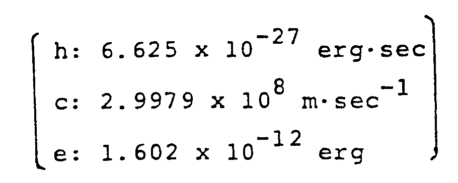
are substituted for the above equation, the wavelength λ having a unit in the order of angstroms and the charged voltage having a unit in the order of Kv, there is obtained an equation,

If the charged voltage has been known, therefore, the wavelength λmin can be easily calculated. For example, if the charged voltage Vmax is 24.8 Kv, there are generated electromagnetic waves over a wide range, the mininum wavelength thereof being 0.5 angstrom. However, the energy is not all converted. The conversion efficiency ε is given by,
where, - K:
- 1.1 x 10⁻⁹
- Z:
- atomic number of the atoms that received impingement
- I:
- discharge current
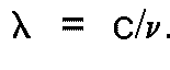
- With a semiconductor in which silicon forms the base, the electons move freely when they are irradiated with electromagnetic waves or a beam of particles having energy greater than an energy gap Eg (=1.2 eV). In terms of the threshold wavelength, the electrons move freely when they are irradiated with electromagnetic waves having wavelengths shorter than 10331.5 angstroms, since

region 102 in Fig. 9. - Thus, a metal part connected to the potential of the
active side 2 serves as an antenna which absorbs electromagnetic waves at the time when the static electricity sparks in compliance with the aforementioned equation
region 104 in Fig. 9). In a grounded circuit, the noise can be suppressed by the single-point grounding for the electromagnetic waves of up to the VHF band that is referred to in a radio communications system, and can be suppressed by the many-point grounding for the electromagnetic waves of the UHF band (region where waveguides are handled), which, however, are not omnipotent. That is, interference to the electronic devices caused by the static electricity must be eliminated by a method which does not rely upon the grounding circuit. The region based upon a new concept is indicated by 105 in Fig. 9. - Generally, electrically equivalent constants of a human body consist of a resistance of about one kiloohms and an electrostatic capacity of 200 pF to 500 pF. Fig. 10 shows electrostatic discharge characteristics for the amount of electric charge (Q) when the charged volatage (V) is 20 Kv, resistance (R) is 800 ohms, and electrostatic capacity (C) is 500 pF. The amount of electric charge (Q) is given by,

If the side in which the discharge takes place has zero resistance, a discharge time τ given by,
is required until the electric charge of 10 µC is discharged to 1/e. In practice, however, the side in which the discharge takes place has resistance to some extent, and a longer period of time is required for the discharge. If the electric charge passes through the CMOS IC in the electronic circuit network, the oxide film is completely destroyed (scattered). If the device is under the electrically charged condition in which the electric discharge does not take place, the potential of theactive side 2 is spread throughout the electronic circuit network that is constituted relying upon the idea of forming a grounding circuit. Therefore, erroneous input and erroneous operation caused by the electric charge take place on thepull side 3, in theinput line 4 and in the field-effect IC. - Harmful influences to the electronic devices caused by the static electricity are summarized below.
- (a) The patterns and metallic structural parts on the circuit board connected to the
active side 2 work as antennas depending upon the magnitude of energy of the static electricity, and absorb the electromagnetic waves to generate eddy currents which produce noise in the electronic circuit network. In particular, since the portable electronic devices cannot be ideally grounded, the energy of noise must be consumed in the electronic circuit network to form a factor of erroneous operation (region indicated by 103 in Fig. 9). - (b) The semiconductor in which silicon forms the base operates erroneously when it is irradiated with electromagnetic waves of a wavelength shorter than 10331.5 angstroms.
- (c) The device operates erroneously if the electric charge flows through the electronic circuit network, and the oxide film is broken (scattered) if the electric charge flows through the semiconductor.
- (d) The electronic circuit network is affected by the disturbance in the distribution of electric field in which the static electricity exists, when the electronic circuit network is provided with a field-effect IC which, in principle, is susceptible to the electric field.
- A semiconductor integrated circuit (IC) chip has many input/output terminals (hereinafter referred to as IC pads). The layout of IC pads will be discussed below.
Here, to simplify the description, the layout contains a minimum number of pads. Fig. 11 is a model diagram of the layout of IC pads that are mounted on a circuit board and are susceptible to the static electricity. Fig. 13 is is also a model diagram of the layout of IC pads that are mounted on a circuit board and are susceptible to the static electricity. Fig. 12 is a matrix diagram for comparing the positional relations related to the IC pad layout of Fig. 11, and Fig. 14 is a matrix diagram for comparing the positional relations related to the IC pad layout of Fig. 13. Names of coordinates of matrix are names of functions of IC pads. In Fig. 11, for example XIN and XOUT denote IC pads that constitute an oscillation circuit, and Ø₁ and Ø₂ denote IC pads that constitute a booster circuit. Symbol VDD denotes an IC pad which receives a potential of theactive side 2, and VSS denotes an IC pad which receives a potential of thepull side 3. Symbol SW denotes an IC pad of thecircuit 1 which is connected to an end of a switch in theinput line 4. As for the frames of XOUT and VSS on side of XIN in the matrix diagram of Fig. 12, symbol ○ is put to the frames of XOUT and VSS in the row of XIN and VSS. Next, as for XIN and SW on side of XOUT, symbol ○ is put to the frames of XIN and SW in the row of XOUT. Symbols ○ are put to the frames in the same manner as for Ø₁, and then as for Ø₂, SW, VDD and VSS, successively. Similarly, Fig. 14 is described based upon Fig. 13. Next, a diagram of Fig. 15 for comparing matrixes is described by combining the upper right portion of the diagonal line of the matrix diagram of Fig. 12 which shows the pads that are mounted on the circuit board and are susceptible to the static electricity with the lower left portion of the diagonal line of the matrix diagram of Fig. 14. In Fig. 15, symbols ○ that are located at symmetrical positions relative to the diagonal line are replaced by symbols ● . The matrix of symbols ● indicates that the layouts of IC pads of Figs. 11 and 13 are in a neighborhood relationship to each other. That is, XIN and XOUT, ø₁ and Ø₂, and VDD and SW indicate similar layouts having neighborhood relationship in Figs. 11 and 13. A diagram of Fig. 20 for comparing matrixes is described by combining the upper right portion of the diagonal line of the matrix diagram of Fig. 17 corresponding to Fig. 16 which shows the layout of IC pads that are mounted on the circuit board and are confirmed to be little affected by the static electricity, with the lower left portion of the diagonal line of a matrix diagram of Fig. 19 corresponding to Fig. 18 which shows the layout of IC pads that are confirmed to be little affected by the static electricity after they have been mounted. In Fig. 20, symbols ○ that are located at symmetrical positions relative to the diagonal line are replaced by symboles ● . The matrix of symbols ● indicates that the layouts of IC pads of Figs. 16 and 18 are in a neighborhood relationship to each other. That is, XIN and XOUT, Ø₁ and Ø₂, and VSS and SW indicate similar layouts having a neighborhood relationship in Figs. 15 and 17. - The IC that is easily affected by the static electricity after it has been mounted on the circuit board is compared below with the IC that is little affected, in regard to their similar points.

If similar points common to the easily affected IC and the little affected IC are eliminated, since they are irrelevant to whether they are little affected or easily affected, the following fact becomes obvious.
The results are discussed below. After mounted on the circuit board, the IC tends to be easily affected or little affected by the static electricity because of the reason that VDD (active side 2) has more patterns that stretch on the circuit board than VSS (pull side 3), since the circuit is designed based upon the idea of employing a grounding circuit. This fact is quite important to derive the following hypotheses. - The IC which is easily affected has VDD and SW (
active side 2 and input line 4) that are adjacent to each other. That is, there exists a large stray capacity Ca between theactive side 2 and theinput line 4. - The IC which is little affected has VSS and SW (pull
side 3 and input line 4) that are adjacent to each other. That is, a stray capacity Cp between thepull side 3 and theinput line 4 is smaller than the above-mentioned stray capacity Ca. - The following two examples will be described to prove the
hypotheses - Fig. 21 is a solid diagram of the circuit of a digital wristwatch, in which reference numeral 4a denotes a switch pattern which forms an end of the
input line active side 2. On theswitch pattern 4a is disposed theswitch spring 2b in an opposed manner over an area 9 of 10mm² maintaining a distance of 0.3 mm, to thereby form an air capacitor. Under this condition, the device is easily affected by the static electricity and operates erroneously for various control operations. If the shape of theswitch spring 2b is so changed that it is opposed to the switch pattern over anarea 10 instead of the area 9, then the device becomes little affected by the static electricity. This fact verifies theaforementioned hypothesis 1. As a follow-up experiment, a capacitor was inserted between theswitch pattern 4a and the potential VSS of thepull side 3 under the condition of the opposed area 9, in order to examine the immunity of the device against the static electricity. It was found that the device exhibited immunity if the capacitor had a capacity greater than a given value. Fig. 22 is a solid diagram showing another circuit of the electronic wristwatch. The device is little affected by the static electricity when a temporarily formed VDD pattern 11 is not provided on the VDD pattern 2b adjacent to theswitch pattern 4a, the VDD pattern 2b assuming the potential of theactive side 2. On the other hand, if the temporarily formed VDD pattern is located adjacent to theswitch pattern 4a as shown in the drawing, the device becomes susceptible to the static electricity and operates erroneously such as displaying incorrect indication. This is one of the verifications related to theaforementioned hypothesis 2. The idea to lengthen the pattern of theactive side 2 on the circuit board or to increase the area conforms to the way of thinking which is based upon the grounding circuit, but is not quite effective to suppress the noise that stems from the static electricity and rather makes the situation worse. - Even if the existing grounding circuit is employed in an attempt to cope with the static electricity, a discharge current of static electricity flows from the metal housing into the electronic circuit network, and the IC is broken down or electrical data in the circuit network are disturbed. Further, electromagnetic waves of large energy generated by lightning or the discharge of static electricity are absorbed by the metal housing and by the pattern of the
active side 2 to form eddy currents which then generate noise to disturb the electrical data in the electronic circuit network. Moreover, when the electronic device is placed under a condition where the static electricity is not discharged, the active side 2 (ground side) that spreads throughout the circuit board works more effectively to receive the static electricity than thepullside 3. Therefore, the electric field acts more greatly upon theactive side 2 than upon thepull side 3, and the device operates erroneously. - The present invention seeks to remove the above-mentioned defects and to provide an electronic device that has immunity against the phenomena of static electricity.
- According to the present invention, there is provided an electronic device having a power supply input circuit arranged for suppressing noise from static electricity, the input circuit comprising a first supply line arranged to be at a first source potential, a second supply line arranged to be at a second source potential, and an input line connected by way of a switch to the first supply line and by way of a resistance to the second supply line, said supply lines supplying power to a circuit of the device, characterised in that the first and second supply lines and the input line have a pattern layout of pads of an IC or leads on a circuit board for the input circuit such that a capacitance Ca between the first supply line and the input line and a capacitance Cp between the input line and the second supply line maintain a relation Ca < Cp.
- In a preferred embodiment of the present invention a metal housing of the device contains an input circuit which maintains an ordinary potential on the input line by inducing a pull potential on the input line in order to eliminate the induction of an active potential other than that for operating the device, thereby to prevent any erroneous input.
- Advantageously, furthermore, neither the active side (ground side) of the electronic circuit nor the electronic circuit network is permitted to be electrically connected to the housing in order to interrupt the flow of elecric charge and eddy currents produced by electro-magnetic waves of large energy. If the housing is made of an insulating material, this helps prevent the distribution of electric field from being disturbed in the electronic circuit, and makes it possible to achieve the desired object.
- The invention is described further by way of example, with reference to the accompanying drawings, in which:-
- Figure 1 is a diagram of a fundamental input circuit in an electronic circuit network according to the present invention;
- Figures 2 and 3 are diagrams of model layouts of IC pads according to the present invention;
- Figures 4 and 5 are diagrams illustrating portions of layouts of circuit board patterns according to the present invention;
- Figure 6 is a diagram illustrating an electronic circuit network and a metal housing according to the present invention;
- Figure 7 is a diagram which schematically illustrates the input circuit;
- Figure 8 is a diagram showing voltage waveforms of Figure 7;
- Figure 9 is a diagram to illustrate the concept related to the energy of electromagnetic waves and noise;
- Figure 10 is a diagram of waveforms which represent discharge characteristics of static electricity;
- Figures 11, 13, 16 and 18 are diagrams of layouts of IC pads for confirming the present invention;
- Figures 12, 14, 15, 17, 19 and 20 are matrix diagrams of IC pads for confirming the present invention; and
- Figures 21 and 22 are diagrams of circuit patterns for confirming the present invention.
- Figure 1 is a diagram of an input circuit according to an embodiment of the present invention, wherein Figure 1(a) is a diagram in which the
active side 2 assumes the higher potential of the power source voltage, and Figure 1(b) is a diagram in which theactive side 2 assumes the lower potential of the power source voltage.Reference numeral 1 denotes a circuit, 3 denotes a pull side, and 4 denotes an input line. An end of the input line is connected to a switch SW and the other end thereof is connected to the circuit. If the switch SW is turned on, the input line assumes the potential of theactive side 2 and if the switch SW is turned off, the input line assumes the potential of thepull side 3 via a pull resistance Rp. An electrostatic capacity between theactive side 2 and theinput line 4 is denoted by Ca and an electrostatic capacity between theinput line 4 and thepull side 3 is denoted by Cp, the electrostatic capacities having a relationship Ca < Cp. With the circuit being constructed as described above, even if an impulse is simultaneously superposed on theactive side 2 and on thepull side 3 that are power source lines, the potential of thepull side 3 appears on theinput line 4 via Cp due to the relationship Ca < Cp. Accordingly, the impulse noise is not induced on theinput line 4, and the circuit is prevented from operating erroneously. - Fig. 2 is a diagram of a model layout of IC pads illustrating important portions only according to a particular embodiment of the present invention, wherein Fig. 2(a) is a diagram of a layout of IC pads in a circuit structure in which the active side assumes the higher potential of the power source voltage, and Fig. 2(b) is a diagram of a layout of IC pads in a circuit structure in which the
active side 2 assumes the lower potential of the power source voltage. In Fig. 2(a), a terminal (for example, XIN in Figure) other than the pad of VDD, other than the pad of SW and other than the input pad for testing, is provided between the pad of VDD (active side 2) and the pad of SW (input line 4). That is, the device is so designed that the stray capacity is relatively decreased between theactive side 2 and theinput line 4. Namely, the capacity Ca is inevitably decreased in the pattern layout on the circuit board. In Fig. 2(b), a pad (for example, Ø₂ in Figure) other than the pad VSS or SW, and other than the input pad for testing is provided between the pad VSS (active side 2) and the pad SW (input line 4). That is, the device is so designed that the stray capacity is relatively decreased between theactive side 2 and theinput line 4. Namely, the capacity Ca is inevitably decreased in the pattern layout on the circuit board. - Fig. 3 is a diagram of a model layout of IC pads showing important portions only according to a further embodiment of the present invention, wherein Fig. 3(a) is a diagram of a layout of IC pads in a circuit structure in which the
active side 2 assumes the higher potential of the power source voltage, and Fig. 3(b) is a diagram of a layout of IC pads in a circuit structure in which theactive side 2 assumes the lower potential of the power source voltage. In Fig. 3(a), the pad SW (input line 4) is located adjacent to the pad VSS (pull side 3). That is, the device is so designed that the stray capacity is made as great as possible between thepull side 3 and theinput line 4. Namely, the capacity Cp is inevitably increased in the pattern layout on the circuit board. - Fig. 4 is a diagram showing a portion of the layout of circuit board patterns according to a still further embodiment of the present invention, wherein
reference numeral 2c denotes active pattern lines, 5 denotes a pattern other than the active pattern lines, other than the SW pattern lines and other than the pattern lines for testing. Symbols SW₁, SW₂ and SW₃ denote switch patterns, and reference numeral 6 denotes an IC chip. Thepattern 5 is formed between the active pattern lines 2ca and the pattern SW₃, so that the electrostatic capacity Ca is relatively decreased between theactive side 2 and the switch pattern SW₃ so as to realize the relationship Ca < Cp mentioned in Fig. 1. - Fig. 5 is a diagram showing a portion of the layout of circuit board patterns according to a yet further embodiment of the present invention, wherein
reference numeral 3a denotes pull pattern lines formed adjacent to SW₁ and SW₃ pattern lines. The electrostatic capacity Cp is relatively increased between thepull side 2 and the SW to achieve the relationship Ca < Cp mentioned with reference to Fig. 1. In any case, the layout is so designed that the relationship Ca < Cp is maintained in any portion of the pattern lines inclusive of, for example, through-holes. - Fig. 6 is a diagram showing the structure of an electronic device in which the
electronic circuit network 8 of the present invention illustrated in Figs. 1, 2, 3, 4 and 5 is contained in themetal housing 7 according to another embodiment of the present invention. Here, if the electrostatic discharge takes place with using themetal housing 7 as an electrode, the electric charge migrates by electric quantity stored in the metal housing due to the avlanche of electrons at the time of electric discharge. Here, however, themetal housing 7 is not electrically conducted to theelectronic circuit network 8, so that the electric charge will not flow into theelectronic circuit network 8. Simultaneously with the electric discharge, furthermore, the kinetic energy of electrons that have impinged upon themetal housing 7 is converted into electromagnetic waves of large energy, and whereby themetal housing 7 works as an antenna to absorb the electromagnetic waves that turn into eddy currents. According to this embodiment, however, the eddy currents are transformed into heat in themetal housing 7 and do not flow into theelectronic circuit network 8. - In practice, there are quite a few electronic devices that have the
metal housing 7 of the sealed structure. In most cases, therefore, the electromagnetic waves produced by the static electricity impinge directly onto theelectronic circuit network 8. According to the present invention, however, the electronic device is not adversely affected by the phenomena of static electricity owing to the relationship Ca < Cp which is the basis of the present invention. Namely, the embodiments of the present invention completely preclude advsese effects (a), (b), (c) and (d) caused by the static electricity from acting upon the electronic devices. - The present invention can be effectively adapted to electronic devices for medical uses and electronic devices to be mounted on aircraft that must not be affected by the phenomena of static electricity, lightning or the external electric field, as well as to electronic devices to be mounted on artificial satellites, for meteorological observations and for atomic utilization that are subject to be exposed to ionizing radiation, corpuscular radiation and charged particles. In the field of civil uses, the invention can be very effectively adapted to robots, IC cards, electronic computers, electronic measuring instruments, electronic cameras, electronic wristwatches and the like.
Claims (6)
- An electronic device having a power supply input circuit arranged for suppressing noise from static electricity, the input circuit comprising a first supply line (2) arranged to be at a first source potential, a second supply line (3) arranged to be at a second source potential, and an input line (4) connected by way of a switch (SW) to the first supply line and by way of a resistance (Rp) to the second supply line, said supply lines supplying power to a circuit (1) of the device, characterised in that the first and second supply lines and the input line have a pattern layout of pads of an IC or leads on a circuit board for the input circuit such that a capacitance Ca between the first supply line and the input line and a capacitance Cp between the input line and the second supply line maintain a relation Ca < Cp.
- An electronic device according to claim 1 characterised in that the relation Ca < Cp is maintained by the pattern layout of pads of an IC by providing between a pad for the first supply line (2) and a pad for the input line (4) a further pad other than the one for the first supply line (2), the one for the input line (4), and one for a test input.
- An electronic device according to claim 1 characterised in that the relation Ca < Cp is maintained by the pattern layout of pads of an IC by locating a pad for the second supply line (3) and a pad for the input line (4) adjacent to each other.
- An electronic device according to claim 1 characterised in that the relationship Ca < Cp is maintained by the pattern layout of leads on a circuit board by providing between a lead for the first supply line (2) and a lead for the input line (4) a lead other than the one for the first supply line (2), the one for the input line (4) and one for a test input line.
- An electronic device according to claim 1 characterised in that the relation Ca < Cp is maintained by the pattern layout of leads on a circuit board by locating a lead for the input line (4) adjacent to a lead for the second supply line (3).
- An electronic device according to any preceding claim characterised in that the input circuit is arranged in a metal housing (7), and in that the input circuit and the metal housing (7) are not electrically connected to each other.
Applications Claiming Priority (10)
| Application Number | Priority Date | Filing Date | Title |
|---|---|---|---|
| JP27036284 | 1984-12-21 | ||
| JP270362/84 | 1984-12-21 | ||
| JP25312085 | 1985-11-12 | ||
| JP253120/85 | 1985-11-12 | ||
| JP253119/85 | 1985-11-12 | ||
| JP25311985 | 1985-11-12 | ||
| JP25455385 | 1985-11-13 | ||
| JP254553/85 | 1985-11-13 | ||
| JP254552/85 | 1985-11-13 | ||
| JP25455285 | 1985-11-13 |
Publications (3)
| Publication Number | Publication Date |
|---|---|
| EP0243499A1 EP0243499A1 (en) | 1987-11-04 |
| EP0243499A4 EP0243499A4 (en) | 1989-12-28 |
| EP0243499B1 true EP0243499B1 (en) | 1993-05-19 |
Family
ID=27530254
Family Applications (1)
| Application Number | Title | Priority Date | Filing Date |
|---|---|---|---|
| EP86900257A Expired - Lifetime EP0243499B1 (en) | 1984-12-21 | 1985-12-20 | Electronic device having a power supply input circuit in which noise from static electricity is suppressed |
Country Status (5)
| Country | Link |
|---|---|
| US (1) | US4752862A (en) |
| EP (1) | EP0243499B1 (en) |
| JP (1) | JP2543688B2 (en) |
| DE (1) | DE3587356T2 (en) |
| WO (1) | WO1986003910A1 (en) |
Families Citing this family (5)
| Publication number | Priority date | Publication date | Assignee | Title |
|---|---|---|---|---|
| US5214562A (en) * | 1991-06-14 | 1993-05-25 | The United States Of America As Represented By The Secretary Of The Air Force | Electrostatic discharge protective circuit of shunting transistors |
| JP2770846B2 (en) | 1995-06-16 | 1998-07-02 | 日本電気株式会社 | FET switch circuit |
| US5717558A (en) * | 1995-11-30 | 1998-02-10 | Lucent Technologies Inc. | Electrostatic discharge protection for an electrical device |
| KR980010717A (en) * | 1996-07-24 | 1998-04-30 | 김광호 | How to prevent system malfunction caused by static electricity |
| JP2003256789A (en) * | 2002-02-26 | 2003-09-12 | Sony Corp | Memory device and memory storage device |
Family Cites Families (6)
| Publication number | Priority date | Publication date | Assignee | Title |
|---|---|---|---|---|
| JPS5135261A (en) * | 1974-09-20 | 1976-03-25 | Hitachi Ltd | |
| JPS5713811A (en) * | 1980-06-26 | 1982-01-23 | Mitsubishi Electric Corp | Processing system of input circuit |
| JPS5743453A (en) * | 1980-08-28 | 1982-03-11 | Nec Corp | Integrated circuit |
| US4557379A (en) * | 1983-12-16 | 1985-12-10 | Lane Container Company | Circuit board package and method of manufacture |
| US4617471A (en) * | 1983-12-27 | 1986-10-14 | Kabushiki Kaisha Toshiba | Image sensing device |
| US4580193A (en) * | 1985-01-14 | 1986-04-01 | International Business Machines Corporation | Chip to board bus connection |
-
1985
- 1985-12-20 EP EP86900257A patent/EP0243499B1/en not_active Expired - Lifetime
- 1985-12-20 JP JP61500420A patent/JP2543688B2/en not_active Expired - Fee Related
- 1985-12-20 DE DE8686900257T patent/DE3587356T2/en not_active Expired - Lifetime
- 1985-12-20 WO PCT/JP1985/000697 patent/WO1986003910A1/en not_active Ceased
- 1985-12-20 US US06/905,338 patent/US4752862A/en not_active Expired - Lifetime
Also Published As
| Publication number | Publication date |
|---|---|
| JP2543688B2 (en) | 1996-10-16 |
| EP0243499A4 (en) | 1989-12-28 |
| US4752862A (en) | 1988-06-21 |
| DE3587356T2 (en) | 1993-09-09 |
| EP0243499A1 (en) | 1987-11-04 |
| WO1986003910A1 (en) | 1986-07-03 |
| DE3587356D1 (en) | 1993-06-24 |
Similar Documents
| Publication | Publication Date | Title |
|---|---|---|
| US3676742A (en) | Means including a spark gap for protecting an integrated circuit from electrical discharge | |
| DE3264540D1 (en) | Device for protecting electronic circuits such as integrated circuits from electrostatic charges | |
| JPH04153096A (en) | Portable memory device | |
| EP0806835A3 (en) | Electronic component | |
| US4752862A (en) | Electronic device | |
| KR100426232B1 (en) | Electronic component and use of a protective structure contained therein | |
| US4942495A (en) | Electrostatic protection device for electronic cards | |
| RU2092932C1 (en) | Integrated circuit on semiconductor substrate | |
| KR940003158B1 (en) | Electronic device | |
| JPH0666404B2 (en) | Electronics | |
| JPWO1986003910A1 (en) | electronic equipment | |
| Ciarpi et al. | A 10 Gb/s line driver in 65 nm CMOS technology for radiation-pervaded and high-temperature applications | |
| US5214562A (en) | Electrostatic discharge protective circuit of shunting transistors | |
| JPH04311479A (en) | Method for protecting electronic part in circuit against radiation and protection device for said part | |
| KR100793148B1 (en) | Antistatic circuit of high frequency circuit with differential structure | |
| JP3474687B2 (en) | Earth pattern for lightning and static electricity protection | |
| JPS62191791A (en) | Noise-resistant structure of electronic apparatus | |
| JPS5915084Y2 (en) | solar power supply | |
| KR19980019226A (en) | ARRANGEMENT FOR SCREENING A MICROELECTRONIC CIRCUIT IN AN INTEGRATED CIRCUIT | |
| JPS6297896A (en) | Integrated circuit card | |
| JPS62204182A (en) | Electronic wrist watch | |
| JPS62221194A (en) | Electronics | |
| JPS62205698A (en) | Electronic equipment with anti-static structure | |
| Ki et al. | Dual-Sensor-Based Active Protector for Nuclear EMP and Prompt Gamma-Ray Detection | |
| Seidler et al. | The limits to hardening electronic boxes to IEMP coupling |
Legal Events
| Date | Code | Title | Description |
|---|---|---|---|
| PUAI | Public reference made under article 153(3) epc to a published international application that has entered the european phase |
Free format text: ORIGINAL CODE: 0009012 |
|
| 17P | Request for examination filed |
Effective date: 19861222 |
|
| AK | Designated contracting states |
Kind code of ref document: A1 Designated state(s): CH DE FR GB LI |
|
| A4 | Supplementary search report drawn up and despatched |
Effective date: 19891228 |
|
| 17Q | First examination report despatched |
Effective date: 19901122 |
|
| GRAA | (expected) grant |
Free format text: ORIGINAL CODE: 0009210 |
|
| AK | Designated contracting states |
Kind code of ref document: B1 Designated state(s): CH DE FR GB LI |
|
| REF | Corresponds to: |
Ref document number: 3587356 Country of ref document: DE Date of ref document: 19930624 |
|
| ET | Fr: translation filed | ||
| PLBE | No opposition filed within time limit |
Free format text: ORIGINAL CODE: 0009261 |
|
| STAA | Information on the status of an ep patent application or granted ep patent |
Free format text: STATUS: NO OPPOSITION FILED WITHIN TIME LIMIT |
|
| 26N | No opposition filed | ||
| REG | Reference to a national code |
Ref country code: GB Ref legal event code: IF02 |
|
| PGFP | Annual fee paid to national office [announced via postgrant information from national office to epo] |
Ref country code: FR Payment date: 20041208 Year of fee payment: 20 |
|
| PGFP | Annual fee paid to national office [announced via postgrant information from national office to epo] |
Ref country code: GB Payment date: 20041215 Year of fee payment: 20 |
|
| PGFP | Annual fee paid to national office [announced via postgrant information from national office to epo] |
Ref country code: DE Payment date: 20041216 Year of fee payment: 20 |
|
| PGFP | Annual fee paid to national office [announced via postgrant information from national office to epo] |
Ref country code: CH Payment date: 20041229 Year of fee payment: 20 |
|
| PG25 | Lapsed in a contracting state [announced via postgrant information from national office to epo] |
Ref country code: GB Free format text: LAPSE BECAUSE OF EXPIRATION OF PROTECTION Effective date: 20051219 |
|
| REG | Reference to a national code |
Ref country code: GB Ref legal event code: PE20 |
|
| REG | Reference to a national code |
Ref country code: CH Ref legal event code: PL |