EP0242295B1 - X-ray shielded electronic circuit box - Google Patents
X-ray shielded electronic circuit box Download PDFInfo
- Publication number
- EP0242295B1 EP0242295B1 EP87400850A EP87400850A EP0242295B1 EP 0242295 B1 EP0242295 B1 EP 0242295B1 EP 87400850 A EP87400850 A EP 87400850A EP 87400850 A EP87400850 A EP 87400850A EP 0242295 B1 EP0242295 B1 EP 0242295B1
- Authority
- EP
- European Patent Office
- Prior art keywords
- mechanical structure
- protective box
- box according
- metal
- protective
- Prior art date
- Legal status (The legal status is an assumption and is not a legal conclusion. Google has not performed a legal analysis and makes no representation as to the accuracy of the status listed.)
- Expired - Lifetime
Links
Images
Classifications
-
- G—PHYSICS
- G21—NUCLEAR PHYSICS; NUCLEAR ENGINEERING
- G21F—PROTECTION AGAINST X-RADIATION, GAMMA RADIATION, CORPUSCULAR RADIATION OR PARTICLE BOMBARDMENT; TREATING RADIOACTIVELY CONTAMINATED MATERIAL; DECONTAMINATION ARRANGEMENTS THEREFOR
- G21F1/00—Shielding characterised by the composition of the materials
- G21F1/02—Selection of uniform shielding materials
- G21F1/10—Organic substances; Dispersions in organic carriers
- G21F1/103—Dispersions in organic carriers
- G21F1/106—Dispersions in organic carriers metallic dispersions
-
- H—ELECTRICITY
- H01—ELECTRIC ELEMENTS
- H01L—SEMICONDUCTOR DEVICES NOT COVERED BY CLASS H10
- H01L23/00—Details of semiconductor or other solid state devices
- H01L23/552—Protection against radiation, e.g. light or electromagnetic waves
-
- H—ELECTRICITY
- H01—ELECTRIC ELEMENTS
- H01L—SEMICONDUCTOR DEVICES NOT COVERED BY CLASS H10
- H01L2924/00—Indexing scheme for arrangements or methods for connecting or disconnecting semiconductor or solid-state bodies as covered by H01L24/00
- H01L2924/0001—Technical content checked by a classifier
- H01L2924/0002—Not covered by any one of groups H01L24/00, H01L24/00 and H01L2224/00
Definitions
- the present invention relates to a protective housing for electronic circuits, hardened with respect to X-rays. It applies more particularly to protection against X-rays of high-performance electronic circuits used in the aeronautical and space fields.
- Efficient electronic circuits both in terms of processing speed and capacity, are very sensitive to the effects of X-rays; these effects can go as far as the destruction of the active components of the electronic circuits by passing through phenomena of interference and blocking (phenomenon of latch up in English terminology).
- a particularly important parameter is that of the period during which this quantity is delivered; the dose associated with its duration of application is called the dose rate.
- dose rate the dose associated with its duration of application.
- the behavior of the active components of electronic circuits at these parameters (dose, dose rate) and at the energy spectrum of this radiation is essentially linked to their manufacturing technology. In most cases, it is necessary to reduce the dose levels and dose rates to allow electronic circuits to maintain their functional integrity.
- One of the most widely used techniques for reducing the doses and dose rates received by electronic circuits is to enclose these circuits in a pure metal envelope of high atomic number.
- the metal and the thickness of the metal sheet are chosen and adapted according to the energy of the X-ray considered and the desired filtering rate. This metal sheet tends to provide effective protection against high doses and dose rates of X-rays.
- the need for protection can be felt from 10 to 300 Sv (1 to 10 krad) and from 103 to 105 Sv.s (105 107 rad.s).
- the metal sheet covers a metal structure, in particular a light alloy, containing the electronic circuits, this structure ensuring the function of mechanical resistance and protection.
- the metal sheet is mechanically attached to the entire outer surface of the metal structure.
- the metal sheet for protection against X-rays cannot be placed directly on all of the external faces of the metal structure of the encapsulation box because of the often complex profile thereof. This profile complexity is often imposed by heat dissipation constraints.
- the volume defined by the metal protective sheet is found to be greater than the volume of the mechanical structure to be protected. This leads to an increase in the weight and size of the mechanical structure, an increase reinforced by mechanical devices which become necessary for holding the metal sheet in place on the mechanical structure (spacers, brackets, screws, etc.). ). In addition, these devices holding must be made of the same metal as that of the protective metal sheet so as not to create "holes" in the protection against X-rays.
- Another technique consists in directly depositing metal for protection against X-rays on the mechanical structure to be protected, either by soaking the latter in a liquid bath, or by electrolysis. Unfortunately, these deposition methods are not possible for all the metals usable for protection against X-rays. In addition, there is always a need in this method to examine the corrosion compatibilities of the metals present.
- the thicknesses that can be deposited for metals suitable for this technique are limited, except to call into question the quality of adhesion of the deposit.
- obtaining a uniform deposit requires proceeding in successive stages with resumption of machining between the deposits in order to ensure, in certain cases, compliance with the dimensions of the encapsulation unit at the final stage.
- dielectric ceramics such as barium titanium or neodymium titanate, titanium oxide or a complex ceramic based on lead are cited.
- the proliferation of individual protections may prove to be more penalizing in weight than an overall protection of all the electronic components.
- the technology for developing the various materials constituting the stacks is based on processes used for the manufacture of capacitors and in particular sintering processes. In particular, the method described does not make it possible to obtain a material for protection against X-rays having a complex shape.
- the materials used consist mainly of a filler such as lead, dispersed in an organic binder.
- a filler such as lead
- Such protective materials are in particular described in document FR-A-2 190 717 filed in the name of the Giken Company, document FR-A-2 482 761 filed in the name of A. Maurin, and the patent US-A -3 622 432 from the HK PORTER Company.
- lead-based materials can only be used as X-ray protective material for low dose rate radiation associated with relatively long dose distribution times.
- the subject of the present invention is precisely a protective casing for electronic circuits, hardened with respect to X-rays, making it possible to remedy the various drawbacks given above.
- this protective casing allows, compared to the use of a heavy metal sheet covering a metallic structure, a significant gain in mass and bulk while ensuring effective protection against radiation of high dose rate. and in particular superior to those mentioned above.
- this protective casing does not pose any major manufacturing problem: it can be produced in a much shorter time than that necessary for the manufacture of the encapsulation casings of the prior art.
- the invention allows, with respect to document FR-A-2 547 113 cited above, an evolution of the protection levels X without affecting the definition of the electronic circuits contained in the housing.
- the invention relates to a protective housing for electronic circuits, hardened with respect to X-rays, characterized in that it comprises at least one element formed of a mechanical structure rigid composite material, consisting of a resin reinforced with fibers, and a material for protection against X-rays covering at least partially the mechanical structure, this protective material X being formed from a matrix of resin containing, in the form of a regularly dispersed powder, at least one metal and / or at least one inorganic compound of a metal, the powder melting only at a temperature at least equal to 630 ° C and the metal having a high atomic number , at least equal to 47.
- the powder may consist of a metal and an inorganic compound of this same metal or of another metal.
- This metal and this inorganic compound has a melting point greater than or equal to 630 ° C.
- Protection X must be associated with all of the visible faces of the box, taking into account the random direction of X-rays.
- a powder distributed regularly in a resin matrix leads to a loss of efficiency compared to the metal pure in sheet, all other conditions identical elsewhere.
- This loss of efficiency being essentially a function of the particle size of the powder and of the quantity of powder in the organic binder, a powder is preferably chosen having a particle size ranging from 0.5 to 25 ⁇ m, and for example ranging from 1, 6 to 10 ⁇ m.
- the amount of powder in the binder can range from 25 to 50% by volume of the finished material for protection against X-rays.
- the amount of doping of the organic binder in this range depends on the efficiency sought for protection X The same applies to the thickness of the X-ray protective material.
- the resin used to form the matrix of the protective material may be a thermoplastic or thermosetting resin whose coefficient of thermal expansion is compatible with that of the composite material forming the mechanical structure and whose polymerization catalyst is compatible with the resin of said composite material.
- resin used in the composition of the protective material X mention may, for example, be made of polyamides, polyethers, polyesters, phenoplasts, polyolefins, epoxides, polyimides, silicones, furans, etc.
- the metallic powder embedded in the organic matrix of the protective material X can be a powder of silver, antimony, barium, rare earth, tantalum, tungsten, rhenium, iridium, platinum, gold, uranium, hafnium or a mixture of these metals. Silver, tantalum, tungsten or uranium are preferably used.
- the powder when it consists of an inorganic component, it can be an oxide, a nitride or a heavy metal carbide such as those cited above.
- the inorganic compound is an oxide, a nitride, or a carbide of silver, tantalum, tungsten or uranium when this compound actually exists.
- one or more metals and / or one or more inorganic compounds of a metal can be used.
- the rigid mechanical structure is made of a material making it possible to withstand the mechanical stresses which the final protective casing must satisfy. It can be formed from a thermoplastic or thermosetting resin reinforced with fibers.
- thermosetting resins such as epoxy, phenolic, polyester, polyimide or furan resins are preferably used.
- the reinforcing fibers may be short or long and be made of an organic or inorganic material such as glass, carbon, boron, kevlar or metal.
- This composite material (resin + fibers) has a density ranging from 1.2 to 1.8 instead of 2.8 for aluminum.
- the weight gain of a rigid structure according to the invention is therefore significant.
- the mechanical structure has a shape and a size corresponding to the requirements for fixing and fitting the electronic circuits to be housed there. It is obtained by molding either by injection, by compression or by a hybrid technique called "compression-transfer molding" described in French patent application No. 85 18769 filed on December 18, 1985 in the name of the applicant.
- an overmolding of the material for protection against X-rays is carried out either by injection or by compression.
- the latter can be heated beforehand and / or be subjected to a surface preparation.
- This premix is carried out either by mixing the powder with molten grains of the resin and then by forming granules of mixture by extrusion, or by simple mixing of powders, or by mixing the powder in a liquid organic binder. This premix is then introduced into the mold to be polymerized on the mechanical structure.
- protective material X by overmolding ensures continuous and homogeneous adhesion of the material to the rigid mechanical structure. This makes it possible in particular to reduce the overall size of the encapsulation unit compared to the solutions of the prior art.
- the latter may be provided with notches formed during the molding of the structure. These notches are filled with the X-ray protective material during the overmolding of the latter, thus ensuring a desired additional hooking effect.
- the housing element may be covered with a material formed of at least one element with a low atomic number, at most equal to 6, constituting at least in part the external or internal surface of said housing element.
- This material has a thickness greater than the average free path of the electrons emitted by the walls of the case, protected against X-rays during X-ray irradiation. It always constitutes a coating of last layer towards the surrounding atmosphere.
- the material used to prevent these emissivity effects from the walls of the protective housing is generally known under the name of anti-SGEMP material (System Generating Electro Magnetic Pulse in English terminology). It can be in the form of a paint containing particles of the element with atomic number at most equal to 6. The paint is for example of the Pyroflex 7D 713 type from Astral.
- the element under consideration of the protective housing is equipped with a material which is a good conductor of electricity used to filter electromagnetic waves other than X-rays, this material covers either the external surface of the assembly formed by the mechanical structure and the protective material X and / or the internal surface of the mechanical structure.
- This material which is good conductor of electricity, constitutes a Faraday cage protecting the electronic circuits housed in the protective housing. It will be referred to hereinafter as "faradization" material.
- Beryllium has the advantage of being able to play both the role of anti-SGEMP material and the role of Faraday cage, given its low atomic number and good electrical conductivity.
- a protective housing formed of a one-piece cover fixed to a base in a single part, in which the element capable of being irradiated by X-radiation is the case; the possibilities of direction of the direction of the irradiation flux X are represented by the arrows F in FIGS. 1-3.
- the invention is of much more general application.
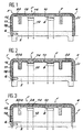
- FIG 1 there is shown schematically in longitudinal section an electronic circuit protection box comprising a base 2 on which is fixed a cover 4 for example using screws 6.
- This box is designed to receive the electronic circuits 8
- these circuits can be fixed by any known means to bosses 10 provided for this purpose on the internal face of the cover 4 of the housing.
- the electronic circuits 8 are connected to external electrical circuits to the housing, by conductive tracks shown diagrammatically at 12 and passing for example through the base 2 of the housing.
- the specific shape of the box, as well as the fixing and connection of the electronic circuits, housed in the X-ray protection box, are linked to the type of components used. Said components can be encapsulated in TO 5, TO 66 boxes, etc.
- the cover 4 comprises a rigid structure 14 ensuring the mechanical protection of the electronic circuits.
- This structure 14 is formed from a thermosetting plastic material such as bakelite, polyimide resins or silicones, reinforced with organic fibers or not.
- This structure 14 is for example made of KINEL 5504 sold by the company Rhône Poulenc, this material being a polyimide resin reinforced with long glass fibers, arranged randomly.
- This rigid structure 14 is formed by molding, either by injection or by compression, techniques well known to those skilled in the art. It can have a thickness of 2 mm.
- Protection against X-rays of electronic circuits 8 housed in the housing is ensured using a layer material 16 in contact with the internal surface of the rigid structure 14 or, as shown in the figure, in contact with the external surface of the rigid structure.
- the protective material 16 X covers the entire part of the external surface of the structure 14 capable of being irradiated by X-rays. In the case shown in FIG. 1, the layer of material 16 therefore covers the entire external surface of the structure 14, ie the upper face 15 and the lateral faces 17 of this structure.
- the latter can be equipped with notches 18, formed during the molding of the rigid structure 14. These notches 18 are filled with protective material X during the overmolding of the latter.
- the protective material 16 X is for example formed of a tungsten powder representing 30% by volume of the finished product, regularly dispersed, in a PA11 resin from ATOCHEM.
- This resin is a thermoplastic polyamide resin.
- the tungsten powder has an average particle size of 4 ⁇ m and a dispersion of 2.5. Its purity is 99.9%.
- This protective material can be obtained by melting granules of the resin PA11 to which the tungsten powder is added.
- the premix obtained is introduced into an extruder-granulator ZSK30 from the Werner Company in order to obtain granules of mixture which can then be introduced into a mold already containing the rigid structure 14 to be covered with the protective material X.
- the introduction of mixing granules in the mold is done by injection.
- the protective material X is overmolded on the heated rigid structure 14 in order to facilitate the adhesion of the material X.
- the protective material obtained may have a thickness of 1.5 mm.
- the molding and overmolding of the rigid structure 14 and of the protective material X, respectively, make it possible to directly obtain protective casing covers with the desired dimensions and precisions without resuming machining. Furthermore, these molding techniques are particularly advantageous from the financial point of view and manufacturing time since the series of casing covers to be produced make it possible to amortize the prices of specific tools of each case model.
- the protective material X can also consist of a powder containing 6% by volume of tungsten and 24% by volume of uranium oxide (UO2) embedded in the resin PA11. This material may have a thickness of 2 mm in order to ensure effective filtering.
- UO2 uranium oxide
- polyamide PA11 resin can be replaced by a polyetherblockamide resin.
- a resin is sold under the name DINYL from Rhône-Poulenc.
- the resin of the protective material 16 can also be made of bakelite or silicone.
- a material 20 anti-SGEMP forming the external surface of the cover 4 can be provided.
- this material 20 completely covers the protective material 16 X. It is made of beryllium thus ensuring, in addition to the anti-SGEMP function, the protection of the electronic circuits 8 against electromagnetic waves.
- the closure of the Faraday cage is obtained, for the case described here, by the presence of the base 2 made or covered with a metal which is a good conductor of electricity such as nickel, silver, aluminum, beryllium or copper.
- This material 20 must have a thickness greater than the mean free path of the electrons emitted by the walls of the cover. It also constitutes a top layer coating.
- the anti-SGEMP material advantageously constitutes the internal surface of the cover.
- FIG 2 there is shown a second embodiment of the protection device according to the invention.
- the material used to avoid the effects of emissivity of the walls of the housing subjected to X-rays, and in particular of the material 16, is made of a material 20a which is a poor conductor of electricity such as carbon or boron. . Under these conditions, the protection of the integrated circuits 8 against electromagnetic waves is not ensured.
- the internal surface of the rigid structure 14 is entirely covered with a layer 22 which is a good conductor of electricity.
- this layer 22 is made of a metal such as nickel or silver.
- This layer 22 has a thickness of approximately 0.1 mm.
- the other parts of the protective housing and in particular of the cover 4 are unchanged compared to the case of FIG. 1.
- FIG. 3 there is shown a third embodiment of the protective housing according to the invention. This embodiment differs from that of FIG. 2 only in that the layer playing the role of Faraday cage is disposed between the layer of anti-SGEMP material 20a and the layer of protective material 16 X.
- This layer 24 has a thickness of 0.1 mm and is made in particular of silver or nickel.
- the Faraday cage is closed by the presence of the base 2 made of metal or covered with a metal of good conductivity electric.
- the metallic "faradization" layer cannot be applied to a silicone surface, given the poor adhesion of such a metal to such a resin.
- the material for protection 16 against X-rays may cover only the upper face 15 of the mechanical structure or only the lateral faces 17 of this structure.
- the anti-SGEMP material 20 or 20a forming the external surface of the cover 4 of the housing, covers all of the protective material 16 X as well as the part of the rigid structure 14 not covered by the protective material 16 X
- a "faradization" layer can be interposed between the anti-SGEMP layer 20a and the parts of the external surface of the structure 14 not covered with material 16. protection X.
- the protection device according to the invention can be used wherever electronic circuits must be protected against X-rays. This protection can withstand severe mechanical and climatic environments. In particular, the invention applies when minimum mass conditions are required. Indeed, the protective casing according to the invention allows, with filtering efficiency equivalent to that of a sheet of solid material covering a metallic mechanical structure, a gain in mass, in bulk and a reduction in manufacturing costs. .
- the protective housing according to the invention can be advantageously used for the protection of high performance electronic devices, on board an aircraft.
Description
La présente invention a pour objet un boîtier de protection de circuits électroniques, durci vis-à-vis des rayons X. Elle s'applique plus spécialement à la protection contre les rayons X des circuits électroniques performants employés dans les domaines aéronautique et spatial.The present invention relates to a protective housing for electronic circuits, hardened with respect to X-rays. It applies more particularly to protection against X-rays of high-performance electronic circuits used in the aeronautical and space fields.
Les circuits électroniques performants, tant sur le plan de la vitesse de traitement que de la capacité, sont très sensibles aux effets des rayons X; ces effets peuvent aller jusqu'à la destruction des composants actifs des circuits électroniques en passant par des phénomènes de parasitage et de blocage (phénomène de latch up en terminologie anglo-saxonne).Efficient electronic circuits, both in terms of processing speed and capacity, are very sensitive to the effects of X-rays; these effects can go as far as the destruction of the active components of the electronic circuits by passing through phenomena of interference and blocking (phenomenon of latch up in English terminology).
En plus de la quantité ou dose de rayonnements X reçue, un paramètre particulièrement important est celui de la durée pendant laquelle cette quantité est délivrée; la dose associée à sa durée d'application est appelée le débit de dose. La tenue des composants actifs des circuits électroniques à ces paramètres (dose, débit de dose) et au spectre d'énergie de ce rayonnements est essentiellement liée à leur technologie de fabrication. Dans la plupart des cas, il est nécessaire de réduire les niveaux de dose et de débits de dose pour permettre aux circuits électroniques de garder leur intégrité fonctionnelle.In addition to the quantity or dose of X-rays received, a particularly important parameter is that of the period during which this quantity is delivered; the dose associated with its duration of application is called the dose rate. The behavior of the active components of electronic circuits at these parameters (dose, dose rate) and at the energy spectrum of this radiation is essentially linked to their manufacturing technology. In most cases, it is necessary to reduce the dose levels and dose rates to allow electronic circuits to maintain their functional integrity.
L'une des techniques les plus utilisées pour réduire les doses et débits de dose reçus par les circuits électroniques consiste à enfermer ces circuits dans une enveloppe de métal pur de numéro atomique élevé. Le métal et l'épaisseur de la feuille métallique sont choisis et adaptés en fonction de l'énergie du rayonnement X considéré et du taux de filtrage désiré. Cette feuille de métal tend à assurer une protection efficace contre les doses et débits de dose élevés de rayons X. Suivant les circuits et/ou la technologie des composants électroniques le besoin de protection peut se faire sentir partir de 10 à 300 Sv (1 à 10 krad) et de 10³ à 10⁵ Sv.s (10⁵ 10⁷ rad.s).One of the most widely used techniques for reducing the doses and dose rates received by electronic circuits is to enclose these circuits in a pure metal envelope of high atomic number. The metal and the thickness of the metal sheet are chosen and adapted according to the energy of the X-ray considered and the desired filtering rate. This metal sheet tends to provide effective protection against high doses and dose rates of X-rays. Depending on the circuits and / or the technology of the electronic components the need for protection can be felt from 10 to 300 Sv (1 to 10 krad) and from 10³ to 10⁵ Sv.s (10⁵ 10⁷ rad.s).
En général, la feuille métallique recouvre une structure en métal, notamment en alliage léger, renfermant les circuits électroniques, cette structure assurant la fonction de résistance et protection mécaniques. La feuille de métal est fixée sur toute la surface externe de la structure métallique de façon mécanique.In general, the metal sheet covers a metal structure, in particular a light alloy, containing the electronic circuits, this structure ensuring the function of mechanical resistance and protection. The metal sheet is mechanically attached to the entire outer surface of the metal structure.
Malheureusement, la mise en oeuvre des métaux les plus intéressants pour ce type de protection est difficile et coûteuse. Par ailleurs, les exigences vis-à-vis de ces matériaux de protection et la garantie de leur non dégradation vis-à-vis des diverses ambiances, climatiques, mécaniques, ionisantes, font que le devis de masse de l'ensemble des circuits électroniques est fortement augmenté par rapport aux circuits non protégés contre les rayons X.Unfortunately, the use of the most advantageous metals for this type of protection is difficult and costly. In addition, the requirements vis-à-vis these protective materials and the guarantee of their non-degradation vis-à-vis the various atmospheres, climatic, mechanical, ionizing, make that the mass estimate of all the electronic circuits is greatly increased compared to circuits not protected against X-rays.
Dans la plupart des cas, la feuille métallique de protection contre les rayons X ne peut être placée directement sur la totalité des faces extérieures de la structure métallique du boîtier d'encapsulation à cause du profil souvent complexe de celle-ci. Cette complexité de profil est souvent imposée par des contraintes de dissipation thermique.In most cases, the metal sheet for protection against X-rays cannot be placed directly on all of the external faces of the metal structure of the encapsulation box because of the often complex profile thereof. This profile complexity is often imposed by heat dissipation constraints.
En conséquence, le volume défini par la feuille de protection métallique se trouve être supérieur au volume de la structure mécanique à protéger. Ceci conduit à une augmentation du poids et de l'encombrement de la structure mécanique, augmentation renforcée par des dispositifs mécaniques qui deviennent nécessaires pour le maintien en place de la feuille métallique sur la structure mécanique (entretoises, équerres, visserie, etc...). En outre, ces dispositifs de maintien doivent être réalisés dans le même métal que celui de la feuille métallique de protection afin de ne pas créer de "trous" dans la protection contre les rayons X.Consequently, the volume defined by the metal protective sheet is found to be greater than the volume of the mechanical structure to be protected. This leads to an increase in the weight and size of the mechanical structure, an increase reinforced by mechanical devices which become necessary for holding the metal sheet in place on the mechanical structure (spacers, brackets, screws, etc.). ). In addition, these devices holding must be made of the same metal as that of the protective metal sheet so as not to create "holes" in the protection against X-rays.
Par ailleurs, le fait de réaliser la structure mécanique en métal ou en alliage augmente encore le poids total du boîtier d'encapsulation des circuits électroniques.Furthermore, the fact of making the mechanical structure of metal or alloy further increases the total weight of the encapsulation box for electronic circuits.
On conçoit que ces inconvénients d'encombrement et de poids des boîtiers d'encapsulation sont particulièrement gênants au niveau de l'emploi des circuits électroniques embarqués sur aéronef.It will be understood that these drawbacks of space and weight of the encapsulation boxes are particularly troublesome in terms of the use of electronic circuits on board aircraft.
Une autre technique consiste à effectuer directement le dépôt de métal de protection contre les rayons X sur la structure mécanique à protéger soit par trempage de celle-ci dans un bain liquide, soit par électrolyse. Malheureusement, ces procédés de dépôt ne sont pas possibles pour tous les métaux utilisables pour la protection contre les rayons X. De plus, il y a toujours lieu dans cette méthode d'examiner les compatibilités de corrosion des métaux en présence.Another technique consists in directly depositing metal for protection against X-rays on the mechanical structure to be protected, either by soaking the latter in a liquid bath, or by electrolysis. Unfortunately, these deposition methods are not possible for all the metals usable for protection against X-rays. In addition, there is always a need in this method to examine the corrosion compatibilities of the metals present.
D'autre part, les épaisseurs pouvant être déposées pour les métaux se prêtant à cette technique sont limitées, sauf à mettre en cause la qualité d'adhérence du dépôt. De plus, l'obtention de dépôt homogène impose de procéder par étapes successives avec reprise d'usinage entre les dépôts afin d'assurer, dans certains cas, le respect des cotes du boîtier d'encapsulation au stade final. Ces techniques de dépôt sont donc limitées et entraînent un coût élevé des boîtiers d'encapsulation protégés contre les rayons X.On the other hand, the thicknesses that can be deposited for metals suitable for this technique are limited, except to call into question the quality of adhesion of the deposit. In addition, obtaining a uniform deposit requires proceeding in successive stages with resumption of machining between the deposits in order to ensure, in certain cases, compliance with the dimensions of the encapsulation unit at the final stage. These deposition techniques are therefore limited and entail a high cost of the encapsulation boxes protected against X-rays.
Une autre approche consiste à envisager une protection spécifique pour chaque composant électronique embarqué, ceci constitue une solution différente et évoluée par rapport aux solutions classiques précédentes. Cette protection spécifique, décrite dans le document FR-A-2 547 113 déposé le 3 juin 1983, consiste à utiliser plusieurs couches empilées de matériaux différents ayant des numéros atomiques (Z) distincts.Another approach consists in considering a specific protection for each on-board electronic component, this constitutes a different and advanced solution compared to the previous conventional solutions. This specific protection, described in document FR-A-2 547 113 filed on June 3, 1983, consists in using several stacked layers of different materials having distinct atomic numbers (Z).
Comme matériau ayant un nombre de charge atomique élevé, il est cité des céramiques diélectriques telles que le titanate de baryum ou de néodyme, l'oxyde de titane ou encore une céramique complexe à base de plomb.As a material having a high atomic charge number, dielectric ceramics such as barium titanium or neodymium titanate, titanium oxide or a complex ceramic based on lead are cited.
Comme matériau ayant un nombre de charge atomique faible, il est cité le carbone, l'aluminium, le silicium, l'alumine et la silice.As a material having a low atomic charge number, carbon, aluminum, silicon, alumina and silica are cited.
Suivant les applications et le nombre de composants concernés, la multiplication des protections individuelles peut se révéler plus pénalisante en poids qu'une protection globale de l'ensemble des composants électroniques. Par ailleurs, la technologie d'élaboration des divers matériaux constituant les empilements s'appuie sur des procédés utilisés pour la fabrication de condensateurs et notamment de procédés de frittage. En particulier, le procédé décrit ne permet pas l'obtention d'un matériau de protection contre les rayons X ayant une forme complexe.Depending on the applications and the number of components concerned, the proliferation of individual protections may prove to be more penalizing in weight than an overall protection of all the electronic components. Furthermore, the technology for developing the various materials constituting the stacks is based on processes used for the manufacture of capacitors and in particular sintering processes. In particular, the method described does not make it possible to obtain a material for protection against X-rays having a complex shape.
Dans le cadre de la protection de personnes travaillant en présence de rayons X, les matériaux utilisés se composent principalement d'une charge telle que le plomb, dispersée dans un liant organique. De tels matériaux de protection sont en particulier décrits dans le document FR-A-2 190 717 déposé au nom de la Société Giken, le document FR-A-2 482 761 déposé au nom de A. Maurin, et le brevet US-A-3 622 432 de la H.K. PORTER Company.In the context of the protection of persons working in the presence of X-rays, the materials used consist mainly of a filler such as lead, dispersed in an organic binder. Such protective materials are in particular described in document FR-A-2 190 717 filed in the name of the Giken Company, document FR-A-2 482 761 filed in the name of A. Maurin, and the patent US-A -3 622 432 from the HK PORTER Company.
Ces matériaux à base de plomb ne peuvent être utilisés comme matériau de protection contre les rayons X que pour des rayonnements de faible débit de dose associé à des temps de distribution de la dose relativement importants.These lead-based materials can only be used as X-ray protective material for low dose rate radiation associated with relatively long dose distribution times.
Comme autre boîtier connu d'encapsulation de circuits électroniques, on peut citer celui décrit dans le document FR-A-2 490 917 déposé le 2 septembre 1980. Ce boîtier est constitué d'une matière plastique moulée telle qu'une résine époxyde dans laquelle sont noyés les circuits électroniques. Ce boîtier est extrêmement mince et ne permet pas d'assurer une protection mécanique efficace des circuits électroniques. Par ailleurs, aucune protection contre les rayons X n'est prévue.As another known case for encapsulating electronic circuits, mention may be made of that described in document FR-A-2 490 917 filed on September 2, 1980. This case consists of a molded plastic material such as an epoxy resin in which the electronic circuits are submerged. This case is extremely thin and does not provide effective mechanical protection for electronic circuits. Furthermore, no protection against X-rays is provided.
La présente invention a justement pour objet un boîtier de protection de circuits électroniques, durci vis-à-vis des rayons X, permettant de remédier aux différents inconvénients donnés ci-dessus. En particulier, ce boîtier de protection permet, par rapport à l'emploi d'une feuille de métal lourd recouvrant une structure métallique, un gain de masse et d'encombrement important tout en assurant une protection efficace contre les rayonnements de fort débit de dose et en particulier supérieurs à ceux cités plus avant.The subject of the present invention is precisely a protective casing for electronic circuits, hardened with respect to X-rays, making it possible to remedy the various drawbacks given above. In particular, this protective casing allows, compared to the use of a heavy metal sheet covering a metallic structure, a significant gain in mass and bulk while ensuring effective protection against radiation of high dose rate. and in particular superior to those mentioned above.
Par ailleurs, ce boîtier de protection ne pose pas de problème majeur de fabrication: il peut être réalisé en un temps beaucoup plus court que celui nécessaire pour la fabrication des boîtiers d'encapsulation de l'art antérieur.Furthermore, this protective casing does not pose any major manufacturing problem: it can be produced in a much shorter time than that necessary for the manufacture of the encapsulation casings of the prior art.
En outre, l'invention permet, par rapport au document FR-A-2 547 113 cité ci-dessus, une évolution des niveaux de protection X sans incidence sur la définition des circuits électroniques contenus dans le boîtier.In addition, the invention allows, with respect to document FR-A-2 547 113 cited above, an evolution of the protection levels X without affecting the definition of the electronic circuits contained in the housing.
De façon plus précise, l'invention a pour objet un boîtier de protection de circuits électroniques, durci vis-à-vis des rayons X, caractérisé en ce qu'il comprend au moins un élément formé d'une structure mécanique rigide en matériau composite, constitué d'une résine renforcée par des fibres, et d'un matériau de protection contre les rayons X recouvrant au moins en partie la structure mécanique, ce matériau de protection X étant formé d'une matrice en résine renfermant, sous forme d'une poudre régulièrement dispersée, au moins un métal et/ou au moins un composé inorganique d'un métal, la poudre ne fondant qu'à une température au moins égale à 630°C et le métal présentant un numéro atomique élevé, au moins égal à 47.More specifically, the invention relates to a protective housing for electronic circuits, hardened with respect to X-rays, characterized in that it comprises at least one element formed of a mechanical structure rigid composite material, consisting of a resin reinforced with fibers, and a material for protection against X-rays covering at least partially the mechanical structure, this protective material X being formed from a matrix of resin containing, in the form of a regularly dispersed powder, at least one metal and / or at least one inorganic compound of a metal, the powder melting only at a temperature at least equal to 630 ° C and the metal having a high atomic number , at least equal to 47.
En particulier, la poudre peut être constituée d'un métal et d'un composé inorganique de ce même métal ou d'un autre métal. Ce métal et ce composé inorganique présente une température de fusion supérieure ou égale à 630°C.In particular, the powder may consist of a metal and an inorganic compound of this same metal or of another metal. This metal and this inorganic compound has a melting point greater than or equal to 630 ° C.
Par élément du boîtier, il faut comprendre toute partie entrant dans la constitution du boîtier, telle que le capot, ou l'embase sur lequel est fixé le capot, ainsi qu'une partie du capot ou de l'embase (cas d'un capot ou d'une embase en plusieurs morceaux).By element of the housing, it is necessary to understand any part entering into the constitution of the housing, such as the cover, or the base on which the cover is fixed, as well as a part of the cover or the base (case of a hood or manifold in several pieces).
La protection X doit être associée à la totalité des faces apparentes du boîtier, compte tenu du sens aléatoire des rayonnements X.Protection X must be associated with all of the visible faces of the box, taking into account the random direction of X-rays.
L'utilisation de matériaux de température de fusion élevée permet d'éviter les effets indésirables dus aux chocs thermiques provoqués au sein du matériau lors d'une irradiation X, effets tels que la fusion superficielle des grains de la poudre pouvant conduire à la destruction du matériau de protection. En outre, l'utilisation d'un métal de numéro atomique élevé, supérieur ou égal à 47, permet un filtrage efficace des rayons X.The use of materials with a high melting temperature makes it possible to avoid the undesirable effects due to the thermal shocks caused within the material during X-ray irradiation, effects such as the surface melting of the grains of the powder which can lead to the destruction of the protective material. In addition, the use of a metal with a high atomic number, greater than or equal to 47, allows efficient filtering of X-rays.
A quantité de matériau égale, l'utilisation d'une poudre répartie régulièrement dans une matrice en résine amène une perte d'efficacité par rapport au métal pur en feuille, toutes autres conditions identiques par ailleurs. Cette perte d'efficacité étant fonction essentiellement de la granulométrie de la poudre et de la quantité de poudre dans le liant organique, on choisit de préférence une poudre présentant une granulométrie allant de 0,5 à 25 µm, et par exemple allant de 1,6 à 10 µm.For an equal amount of material, the use of a powder distributed regularly in a resin matrix leads to a loss of efficiency compared to the metal pure in sheet, all other conditions identical elsewhere. This loss of efficiency being essentially a function of the particle size of the powder and of the quantity of powder in the organic binder, a powder is preferably chosen having a particle size ranging from 0.5 to 25 μm, and for example ranging from 1, 6 to 10 µm.
De même, la quantité de poudre dans le liant peut aller de 25 à 50% en volume du matériau fini de protection contre les rayons X. La quantité de dopage du liant organique dans cette gamme est fonction de l'efficacité recherchée pour la protection X. Il en est de même pour l'épaisseur du matériau de protection contre les rayons X.Likewise, the amount of powder in the binder can range from 25 to 50% by volume of the finished material for protection against X-rays. The amount of doping of the organic binder in this range depends on the efficiency sought for protection X The same applies to the thickness of the X-ray protective material.
La résine utilisée pour former la matrice du matériau de protection peut être une résine thermoplastique ou thermodurcissable dont le coefficient de dilatation thermique est compatible avec celui du matériau composite formant la structure mécanique et dont le catalyseur de polymérisation est compatible avec la résine dudit matériau composite.The resin used to form the matrix of the protective material may be a thermoplastic or thermosetting resin whose coefficient of thermal expansion is compatible with that of the composite material forming the mechanical structure and whose polymerization catalyst is compatible with the resin of said composite material.
Comme résine entrant dans la composition du matériau de protection X, on peut par exemple citer les polyamides, les polyéthers, les polyesters, les phénoplastes, les polyoléfines, les époxydes, les polyimides, les silicones, les furaniques, etc.As resin used in the composition of the protective material X, mention may, for example, be made of polyamides, polyethers, polyesters, phenoplasts, polyolefins, epoxides, polyimides, silicones, furans, etc.
La poudre métallique noyée dans la matrice organique du matériau de protection X peut être une poudre d'argent, d'antimoine, de baryum, d'une terre rare, de tantale, de tungstène, de rhénium, d'iridium, de platine, d'or, d'uranium, d'hafnium ou un mélange de ces métaux. On utilise de préférence l'argent, le tantale, le tungstène ou l'uranium.The metallic powder embedded in the organic matrix of the protective material X can be a powder of silver, antimony, barium, rare earth, tantalum, tungsten, rhenium, iridium, platinum, gold, uranium, hafnium or a mixture of these metals. Silver, tantalum, tungsten or uranium are preferably used.
Lorsque la poudre est constituée d'un composant inorganique, celle-ci peut être un oxyde, un nitrure ou un carbure d'un métal lourd tels que ceux cités ci-dessus. En particulier, le composé inorganique est un oxyde, un nitrure, ou un carbure d'argent, de tantale, de tungstène ou d'uranium lorsque ce composé existe effectivement.When the powder consists of an inorganic component, it can be an oxide, a nitride or a heavy metal carbide such as those cited above. In particular, the inorganic compound is an oxide, a nitride, or a carbide of silver, tantalum, tungsten or uranium when this compound actually exists.
Afin d'optimiser la protection contre les rayons X sur un spectre d'énergie très étendue, on peut utiliser un ou plusieurs métaux et/ou un ou plusieurs composés inorganiques d'un métal.In order to optimize protection against X-rays over a very wide energy spectrum, one or more metals and / or one or more inorganic compounds of a metal can be used.
La structure mécanique rigide est constituée en un matériau permettant de supporter les contraintes mécaniques auxquelles le boîtier de protection final doit satisfaire. Elle peut être formée à partir d'une résine thermoplastique ou thermodurcissable renforcée par des fibres.The rigid mechanical structure is made of a material making it possible to withstand the mechanical stresses which the final protective casing must satisfy. It can be formed from a thermoplastic or thermosetting resin reinforced with fibers.
Toutefois, afin d'assurer une excellente résistance mécanique, on utilise de préférence des résines thermodurcissables telles que des résines époxydes, phénoliques, polyesters, polyimides, furaniques. Les fibres de renfort peuvent être courtes ou longues et être réalisées en un matériau organique ou inorganique tel que le verre, le carbone, le bore, le kevlar ou en métal.However, in order to ensure excellent mechanical resistance, thermosetting resins such as epoxy, phenolic, polyester, polyimide or furan resins are preferably used. The reinforcing fibers may be short or long and be made of an organic or inorganic material such as glass, carbon, boron, kevlar or metal.
Ce matériau composite (résine + fibres) présente une densité allant de 1,2 à 1,8 au lieu de 2,8 pour l'aluminium. Le gain en poids d'une structure rigide selon l'invention est donc important.This composite material (resin + fibers) has a density ranging from 1.2 to 1.8 instead of 2.8 for aluminum. The weight gain of a rigid structure according to the invention is therefore significant.
La structure mécanique présente une forme et un dimensionnement correspondant aux besoins de fixation et d'aménagement des circuits électroniques devant y être logés. Elle est obtenue par moulage soit par injection, soit par compression ou soit par une technique hybride dite "moulage par compression-transfert" décrite dans la demande de brevet français n° 85 18769 déposée le 18 décembre 1985 au nom du demandeur.The mechanical structure has a shape and a size corresponding to the requirements for fixing and fitting the electronic circuits to be housed there. It is obtained by molding either by injection, by compression or by a hybrid technique called "compression-transfer molding" described in French patent application No. 85 18769 filed on December 18, 1985 in the name of the applicant.
Sur la structure rigide ainsi obtenue, on effectue un surmoulage du matériau de protection contre les rayons X soit par injection, soit par compression. Afin d'assurer une bonne adhérence du matériau de protection X sur la structure mécanique, cette dernière peut être préalablement chauffée et/ou faire l'objet d'une préparation de surface.On the rigid structure thus obtained, an overmolding of the material for protection against X-rays is carried out either by injection or by compression. In order to ensure good adhesion of the protective material X to the mechanical structure, the latter can be heated beforehand and / or be subjected to a surface preparation.
Afin d'obtenir une bonne répartition de la poudre dans le liant organique, formant le matériau de protection contre les rayons X, gage d'une homogénéité de l'opacité, on effectue avant le surmoulage un prémélange de la poudre et du liant.In order to obtain a good distribution of the powder in the organic binder, forming the material for protection against X-rays, which guarantees homogeneity of the opacity, a premixing of the powder and the binder is carried out before overmolding.
Ce prémélange est effectué soit en mélangeant la poudre à des grains fondus de la résine puis en formant des granulés de mélange par extrusion, soit par simple mélange de poudres, soit par mélange de la poudre dans un liant organique liquide. Ce prémélange est ensuite introduit dans le moule pour être polymérisé sur la structure mécanique.This premix is carried out either by mixing the powder with molten grains of the resin and then by forming granules of mixture by extrusion, or by simple mixing of powders, or by mixing the powder in a liquid organic binder. This premix is then introduced into the mold to be polymerized on the mechanical structure.
La réalisation du matériau de protection X par surmoulage permet d'assurer une adhérence continue et homogène du matériau sur la structure mécanique rigide. Ceci permet notamment de réduire l'encombrement global du boîtier d'encapsulation par rapport aux solutions de l'art antérieur.The production of protective material X by overmolding ensures continuous and homogeneous adhesion of the material to the rigid mechanical structure. This makes it possible in particular to reduce the overall size of the encapsulation unit compared to the solutions of the prior art.
Afin d'améliorer l'accrochage du matériau de protection contre les rayons X sur la structure rigide mécanique, celle-ci peut être munie d'encoches, formées lors du moulage de la structure. Ces encoches se remplissent du matériau de protection contre les rayons X lors du surmoulage de ce dernier, assurant ainsi un effet d'accrochage supplémentaire recherché.In order to improve the attachment of the X-ray protective material to the rigid mechanical structure, the latter may be provided with notches formed during the molding of the structure. These notches are filled with the X-ray protective material during the overmolding of the latter, thus ensuring a desired additional hooking effect.
Afin d'éviter l'émission d'électrons par les parois ou éléments du boîtier de protection lors d'une irradiation X et en particulier par la poudre métallique, l'élément de boîtier peut être recouvert d'un matériau formé d'au moins un élément de numéro atomique faible, au plus égal à 6, constituant au moins en partie la surface externe ou interne dudit élément de boîtier.In order to avoid the emission of electrons from the walls or elements of the protective housing during X-ray irradiation and in particular by metallic powder, the housing element may be covered with a material formed of at least one element with a low atomic number, at most equal to 6, constituting at least in part the external or internal surface of said housing element.
Ce matériau présente une épaisseur supérieure au libre parcours moyen des électrons émis par les parois du boîtier protégées contre les rayons X, lors de l'irradiation X. Il constitue toujours un revêtement de dernière couche vers l'atmosphère environnante.This material has a thickness greater than the average free path of the electrons emitted by the walls of the case, protected against X-rays during X-ray irradiation. It always constitutes a coating of last layer towards the surrounding atmosphere.
Comme élément de numéro atomique faible on peut citer le carbone, le bore, et le béryllium.As an element with a low atomic number, mention may be made of carbon, boron, and beryllium.
Le matériau servant empêcher ces effets d'émissivité des parois du boîtier de protection est généralement connu sous le nom de matériau anti-SGEMP (System Generating Electro Magnetic Pulse en terminologie anglo-saxonne). Il peut se présenter sous la forme d'une peinture renfermant des particules de l'élément de numéro atomique au plus égale à 6. La peinture est par exemple de type Pyroflex 7D 713 d'Astral.The material used to prevent these emissivity effects from the walls of the protective housing is generally known under the name of anti-SGEMP material (System Generating Electro Magnetic Pulse in English terminology). It can be in the form of a paint containing particles of the element with atomic number at most equal to 6. The paint is for example of the Pyroflex 7D 713 type from Astral.
De façon avantageuse, l'élément considéré du boîtier de protection est équipé d'un matériau bon conducteur de l'électricité servant à filtrer les ondes électromagnétiques autres que les rayons X, ce matériau recouvre soit la surface externe de l'ensemble formé par la structure mécanique et le matériau de protection X et/ou la surface interne de la structure mécanique.Advantageously, the element under consideration of the protective housing is equipped with a material which is a good conductor of electricity used to filter electromagnetic waves other than X-rays, this material covers either the external surface of the assembly formed by the mechanical structure and the protective material X and / or the internal surface of the mechanical structure.
Ce matériau bon conducteur de l'électricité constitue une cage de Faraday protégeant les circuits électroniques logés dans le boîtier de protection. Il sera dénommé ci-après matériau de "faradisation".This material, which is good conductor of electricity, constitutes a Faraday cage protecting the electronic circuits housed in the protective housing. It will be referred to hereinafter as "faradization" material.
Comme matériau de "faradisation" on peut citer le nickel, l'argent, l'aluminium pur, le cuivre et le béryllium.As faradization material, nickel, silver, pure aluminum, copper and beryllium can be mentioned.
Le béryllium a l'avantage de pouvoir jouer à la fois le rôle de matériau anti-SGEMP et le rôle de cage de Faraday, compte tenu de son faible numéro atomique et de sa bonne conductivité électrique.Beryllium has the advantage of being able to play both the role of anti-SGEMP material and the role of Faraday cage, given its low atomic number and good electrical conductivity.
D'autres caractéristiques et avantages de l'invention ressortiront mieux de la description qui va suivre donnée à titre illustratif et non limitatif, en référence aux figures annexées, dans lesquelles:
- la figure 1 représente schématiquement, en coupe longitudinale, un premier mode de réalisation du dispositif de protection selon l'invention,
- la figure 2 représente schématiquement, en coupe longitudinale, un second mode de réalisation du boîtier de protection selon l'invention, et
- la figure 3 représente schématiquement, en coupe longitudinale, un troisième mode de réalisation du boîtier de protection selon l'invention.
- FIG. 1 schematically represents, in longitudinal section, a first embodiment of the protection device according to the invention,
- FIG. 2 schematically represents, in longitudinal section, a second embodiment of the protective housing according to the invention, and
- Figure 3 shows schematically, in longitudinal section, a third embodiment of the protective housing according to the invention.
En vue d'une simplification de la description, celle-ci se réfère à un boîtier de protection, formé d'un capot monobloc fixé sur une embase en une seule partie, dans lequel l'élément susceptible d'être irradié par un rayonnement X est le boîtier; les possibilités de direction du sens du flux d'irradiation X sont représentées par les flèches F sur les figures 1-3. Bien entendu, comme donné précédemment, l'invention est d'application beaucoup plus générale.In order to simplify the description, it refers to a protective housing, formed of a one-piece cover fixed to a base in a single part, in which the element capable of being irradiated by X-radiation is the case; the possibilities of direction of the direction of the irradiation flux X are represented by the arrows F in FIGS. 1-3. Of course, as given above, the invention is of much more general application.
Sur la figure 1, on a schématisé en coupe longitudinale un boîtier de protection de circuits électroniques comportant une embase 2 sur laquelle vient se fixer un capot 4 par exemple à l'aide de vis 6. Ce boîtier est prévu pour recevoir les circuits électroniques 8. En particulier, ces circuits peuvent être fixés par tout moyen connu sur des bossages 10 prévus à cet effet sur la face interne du capot 4 du boîtier. De manière très schématique, n'étant pas l'objet de la présente demande de brevet, les circuits électroniques 8 sont connectés à des circuits électriques, extérieurs au boîtier, par des pistes conductrices schématisées en 12 et traversant par exemple l'embase 2 du boîtier.In Figure 1, there is shown schematically in longitudinal section an electronic circuit protection box comprising a
La forme spécifique du boîtier, ainsi que la fixation et la connexion des circuits électroniques, logés dans le boîtier de protection contre les rayonnements X, sont liées au type de composants utilisés. Lesdits composants peuvent être encapsulés dans des boîtiers TO 5, TO 66, etc...The specific shape of the box, as well as the fixing and connection of the electronic circuits, housed in the X-ray protection box, are linked to the type of components used. Said components can be encapsulated in TO 5, TO 66 boxes, etc.
Selon l'invention, le capot 4 comporte une structure rigide 14 assurant la protection mécanique des circuits électroniques. Cette structure 14 est formée d'une matière plastique thermodurcissable telle que la bakélite, les résines polyimides ou les silicones, renforcée par des fibres organiques ou non. Cette structure 14 est par exemple réalisée en KINEL 5504 commercialisée par la Société Rhône Poulenc, ce matériau étant une résine polyimide renforcée par des fibres de verre longues, disposées de manière aléatoire. Cette structure rigide 14 est formée par moulage, soit par injection, soit par compression, techniques bien connues de l'homme du métier. Elle peut présenter une épaisseur de 2 mm.According to the invention, the cover 4 comprises a
La protection contre les rayons X des circuits électroniques 8 logés dans le boîtier est assurée à l'aide d'un matériau en couche 16 en contact avec la surface interne de la structure rigide 14 ou, comme représenté sur la figure, en contact avec la surface externe de la structure rigide.Protection against X-rays of
Le matériau 16 de protection X recouvre toute la partie de la surface externe de la structure 14 susceptible d'être irradiée par des rayonnements X. Dans le cas représenté sur la figure 1, la couche de matériau 16 recouvre donc toute la surface externe de la structure 14, soit la face supérieure 15 et les faces latérales 17 de cette structure.The protective material 16 X covers the entire part of the external surface of the
Afin d'assurer une bonne adhérence du matériau de protection 16 sur la structure rigide 14, cette dernière peut être équipée d'encoches 18, formées lors du moulage de la structure rigide 14. Ces encoches 18 sont remplies de matériau de protection X lors du surmoulage de ce dernier.In order to ensure good adhesion of the
Le matériau 16 de protection X est par exemple formé d'une poudre de tungstène représentant 30% en volume du produit fini, régulièrement dispersée, dans une résine PA11 de chez ATOCHEM. Cette résine est une résine polyamide thermoplastique. La poudre de tungstène présente une granulométrie moyenne de 4 µm et une dispersion de 2,5. Sa pureté est de 99,9%.The protective material 16 X is for example formed of a tungsten powder representing 30% by volume of the finished product, regularly dispersed, in a PA11 resin from ATOCHEM. This resin is a thermoplastic polyamide resin. The tungsten powder has an average particle size of 4 µm and a dispersion of 2.5. Its purity is 99.9%.
Ce matériau de protection peut être obtenu par fusion de granulés de la résine PA11 auxquels on ajoute la poudre de tungstène. Le prémélange obtenu est introduit dans une extrudeuse-granuleuse ZSK30 de la Société Werner afin d'obtenir des granulés de mélange qui peuvent être ensuite introduits dans un moule contenant déjà la structure rigide 14 à recouvrir par le matériau de protection X. L'introduction des granulés de mélange dans le moule se fait par injection. Le surmoulage du matériau de protection X est assuré sur la structure rigide 14 chauffée afin de faciliter l'adhérence du matériau X. Le matériau de protection obtenu peut présenter une épaisseur de 1,5 mm.This protective material can be obtained by melting granules of the resin PA11 to which the tungsten powder is added. The premix obtained is introduced into an extruder-granulator ZSK30 from the Werner Company in order to obtain granules of mixture which can then be introduced into a mold already containing the
Le moulage et le surmoulage respectivement de la structure rigide 14 et du matériau 16 de protection X permettent d'obtenir directement des capots de boîtiers de protection aux dimensions et précisions souhaitées sans reprise d'usinage. Par ailleurs, ces techniques de moulage sont particulièrement avantageuses du point de vue financier et temps de fabrication dès lors que les séries de capots de boîtiers à réaliser permettent d'amortir les prix des outillages spécifiques de chaque modèle de boîtier.The molding and overmolding of the
Le matériau de protection X peut aussi être constitué d'une poudre contenant 6% en volume de tungstène et 24% en volume d'oxyde d'uranium (UO₂) noyé dans la résine PA11. Ce matériau peut présenter une épaisseur de 2 mm afin d'assurer un filtrage efficace.The protective material X can also consist of a powder containing 6% by volume of tungsten and 24% by volume of uranium oxide (UO₂) embedded in the resin PA11. This material may have a thickness of 2 mm in order to ensure effective filtering.
De même, la résine polyamide PA11 peut être remplacée par une résine polyétherblockamide. Une telle résine est commercialisée sous le nom de DINYL de chez Rhône-Poulenc. La résine du matériau de protection 16 peut encore être en bakélite ou en silicone.Similarly, the polyamide PA11 resin can be replaced by a polyetherblockamide resin. Such a resin is sold under the name DINYL from Rhône-Poulenc. The resin of the
Afin d'éviter le renforcement du niveau électromagnétique dû à l'émission d'électrons par les parois extérieures du boîtier de protection, lors d'une irradiation X, et en particulier par le métal contenu dans le matériau 16 de protection X, un matériau 20 anti-SGEMP formant la surface externe du capot 4 peut être prévu. Dans le cas représenté sur la figure 1, ce matériau 20 recouvre totalement le matériau 16 de protection X. Il est réalisé en béryllium assurant ainsi en plus de la fonction anti-SGEMP, la protection des circuits électroniques 8 contre les ondes électromagnétiques.In order to avoid the reinforcement of the electromagnetic level due to the emission of electrons by the external walls of the protective housing, during X-ray irradiation, and in particular by the metal contained in the protective material X, a
La fermeture de la cage de Faraday est obtenue, pour le cas décrit ici, par la présence de l'embase 2 réalisée ou recouverte en un métal bon conducteur de l'électricité tel que le nickel, l'argent, l'aluminium, le béryllium ou le cuivre.The closure of the Faraday cage is obtained, for the case described here, by the presence of the
Ce matériau 20 doit présenter une épaisseur supérieure au libre parcours moyen des électrons émis par les parois du capot. Il constitue en outre un revêtement de dernière couche. En particulier, dans le cas d'un matériau de protection X recouvrant la surface interne de la structure mécanique, le matériau anti-SGEMP constitue avantageusement la surface interne du capot.This
Il est possible d'envisager l'emploi simultané d'une couche anti-SGEMP constituant la surface interne du boîtier et d'une couche anti-SGEMP constituant la surface externe du boîtier.It is possible to envisage the simultaneous use of an anti-SGEMP layer constituting the internal surface of the housing and an anti-SGEMP layer constituting the external surface of the housing.
Sur la figure 2, on a représenté un second mode de réalisation du dispositif de protection selon l'invention. Dans ce mode de réalisation, le matériau servant à éviter les effets d'émissivité des parois du boîtier soumises aux rayons X, et en particulier du matériau 16, est réalisé en un matériau 20a mauvais conducteur de l'électricité comme le carbone ou le bore. Dans ces conditions, la protection des circuits intégrés 8 contre les ondes électromagnétiques n'est pas assurée.In Figure 2, there is shown a second embodiment of the protection device according to the invention. In this embodiment, the material used to avoid the effects of emissivity of the walls of the housing subjected to X-rays, and in particular of the
Afin d'assurer cette protection, la surface interne de la structure rigide 14 est recouverte en totalité d'une couche 22 bonne conductrice de l'électricité. En particulier cette couche 22 est réalisée en un métal tel que le nickel ou l'argent. Cette couche 22 présente une épaisseur d'environ 0,1 mm. Les autres parties du boîtier de protection et en particulier du capot 4 sont inchangées par rapport au cas de la figure 1.In order to ensure this protection, the internal surface of the
Sur la figure 3, on a représenté un troisième mode de réalisation du boîtier de protection selon l'invention. Ce mode de réalisation ne diffère de celui de la figure 2 que par le fait que la couche jouant le rôle de cage de Faraday est disposée entre la couche de matériau anti-SGEMP 20a et la couche de matériau 16 de protection X. Cette couche 24 présente une épaisseur de 0,1 mm et est réalisée notamment en argent ou en nickel.In Figure 3, there is shown a third embodiment of the protective housing according to the invention. This embodiment differs from that of FIG. 2 only in that the layer playing the role of Faraday cage is disposed between the layer of
Comme dans le cas de la figure 1, la cage de Faraday est fermée par la présence de l'embase 2 réalisée en métal ou recouverte d'un métal de bonne conductivité électrique.As in the case of FIG. 1, the Faraday cage is closed by the presence of the
En vue de simplifier la fabrication du boîtier de protection selon l'invention et d'assurer une bonne isolation des circuits électroniques 8 contre les ondes électromagnétiques, il est possible de prévoir une couche de "faradisation" 22-24 recouvrant à la fois la face interne de la structure mécanique 14 (figure 2) et la surface externe du matériau de protection 16 contre les rayons X (figure 3). Ceci peut être réalisé par simple trempage de la structure mécanique 14, revêtue du matériau de protection 16, dans un bain contenant le métal à déposer pour jouer le rôle de cage de Faraday (dépôt chimique).In order to simplify the manufacture of the protective housing according to the invention and to ensure good insulation of the
Il est à noter que la couche métallique de "faradisation" ne peut pas être appliquée sur une surface en silicone compte tenu de la mauvaise adhérence, d'un tel métal sur une telle résine.It should be noted that the metallic "faradization" layer cannot be applied to a silicone surface, given the poor adhesion of such a metal to such a resin.
La description donnée précédemment n'a bien entendu été donnée qu'à titre illustratif, des modifications, sans pour autant sortir du cadre de l'invention, pouvant être envisagées. En particulier, le matériau de protection 16 contre les rayons X peut ne recouvrir que la face supérieure 15 de la structure mécanique ou que les faces latérales 17 de cette structure. Dans ce cas, le matériau anti-SGEMP 20 ou 20a, formant la surface externe du capot 4 du boîtier, recouvre la totalité du matériau 16 de protection X ainsi que la partie de la structure rigide 14 non recouverte par le matériau 16 de protection X. En outre, lorsque le matériau anti-SGEMP est mauvais conducteur de l'électricité, une couche de "faradisation" peut être intercalée entre la couche anti-SGEMP 20a et les parties de la surface externe de la structure 14 non recouvertes de matériau 16 de protection X.The description given above has of course been given only by way of illustration, modifications, without departing from the scope of the invention, which can be envisaged. In particular, the material for
Le dispositif de protection selon l'invention peut être utilisé partout où des circuits électroniques doivent être protégés contre les rayons X. Cette protection permet de supporter des ambiances mécaniques, climatiques sévères. En particulier, l'invention s'applique lorsqu'il est requis des conditions de masse minimum. En effet, le boîtier de protection selon l'invention permet, à efficacité de filtrage équivalente à celle d'une feuille en matériau massif recouvrant une structure mécanique métallique,un gain de masse, d'encombrement ainsi qu'une diminution des coûts de fabrication.The protection device according to the invention can be used wherever electronic circuits must be protected against X-rays. This protection can withstand severe mechanical and climatic environments. In particular, the invention applies when minimum mass conditions are required. Indeed, the protective casing according to the invention allows, with filtering efficiency equivalent to that of a sheet of solid material covering a metallic mechanical structure, a gain in mass, in bulk and a reduction in manufacturing costs. .
Ainsi, le boîtier de protection selon l'invention peut être utilisé avantageusement pour la protection de dispositifs électroniques très performants, embarqués sur aéronef.Thus, the protective housing according to the invention can be advantageously used for the protection of high performance electronic devices, on board an aircraft.
Claims (11)
Applications Claiming Priority (2)
| Application Number | Priority Date | Filing Date | Title |
|---|---|---|---|
| FR8605442 | 1986-04-16 | ||
| FR8605442A FR2597652B1 (en) | 1986-04-16 | 1986-04-16 | ELECTRONIC CIRCUIT PROTECTION BOX, HARDENED AGAINST X-RAYS |
Publications (2)
| Publication Number | Publication Date |
|---|---|
| EP0242295A1 EP0242295A1 (en) | 1987-10-21 |
| EP0242295B1 true EP0242295B1 (en) | 1991-03-13 |
Family
ID=9334293
Family Applications (1)
| Application Number | Title | Priority Date | Filing Date |
|---|---|---|---|
| EP87400850A Expired - Lifetime EP0242295B1 (en) | 1986-04-16 | 1987-04-14 | X-ray shielded electronic circuit box |
Country Status (7)
| Country | Link |
|---|---|
| US (1) | US4833334A (en) |
| EP (1) | EP0242295B1 (en) |
| JP (1) | JPS62255893A (en) |
| CA (1) | CA1298700C (en) |
| DE (1) | DE3768543D1 (en) |
| ES (1) | ES2020572B3 (en) |
| FR (1) | FR2597652B1 (en) |
Families Citing this family (32)
| Publication number | Priority date | Publication date | Assignee | Title |
|---|---|---|---|---|
| GB2279803B (en) * | 1990-04-05 | 1995-05-24 | Gen Electric | A high density interconnect structure including a chamber |
| DE4115043A1 (en) * | 1991-05-08 | 1997-07-17 | Gen Electric | High density interconnect structure for packaging microwave and other overlay sensitive chips |
| US5236101A (en) * | 1990-10-18 | 1993-08-17 | Dugmore Peter B | Radiation proof tamper-indicating container |
| US5324952A (en) * | 1992-07-10 | 1994-06-28 | Ball Corporation | Radiation shielding for spacecraft components |
| US5635754A (en) * | 1994-04-01 | 1997-06-03 | Space Electronics, Inc. | Radiation shielding of integrated circuits and multi-chip modules in ceramic and metal packages |
| US6613978B2 (en) | 1993-06-18 | 2003-09-02 | Maxwell Technologies, Inc. | Radiation shielding of three dimensional multi-chip modules |
| US5825042A (en) * | 1993-06-18 | 1998-10-20 | Space Electronics, Inc. | Radiation shielding of plastic integrated circuits |
| US5880403A (en) | 1994-04-01 | 1999-03-09 | Space Electronics, Inc. | Radiation shielding of three dimensional multi-chip modules |
| US6455864B1 (en) | 1994-04-01 | 2002-09-24 | Maxwell Electronic Components Group, Inc. | Methods and compositions for ionizing radiation shielding |
| US6261508B1 (en) | 1994-04-01 | 2001-07-17 | Maxwell Electronic Components Group, Inc. | Method for making a shielding composition |
| US6720493B1 (en) | 1994-04-01 | 2004-04-13 | Space Electronics, Inc. | Radiation shielding of integrated circuits and multi-chip modules in ceramic and metal packages |
| US5986276A (en) * | 1994-06-23 | 1999-11-16 | Labriola, Ii; Donald P. | Apparatus and method for eliminating X-ray hazards from electrical power distribution fields |
| JP3492425B2 (en) * | 1994-08-26 | 2004-02-03 | 大日本印刷株式会社 | X-ray shielding laminate |
| DE19600770C2 (en) * | 1996-01-11 | 1997-11-13 | Ibm | Security film with EMC protection |
| EP0907680B1 (en) * | 1996-06-28 | 2006-11-22 | Ideas to Market, L.P. | High density composite material |
| AU3103797A (en) * | 1997-06-23 | 1999-01-04 | Stefan Marek | Ecological antigeopathic screen |
| KR20010079675A (en) * | 1998-08-21 | 2001-08-22 | 칼 하인쯔 호르닝어 | Radiation protective concrete and radiation protective casing |
| US6594156B1 (en) * | 2000-04-24 | 2003-07-15 | Minimed Inc. | Device and method for circuit protection during radiation sterilization |
| JP2001208891A (en) * | 2000-01-24 | 2001-08-03 | Space Syst Loral Inc | Laminated lightweight radiation shielding material |
| US6368899B1 (en) | 2000-03-08 | 2002-04-09 | Maxwell Electronic Components Group, Inc. | Electronic device packaging |
| AU2001282544A1 (en) * | 2000-12-01 | 2002-06-11 | Kanebo Gohsen Limited | Molded resin for radiation shielding |
| US6605818B1 (en) | 2002-03-28 | 2003-08-12 | The Boeing Company | Method for protecting against ionizing radiation using a sprayed protective coating, and a protected structure |
| US7382043B2 (en) * | 2002-09-25 | 2008-06-03 | Maxwell Technologies, Inc. | Method and apparatus for shielding an integrated circuit from radiation |
| US7163752B2 (en) * | 2002-12-19 | 2007-01-16 | The Boeing Company | Shielded system with a housing having a high atomic number metal coating applied by thermal spray technique |
| US7191516B2 (en) * | 2003-07-16 | 2007-03-20 | Maxwell Technologies, Inc. | Method for shielding integrated circuit devices |
| US8492762B2 (en) * | 2006-06-27 | 2013-07-23 | General Electric Company | Electrical interface for a sensor array |
| US8720724B1 (en) | 2008-07-18 | 2014-05-13 | The United States Of America As Represented By The Secretary Of The Navy | Protective cover assembly for electronics |
| CN102479563A (en) * | 2011-06-30 | 2012-05-30 | 上海西门子医疗器械有限公司 | Anti-radiation material and CT (computed tomography) chassis |
| JP6205268B2 (en) * | 2011-09-14 | 2017-09-27 | グンゼ株式会社 | Radiation protection fabric |
| CN102529239B (en) * | 2011-11-21 | 2014-12-10 | 南京航空航天大学 | Laminated neutron radiation shielding composite material and preparation method thereof |
| CN112509720B (en) * | 2020-11-26 | 2021-10-01 | 哈尔滨工业大学 | Cyanate ester radical anti-irradiation reinforced conformal coating and preparation method thereof |
| CN113552402B (en) * | 2021-07-09 | 2022-12-23 | 清华大学 | Device for measuring coupling current |
Family Cites Families (9)
| Publication number | Priority date | Publication date | Assignee | Title |
|---|---|---|---|---|
| US1844512A (en) * | 1929-10-11 | 1932-02-09 | Westinghouse Electric & Mfg Co | Laminated material |
| NL187314B (en) * | 1953-05-15 | Toyama Chemical Co Ltd | ANTIBACTERIAL PREPARATION, AS WELL AS A SUBSTITUTED IN SITE 1 7- (3-AMINOPYRROLIDINO) -6-FLUOR-4-OXO-1,4-DIHYDRO-1,8-NAPHTYRIDINE-3-CARBONIC ACID DERIVATE. | |
| US2928948A (en) * | 1955-05-23 | 1960-03-15 | Herman I Silversher | Laminar ray resistant materials |
| US3622432A (en) * | 1967-02-01 | 1971-11-23 | Porter Co Inc H K | Flexible ionizing radiation shield barriers |
| GB2007480A (en) * | 1977-10-20 | 1979-05-16 | Lintoff Eng Ltd | Radiation shielding |
| FR2547113B1 (en) * | 1983-06-03 | 1986-11-07 | Inf Milit Spatiale Aeronaut | ELECTRONIC COMPONENT ENCAPSULATION BOX, RADIATION HARDENED |
| JPS60134448A (en) * | 1983-12-23 | 1985-07-17 | Nippon Telegr & Teleph Corp <Ntt> | Package for semiconductor device |
| JPS60186040A (en) * | 1984-03-05 | 1985-09-21 | Toshiba Corp | Electronic part |
| FR2584863B1 (en) * | 1985-07-12 | 1988-10-21 | Inf Milit Spatiale Aeronaut | ELECTRONIC COMPONENT HARDENED WITH RESPECT TO RADIATION |
-
1986
- 1986-04-16 FR FR8605442A patent/FR2597652B1/en not_active Expired
-
1987
- 1987-04-08 US US07/035,981 patent/US4833334A/en not_active Expired - Fee Related
- 1987-04-13 CA CA000534534A patent/CA1298700C/en not_active Expired - Fee Related
- 1987-04-14 EP EP87400850A patent/EP0242295B1/en not_active Expired - Lifetime
- 1987-04-14 DE DE8787400850T patent/DE3768543D1/en not_active Expired - Fee Related
- 1987-04-14 ES ES87400850T patent/ES2020572B3/en not_active Expired - Lifetime
- 1987-04-15 JP JP62092958A patent/JPS62255893A/en active Pending
Also Published As
| Publication number | Publication date |
|---|---|
| ES2020572B3 (en) | 1991-08-16 |
| FR2597652A1 (en) | 1987-10-23 |
| DE3768543D1 (en) | 1991-04-18 |
| FR2597652B1 (en) | 1988-07-29 |
| EP0242295A1 (en) | 1987-10-21 |
| JPS62255893A (en) | 1987-11-07 |
| US4833334A (en) | 1989-05-23 |
| CA1298700C (en) | 1992-04-14 |
Similar Documents
| Publication | Publication Date | Title |
|---|---|---|
| EP0242295B1 (en) | X-ray shielded electronic circuit box | |
| EP0128079B1 (en) | Electronic component encapsulating housing protected against radiations | |
| EP0448426B1 (en) | Absorbant coating composition, preparation thereof and cladding obtained therefrom | |
| EP3154082B1 (en) | Improved dbc structure provided with a mounting including a phase-change material | |
| EP0091072A1 (en) | Process for encapsulating semi-conductor components and encapsulated components so obtained | |
| US4977039A (en) | Superconducting wire and cable | |
| EP0242294B1 (en) | X-ray shielding material | |
| FR2597654A1 (en) | PROTECTIVE SHEATH OF ELECTRICAL OR OPTICAL CONDUCTORS, HARDENED AGAINST X-RAYS | |
| EP2943406B1 (en) | Lightning protection device and method of producing same | |
| FR2707798A1 (en) | A method of encapsulating a power semiconductor device and encapsulation made by this method. | |
| GB1570850A (en) | Composite joint system including composite structure of carbon fibres embedded in copper matrix | |
| FR2568021A1 (en) | Silvered-glass mirrors including a protective coating of silicone nitride | |
| FR2536209A1 (en) | WIRING SUBSTRATE, METHOD OF MANUFACTURING THE SAME, AND SEMICONDUCTOR DEVICE USING SUCH A SUBSTRATE | |
| EP0247934A1 (en) | Hybrid filament or ribbon superconductor, method of making it and multifilament wires obtained by joining these hybrid filaments together | |
| EP0113088B1 (en) | Substrate for mounting semiconductor element | |
| EP0244302B1 (en) | Housing to ensure the thermal stabilization of equipment such as electronic components contained therein | |
| EP0390016B1 (en) | Superconducting oxide tape manufacturing method | |
| EP0363286B1 (en) | Material for electronic components and process for preparing the components | |
| CA2038832C (en) | Material for passive electronic components | |
| EP0275746B1 (en) | Method to produce a composite material, particularly a neutron absorbing composite material | |
| FR2713396A1 (en) | A method of encapsulating electronic components or modules and electronic components or modules encapsulated by said method. | |
| US20070184285A1 (en) | Light weight x-ray radiation shield for electronics components and related fabrication method | |
| FR2554275A1 (en) | Connection device for a power semiconductor | |
| EP0710061A1 (en) | Method and device for hermetic protection of electronic circuit | |
| FR2689315A1 (en) | Heat sink substrate mfr. for power electronics - by ceramic laser ablation onto metal plate |
Legal Events
| Date | Code | Title | Description |
|---|---|---|---|
| PUAI | Public reference made under article 153(3) epc to a published international application that has entered the european phase |
Free format text: ORIGINAL CODE: 0009012 |
|
| AK | Designated contracting states |
Kind code of ref document: A1 Designated state(s): BE CH DE ES GB IT LI NL SE |
|
| 17P | Request for examination filed |
Effective date: 19880324 |
|
| 17Q | First examination report despatched |
Effective date: 19900820 |
|
| GRAA | (expected) grant |
Free format text: ORIGINAL CODE: 0009210 |
|
| AK | Designated contracting states |
Kind code of ref document: B1 Designated state(s): BE CH DE ES GB IT LI NL SE |
|
| REF | Corresponds to: |
Ref document number: 3768543 Country of ref document: DE Date of ref document: 19910418 |
|
| ITF | It: translation for a ep patent filed |
Owner name: JACOBACCI & PERANI S.P.A. |
|
| GBT | Gb: translation of ep patent filed (gb section 77(6)(a)/1977) | ||
| PLBE | No opposition filed within time limit |
Free format text: ORIGINAL CODE: 0009261 |
|
| STAA | Information on the status of an ep patent application or granted ep patent |
Free format text: STATUS: NO OPPOSITION FILED WITHIN TIME LIMIT |
|
| 26N | No opposition filed | ||
| PGFP | Annual fee paid to national office [announced via postgrant information from national office to epo] |
Ref country code: SE Payment date: 19920325 Year of fee payment: 6 |
|
| PGFP | Annual fee paid to national office [announced via postgrant information from national office to epo] |
Ref country code: BE Payment date: 19920326 Year of fee payment: 6 |
|
| PGFP | Annual fee paid to national office [announced via postgrant information from national office to epo] |
Ref country code: DE Payment date: 19920401 Year of fee payment: 6 |
|
| PGFP | Annual fee paid to national office [announced via postgrant information from national office to epo] |
Ref country code: GB Payment date: 19920402 Year of fee payment: 6 |
|
| PGFP | Annual fee paid to national office [announced via postgrant information from national office to epo] |
Ref country code: ES Payment date: 19920408 Year of fee payment: 6 |
|
| PGFP | Annual fee paid to national office [announced via postgrant information from national office to epo] |
Ref country code: CH Payment date: 19920415 Year of fee payment: 6 |
|
| PGFP | Annual fee paid to national office [announced via postgrant information from national office to epo] |
Ref country code: NL Payment date: 19920430 Year of fee payment: 6 |
|
| PG25 | Lapsed in a contracting state [announced via postgrant information from national office to epo] |
Ref country code: GB Effective date: 19930414 |
|
| PG25 | Lapsed in a contracting state [announced via postgrant information from national office to epo] |
Ref country code: SE Effective date: 19930415 Ref country code: ES Free format text: LAPSE BECAUSE OF NON-PAYMENT OF DUE FEES Effective date: 19930415 |
|
| PG25 | Lapsed in a contracting state [announced via postgrant information from national office to epo] |
Ref country code: LI Effective date: 19930430 Ref country code: CH Effective date: 19930430 Ref country code: BE Effective date: 19930430 |
|
| BERE | Be: lapsed |
Owner name: AEROSPATIALE SOC. NATIONALE INDUSTRIELLE Effective date: 19930430 |
|
| PG25 | Lapsed in a contracting state [announced via postgrant information from national office to epo] |
Ref country code: NL Effective date: 19931101 |
|
| GBPC | Gb: european patent ceased through non-payment of renewal fee |
Effective date: 19930414 |
|
| NLV4 | Nl: lapsed or anulled due to non-payment of the annual fee | ||
| REG | Reference to a national code |
Ref country code: CH Ref legal event code: PL |
|
| PG25 | Lapsed in a contracting state [announced via postgrant information from national office to epo] |
Ref country code: DE Effective date: 19940101 |
|
| EUG | Se: european patent has lapsed |
Ref document number: 87400850.1 Effective date: 19931110 |
|
| REG | Reference to a national code |
Ref country code: ES Ref legal event code: FD2A Effective date: 19990301 |
|
| PG25 | Lapsed in a contracting state [announced via postgrant information from national office to epo] |
Ref country code: IT Free format text: LAPSE BECAUSE OF NON-PAYMENT OF DUE FEES;WARNING: LAPSES OF ITALIAN PATENTS WITH EFFECTIVE DATE BEFORE 2007 MAY HAVE OCCURRED AT ANY TIME BEFORE 2007. THE CORRECT EFFECTIVE DATE MAY BE DIFFERENT FROM THE ONE RECORDED. Effective date: 20050414 |