EP0241616A1 - Method and apparatus for triggering - Google Patents
Method and apparatus for triggering Download PDFInfo
- Publication number
- EP0241616A1 EP0241616A1 EP86308233A EP86308233A EP0241616A1 EP 0241616 A1 EP0241616 A1 EP 0241616A1 EP 86308233 A EP86308233 A EP 86308233A EP 86308233 A EP86308233 A EP 86308233A EP 0241616 A1 EP0241616 A1 EP 0241616A1
- Authority
- EP
- European Patent Office
- Prior art keywords
- input signal
- logic level
- trigger
- detecting
- predetermined
- Prior art date
- Legal status (The legal status is an assumption and is not a legal conclusion. Google has not performed a legal analysis and makes no representation as to the accuracy of the status listed.)
- Granted
Links
Images


Classifications
-
- G—PHYSICS
- G01—MEASURING; TESTING
- G01R—MEASURING ELECTRIC VARIABLES; MEASURING MAGNETIC VARIABLES
- G01R13/00—Arrangements for displaying electric variables or waveforms
- G01R13/20—Cathode-ray oscilloscopes
- G01R13/22—Circuits therefor
- G01R13/32—Circuits for displaying non-recurrent functions such as transients; Circuits for triggering; Circuits for synchronisation; Circuits for time-base expansion
Definitions
- This invention relates to electronic triggering devices, and more particularly to triggering devices for detecting and displaying the analog characteristics of multiple simultaneous signals.
- Devices of this type include the 7A42, an oscilloscope logic triggered amplifier manufactured by Tektronix, Inc., of Beaverton, Oregon, and now the subject of U.S. Patent Application Serial No. 06/487,398; the Microanalyst, a timing analyzer manufactured by Northwest Instruments, Inc., of Beaverton, Oregon; and the 54l00D, a digital oscilloscope manufactured by Hewlett-Packard Company of Palo Alto, California. These devices vary from each other primarily in the triggering modes they offer.
- the 7A42 is designed to trigger on a single word or a nested sequence of Boolean words and to display the corresponding analog characteristics of the signals that form each word.
- it can trigger either immediately on the appearance of a predetermined combination or after the combination has persisted for a predetermined time.
- the nested mode it triggers on the appearance of a sequence of a first predetermined combination followed immediately by a second predetermined word combination.
- the Microanalyzer lacks an analog display of the digital signals but offers other triggering modes not found in logic analyzers or the 7A42. In addition to the single word and nested triggering modes, it can trigger on a digital signal that is detected between predetermined logic levels within a predetermined time of a clock pulse.
- the 54l00D offers analog signal display capability and includes several triggering modes not available in the instruments above. Like the logic analyzer and other devices, it can trigger on a single word, both immediately and after the word's persistence for a predetermined time. The 54l00D can also detect and trigger on a narrow pulse, or glitch, and display the pulse's analog characteristics. In addition, it can be set to trigger after the occurrence of a predetermined number of events or a predetermined time. However, it cannot trigger on nested sequence of word combinations without the aid of a logic analyzer.
- a second object of the invention is to provide a triggering device that can detect up to eight simultaneous input signals.
- a third object of the invention is to provide a triggering device that can detect the high, low, and transistion logic levels of input signals.
- Another object of the invention is to provide a triggering device that can detect the transition logic level on an input signal within a predetermined time of a clock pulse.
- Yet another object of the invention is to provide a triggering device that can detect a first predetermined combination of input signal logic levels followed by the presence or absence of a second predetermined combination.
- a trigger circuit for detecting plural analog input signals includes logic level discrimination means for reconstructing each input signal into a number of digital signals and trigger event detection means for detecting in the digital signals a triggering event.
- the logic level discrimination means reconstructs each input signal in response to predetermined first and second threshold levels to describe the input signal's logic level above the first threshold level, below the second threshold level, and transitionally between the first and second levels.
- the triggering event detected by the detection means includes at least one predetermined combination of input signal logic levels. Upon detection of the triggering event, the trigger circuit generates a trigger display signal.
- the predetermined first and second threshold logic levels are voltage levels that are selectably adjustable and are generated by threshold voltage generator means.
- the trigger event detection means can detect triggering events in both clock-based and time-based triggering modes.
- the clock-based modes include single event triggering, nested triggering, and consecutive and an exception triggering.
- the detection means detects a sequence of a first predetermined combination of input signal logic levels followed immediately by one of two second predetermined combinations.
- the detection means detects sequence of a first predetermined combination of input signal logic levels followed immediately by the absence of a second predetermined combination.
- a user-definable time window is provided for detecting predetermined combinations.
- the detection means detects a first predetermined combination lasting for a predetermined time followed by one of two second predetermined combinations within a predetermined window of time.
- the detection means detects a first predetermined combination lasting for a predetermined time followed within a predetermined time window by the absence of a second predetermined combination.
- Other modes include setup time or hold time violation modes. In these modes, the detection means detects the transition logic level of an input signal occurring within a predetermined time of a clock pulse detected on another input signal.
- the detection means In a sliver detection mode, the detection means detects on an input signal an excursion from and the return to a predetermined logic level, the excursion and return occurring within a predetermined time window. And in a transition time violation mode, the detection means detects a transition logic level on an input signal enduring greater than or less than a predetermined time.
- the detection means comprises a word recognizer for recognizing predetermined combinations of input signal logic levels and a state machine for time-qualifying the combinations recognized by the recognizer.
- the detection means may also include a trigger filter for filtering out internally-generated signals of less than a predetermined duration.
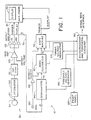
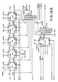
- Fig. l shows a block diagram of a trigger l0 in association with input signal circuitry 20 and a real-time oscilloscope main frame 30.
- the mainframe 30 includes a visual display 40.
- the associated circuitry is for illustration only.
- the trigger is not limited in use to a signal acquisition instrument having an integral display, such as an oscilloscope, but may be used in other instruments as well.
- the input signals to be examined are picked up by probes 50 on input circuitry 20. From the probes, the signals travel along an analog signal path 60 to a visual display 40. These signals may be digital or analog in nature; what is displayed is the analog characteristics of each signal.
- a signal path 70 branches from the analog signal path to direct the analog signals also through the trigger l0. If the logic levels of the analog signals match trigger conditions set by the selected triggering mode, the trigger produces a trigger signal that triggers the display of the corresponding analog signals.
- analog input signal circuitry 20 is of conventional design and present in a separate unit connected to oscilloscope mainframe 30. For clarity, only the circuit elements of one of eight independently controllable input signal channels is depicted, with the eight channels represented by the appropriate notation on line 70.
- Each input signal detected by probe 50 passes through an attenuator l00 that proportionally attenuates the strength of the input signal. From there, each input signal travels through an impedance converter ll0 to maximize signal transfer and a gain amplifier l20 which converts each input signal to a differential signal pair.
- the analog path branches beyond the gain amplifier l20 through three output amplifiers l30, l3l, and l32 that buffer each input signal to provide separate, isolated outputs.
- One branch through output amplifier l30 provides a display signal to mainframe 30, a second branch through output amplifier l3l forms a separate trigger signal, and a third branch through the output amplifier l32 directs each analog signal along line 70 to trigger l0.
- each input signal (a differential pair) encounters logic level discrimination means comprising a comparator circuit l40 and an input portion of a word recognizer 80.
- the comparators l40 compare the input signal against first and second predetermined threshold voltages. The first voltage corresponds to a high logic level, and the second level is lower than the first, corresponding to a low logic level.
- the output of each comparator forms two differential pairs of digital signals that encode the input signal's logic level relative to the threshold voltages.
- the threshold voltages levels are adjustable, set by a threshold voltage generating means l50 such as a digital-to-analog converter under the control of a microprocessor l60.
- Threshold voltages may be selected that correspond to high and low logic levels of different logic families, such as TTL, ECL, or CMOS or may be independently entered by command. Each differential pair is sent along a connecting path 75 to the word recognizer 80. There they are each initially decoded into three separate digital signals that describe the logic level of the input signal above (H), below (L), and transitionally between (T) the predetermined first and second threshold voltage levels.
- the word recognizer 80 receives the digital signals and detects whether a triggering event such as a predetermined combination of input signal logic levels is present.
- the triggering event depends on the triggering mode selected (described herein), which typically includes a predetermined combination of input signals on the input lines.
- the predetermined combination or combinations is set within word recognizer 80 by microprocessor l60.
- An example of such a combination on eight input channels might be: where H represents a logic level above the predetermined high voltage threshold, L represents a logic level below the predetermined low voltage threshold, and T represents a transition logic level between the high and low voltage threshold levels.
- An "X" indicates that a channel is excluded from determination of the combination (a "don't care”).
- a "/" indicates that the channel is selected as a clock and that the recognizer 80 evaluates each input combination on the rising clock edge of that channel. The recognizer can also evaluate the combination on a falling clock edge. If recognizer 80 recognizes the input combination, it generates a recognition signal that is transmitted to the state machine 90. If the triggering event is several predetermined combinations, a plurality of recognition signals are generated.
- Generation of the recognition signals may be qualified by a qualifier (Q) signal l80 that originates at a logic analyzer or similar device monitoring events in the digital system being analyzed.
- Q which is generated by a separate event in that system, is used to restrict the occasions on which a trigger event is detected.
- To sharpen the signal characteristics of Q it is passed through a Schmitt trigger l90 before reaching recognizer 80.
- Recognizer 80 and state machine 90 may be set by command to be either level or edge sensitive to Q.
- the recognition signals are sent from the word recognizer 80 to state machine 90 along a connecting path 78.
- the state machine 90 and the word recognizer 80 form a triggering event detection means in the circuit l0.
- the state machine 90 detects a predetermined sequence of recognition signals within predetermined time windows and measures the duration of the recognition signals.
- the trigger conditions within the state machine are set by the selected triggering mode through the microprocessor l60 and qualified by Q l80.
- the state machine also receives analog voltage input from a timing voltage generator 2l0 that calibrates the frequency of timing apparatus within the machine. Generator 2l0 generates its voltage signal in response to digital input from microprocessor l60.
- the recognition signals are routed through the state machine without further processing to the trigger output.
- the trigger mode is time-based, the signals are evaluated within the state machine for the duration and sequence called for by the triggering mode.
- the mode may specify that the predetermined combination above must exist for a predetermined time:
- state machine 90 If the trigger conditions are satisfied, state machine 90 generates a trigger signal to mainframe 30.
- the trigger signal itself may be displayed along with the analog input signals and other information captured by the triggering mode.
- Choice of triggering mode is made at a control means such as a front panel 230 that communicates with the trigger circuitry through microprocessor l60.
- the modes include four clock-based: single, nested, consecutive, and exception; and eight time-based: single, nested, consecutive, exception, and setup, hold, sliver, and transition. The operation of each is described in detail below.
- the design of the trigger l0 is best understood by reference to Figs. l through l9 and the following description of each circuit component.
- microprocessor and its peripheral circuitry are of conventional design.
- an 80C88 microprocessor and its family of memory and buffer circuits is used. Signals from microprocessor l60 are sent to recognizer 80, state machine 90, and the other circuit portions of trigger l0 through conventional data buses, buffers, and control logic (not separately shown) associated with the microprocessor.
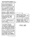
- microprocessor l60 The operation of microprocessor l60 is illustrated by flowcharts in Figs. 20 and 25. The order of steps within each flowchart is for illustration only. The exact order may be varied without affecting the trigger's operation. The flowcharts are discussed in conjunction with the operation of the triggering modes.
- the threshold voltage generator comprises a digital-to-analog converter (DAC) controlled by and receiving digital signals from the microprocessor l60.
- the DAC generates corresponding first (high) and second (low) analog threshold voltage signals, the second being lower than the first, for eight input channels.
- Generator l50 may be implemented by a number of means, the DAC here being a means for illustration only.
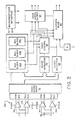
- the microprocessor-originated signal is a binary number that represents the predetermined analog high and low threshold voltages, VTH and VTL, to be sent to comparator circuit l40. Independent high and low threshold voltages are provided for each input differential signal pair, as shown in Fig. 2.
- comparator circuit l40 corresponding to one differential input signal pair 78 is shown in detail in Fig. 2.
- the signal pair is routed to a pair of comparators l4l and l42.
- comparator l4l the signal pair 78 is compared with VTH8, and at comparator l42 the pair is compared with VTL8.
- Each comparator reconstructs the input signal pair 78 into digital differential signal pairs that indicate whether the analog input signals exceed the corresponding threshold voltage level input. If the voltage of the input signal pair 78 exceeds both VTH8 and VTL8, signals VH8+ on comparator l4l and VL8+ on comparator l42 are high and signals VH8- on comparator l4l and VL8- on comparator l42 are low.
- VH8+ is low and VH8- is high on comparator l4l, but VL8+ remains high and VL8- remains low on comparator l42.
- the two differential pairs of signals VH8+, VH8- and VL8+, VL8- thus digitally encode the relative voltage logic level of the input signal pair 78.
- the comparator circuitry makes up one part of the logic level discrimination means of trigger l0.
- the other part comprises the high speed input 8l which is the input portion to word recognizer 80.
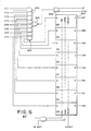
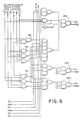
- FIG. 2 A block diagram of word recognizer 80 appears in Fig. 2. The function and operation of each block is discussed below.
- the high speed input which appears at the left of the block diagram of Fig. 2, is shown in context in Fig. 3 and in detail in Fig. 4.
- the two differential pairs of signals VH8+, VH8- and VL8+, VL8- enter a pair of buffers 8ll, 8l2 and are routed therefrom to a decoder 8l5.
- Decoder 8l5 decodes the comparator signals into three separate outputs VH, VT, and VL that correspond to the possible logic levels of the input signal pair 78.
- the decoder 8l5 is of conventional design, constructed of NOR gates 8l5A through 8l5C.
- VTH8 for example, VH is high. If the input signal voltage is between VTH8 and VTL8, VT is high. Only one of the logic level lines VH, VT, VL can be high for each input signal voltage.
- VH, VT, and VL signals are routed to recognizer blocks 83A, 83B, 83C.
- VT is routed alone to a state transition block 84.
- VH and VL are routed to a clock selection block 85 for further processing.
- Recognizer block 83A is shown in detail in Fig. 3, with the circuit diagram of an individual latched multiplexer 830 within the recognizer block shown in Fig. 5.
- Recognizer blocks 83B and 83C are of similar design.
- Recognizer block 83A comprises eight latched multiplexers 830 that include latches 83l, 832 and a multiplexer 833. Referring to Fig. 5, the latches 83l, 832 receive signal select data from microprocessor l60 on lines D0 and Dl to select which of VH, VT, VL or the don't care (X) signals is to be multiplexed. The data is stored in the latches when enabled by lines EN, ENB.
- Multiplexer 830 enables the selected signal VH, VT, VL, or X, and transmits its inverted output on line ZB. If the selected signal is present, ZB is low.
- Fig. 3 shows in circuit context high speed input 8l and recognizer blocks 83A, 83B, 83C.
- the signal select data for multiplexers 830 are carried along the lines IN0 through IN7 from the microprocessor, originating at the far right of the figure and passing through each recognizer block to the left.
- VH, VL, and VT originate at the outputs of high speed inputs 8l and are passed through each recognizer, from left to right across the figure.
- Acceptance by a recognizer of the data signals is controlled by the enabling lines EN, ENB, which are tied to write lines 83W of the microprocessor, shown at the top and bottom of Fig. 3. With this arrangement, each recognizer can be individually configured to recognize a different predetermined combination of input signal levels.
- a recognizer block When a predetermined combination is detected by a recognizer block, it generates recognition signals.
- the recognition signals are formed by ANDing ZB from each multiplexer 833 in the block with the qualifying signal QB and then NORing them together in selectors 835, 836, or 837.
- the output is generated on recognition lines RA, RAB ... RC, RCB.
- the recognition lines connect to a mode control circuit 86, at which the recognition signals required for a specific triggering mode are selected.
- State transition circuit 84 detects the transition logic levels of one or more input signals VT of a predetermined combination.
- the circuit comprises a register of latches 842 and a selector circuit 843.
- Latches 842 receive data signals from microprocessor l60 on input lines IN0 through IN7 to select the input channels desired and also receives control signals on lines EN, ENB to control the operation of the latches.
- the outputs of latches 842 enable or disable AND gates 844 within selector 843 so that the signal on selected VT lines can be passed through. If any of the selected VT lines is high, the output of NOR gate 845 is low. The ST output on the following NOR gate 846 is then low, and STB is high when a transition level is detected.
- the output of the state transition circuit, ST and STB, is sent to mode control 86 which selects it in several of the time-based triggering modes.
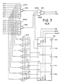
- the clock selection circuit selects an input line as the clock for a predetermined combination, and a rising or falling edge for the clock.
- a register of latches 85l receives selection data signals from microprocessor l60 on input lines IN0 through IN4 and control signals on lines EN, ENB.
- the selection data are gated through the latches to a decoder 852, which decodes the data and enables a single pair of lines VH, VL entering data selectors 853, 854.
- the inverted outputs of these selected lines are then directed to a second stage selector 855, at which the rising (VH) or falling (VL) edge of the clock is chosen.
- a rising clock on channel 7 is detected by disabling all AND gates except 853G and 855B. If the positive edge occurs, the output of selector 853 goes low into selector 855. AND gate 855B is enabled, causing line CK to go high and CKB to go low, indicating the presence of the clocking input. If the falling clock edge was chosen, AND gate 854G and AND gate 855A would instead be enabled.
- the outputs of clock circuit 85 are routed to mode control 86 and high speed output 87.
- Mode control 86 acts as a multiplexer that selects the trigger inputs required for a selected trigger mode.
- These trigger inputs include lines CK from clock circuit 85; ST, STB from state transition circuit 84; and the recognition signals from recognizers 83A, 83B, 83C.
- Data lines M0 through M2B from latches provide the data signals from microprocessor l60 to select the combinations of trigger inputs corresponding to a selected triggering mode. These data signals are decoded in a series of NOR gates 86l and selector circuits 862, 863, and 864. With the appropriate gates enabled, different combinations of the trigger inputs can be selected, corresponding to the chosen trigger mode.
- the outputs R0, R0B ... R2B of the selectors are transmitted to the high speed output 87.
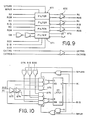
- High speed output 87 is shown in Fig. 9 and, in more detail, in Fig. l0.
- the high speed output receives the outputs R0, R0B ... R2B from the mode control, passes them through filters 87l, and routes them through amplifying drivers 872 to state machine 90.
- Filters 87l are present to filter out false signals that may have been generated internally within the system of circuits, amplifiers, and other components of the trigger l0.
- the output 87 also transmits and amplifies the CKTRG, CKTRGB signals from the clocked mode circuit 89 to the state machine 90, as described below.
- a filter for lines Rl, RlB is shown in detail.
- Rl, RlB are gated through two drivers 873, 874 in series to introduce two delays into the signal's progress.
- the three signals--the original and each delayed signal--then enter AND-NOR gate combinations 875 for Rl and 876 for RlB.
- the other input to each AND gate is controlled by a select line from the microprocessor. With an AND gate enabled by a select line, its output is NORed at NOR gates 875D, 876D with any other output enabled in that group and the inverted output of the respective NOR gate is sent to an SR latch 877.
- Rl is of a predetermined duration
- the SR latch will set, causing the Rl output to be high. If it is not long enough, latch 877 will reset, causing the output Rl to be low.
- the duration can be controlled by enabling different combinations of select lines.
- Rl is less than 300 picoseconds in duration, it is considered internally generated and should be filtered out. If each driver 873, 874 introduces a delay of l50 picoseconds, then Rl will have to be at least 300 picoseconds in duration for all three inputs to AND gates 876 to be low at the same time. If they are, NOR gate 876 sets latch 877. If Rl is less than 300 picoseconds in duration, the previous setting is maintained.
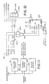
- the clocked mode comprises three circuits: a qualifier circuit 89l, a clock trigger circuit 892, and a status circuit 893.
- qualifier signal Q l80 may be evaluated either on its edge or at a level. This is accomplished within qualifier circuit 89l, shown in detail in Fig. l2.
- Q is selected by microprocessor l60 at gates 89lA and directed to multiplexer 89lB. For level triggering, high or low Q may be selected by enabling lines CNTQEN or CNTQBEN, respectively.
- Q is enabled through edge-triggered latch 89lC.
- PEDGEN and PEDGENB pass Q through gates 89lD as a clock QCK, QCKB to latch 89lC.
- QCK, QCKB will clock a high signal onto output QLQ as Q rises or falls, depending on whether the positive or negative edge was selected via PEDGEN, PEDGENB.
- LATQEN multiplexes QLQ through multiplexer 89lB. The output of the multiplexer is then inverted as QB.
- 89lC is a latch, it must be reset after each output of QLQ. Reset is accomplished by strobe lines QRES and QRESB, which are controlled by CKTRG from clock trigger circuit 892.
- the clock trigger circuit is the trigger for clock-based triggering modes. Referring to Fig. l3, its inputs include the clock input from clock circuit 84, the recognition signals from recognizers 83A through C, and QB from qualifier circuit 89l.
- the microprocessor controls the circuit's operation through lines EN0, ENl.
- the circuit has three latches: trigger latch 892A, reset latch 892B, and arm latch 892C.
- the arm latch detects an initial combination that is an arming event.
- the reset latch detects a following combination that is a reset event, and the trigger latch detects a following combination that is a trigger event.
- the clock input to each latch is CK, CKB from clock circuit 85.
- the data inputs to trigger latch 892A are output signals from recognizers qualified by QB and enabled by microprocessor control lines EN0, ENl.
- the trigger latch's output is CKTRG and CKTRGB, the trigger signal.
- the data inputs to reset latch 892B are also outputs from the recognizers and Q.
- CKRES resets Q, which disables the data inputs to trigger latch 89lA.
- the data inputs to arm latch 892C are an output from recognizers qualified by Q. Its output is used to enable the reset latch and the trigger latch in several triggering modes.
- Circuit 892 also generates signals that affect the operation of qualifier circuit 89l and status circuit 893.
- CKTRG from the trigger latch 892A and CKRES from the reset latch 892B are fed back to circuit 89l to reset edge triggered latch 89lC.
- ARESB is sent to status circuit 893 (Fig. l4) for relay to front panel 230 to show that an arming event or triggering event has been detected.
- the status circuit detects triggering or arming events to provide a status message which assists the user in operation of the instruments.
- the detected signal enters circuit 893 on lines CKTRG or ARESB from the trigger circuit 892 and is stored there by latches 893A through D.
- microprocessor l60 polls the status circuit on line STARD to determine whether a triggering or arming event has occurred. That information is relayed to front panel 230 through the microprocessor l60 and the status circuit 893 is reset.
- the circuit may also be set for self test by microprocessor control on lines MPUR, MPURB.
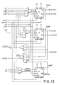
- State machine 90 appears in block diagram in Fig. l5. It receives the trigger inputs R0, Rl, R2 and CKTRG, CKTRGB from recognizer 80. If the trigger conditions of the selected mode are met, it generates trigger signal OTRG to mainframe 30.
- the state machine comprises a number of timer circuits, multiplexers, and selector circuits which are operable in the time-qualified triggering modes. The circuit portions of the state machine are each discussed in detail below.
- output signals from high speed output 87 and CKTRG enter state machine 80 through input receivers 9lA through 9lD.
- the inputs are then passed to following timing multiplexers 92A through 92C for the trigger inputs R0, Rl, R2 and to trigger multiplexer 93 for CKTRGB from clocked mode 89.
- Timing multiplexers 92A through 92C receive the output signals from multiplexers 9lA through 9lC, respectively, and multiplex them to timers 94A through 94C. In this circuit, only timer 94A is truly multiplexed, with 94B and 94C installed solely to match the signal delay through 94A. The other signal inputs to timer 94A originate at trigger circuit 95 and are used in several of the time-based triggering modes.
- Trigger multiplexer 93 appears at the right of Fig. l5. It is controlled by microprocessor l60 to select which of its inputs will be the trigger display signal, OTRG. Its inputs include CKTRGB, which is routed through state machine 80 directly to the trigger, multiplexer terminal counts TC2, TCl, TC0 of timers 94A through 94C, and the TRGTB line from triggering circuit 95. The terminal counts are enabled here only for test purposes, being normally used in conjunction with triggering circuit 95. TRGTB is the triggering signal for time-based triggering modes.
- Timers 94A through 94C are enabled by the presence of input signals that originate at timing multiplexer 92A through C. These signals are the trigger inputs or, in the case of timer 94A, inputs from triggering circuit 95. If the signals are present for a predetermined time, an output signal TC is generated by the timer.
- Fig. l6 The design of the timers is best seen in Fig. l6.
- Input signals from timing multiplexer 92A are routed to a voltage control oscillator (VCO) 94Al and to delay circuitry 94A2.
- VCO voltage control oscillator
- the presence of the signals activates VCO 94Al to provide a clock signal to ripple counter 94A3 through multiplexer 94A4.
- Data inputs to the ripple counter from microprocessor l60 store a predetermined binary number representing a chosen time.
- the QB outputs of each counter eventually go low. When all QB outputs are low, they generate low signals in selector 94A6, which cause a high signal on line TC2.
- Selector 94A6 also has a master reset signal MRES as an input to disable the selector in certain trigger modes.
- Input signals are routed to the delay circuitry 94A2 at the bottom of Fig. l6 to perform two functions. They generate a load signal LD2 that has the inverse value of the trigger input signals that enable the counter 94A3, such that LD2 is high when the trigger inputs are absent and LD is low when the inputs are present. They also actuate the load strobe inputs of ripple counter 94A3 to reload the initial value present on data lines into the counter. For example, if the counter is set for 73 nanoseconds and times to 5 nanoseconds before the enabling trigger input signals disappear, LD will go high and the strobe inputs will reload 73. Latches 94A7, 94A8 and selector circuitry 94A9 are included in delay circuitry 94A2 to match the delay of multiplexers 94A4 and 94A5 in the ripple counter.
- VCO 94Al is calibrated by feedback to microprocessor l60 through outputs Q7 and Q7B at the low end of ripple counter 94A3. Referring back to Fig. l5, Q7 is routed to the microprocessor through data selector circuit 98.
- the qualifier circuit in state machine 80 is identical to that in word recognizer 80.
- the qualifying output QB is routed to triggering circuit 95, as shown in Fig. l5, to qualify the time-qualified modes.
- the trigger signal of trigger multiplexer 93 is routed back to the qualifying circuit to reset Q after a trigger signal has occured.
- Other reset inputs from trigger circuit 95 (lines omitted) also reset Q after a reset event occurs.
- Triggering circuit 95 generates the trigger signal TRGTB for triggering in the time-based modes.
- the circuit 95 comprises three subblocks 95l through 953 that together control the trigger modes.
- Fig. l7 shows output circuitry 95l.
- Fig. l8 shows delay path generator 952.
- Fig. l9 shows multimode sequencer 953.
- the output circuitry generates TRGTB in response to inputs from timers 94A through C, a qualifying signal Q and control signals from microprocessor l60. Those control signals determine what inputs will cause a trigger to occur and what inputs will cause a reset, if any, to result.
- the circuit is constructed around a trigger latch 95lA and a reset latch 95lB. Both are one-shot, such that after each clocks an output, the latch is reset to remove its output signal.
- the data inputs to the trigger latch 95lA are selected through a selector 95lC and the clock is selected through a selector 95lD, both under microprocessor control.
- the trigger signal TRGT that is generated is directed through selector 95lE to generate a qualifier reset QRES and through selector 95lF to generate a timer disable MRES.
- Reset latch 95lB is similar in configuration to trigger latch 95lA.
- Selector 95lG selects data inputs to the latch and selector 95lH selects a clock input, both under microprocessor control.
- the reset output signal is routed back to the data inputs of trigger latch 95lA, to disable the latch if the reset occurs first.
- the delay path generator is designed to mimic the delay of timers 94A through 94C. Referring to Fig. l8, it comprises latches 952A, flip-flop 952B, latch 952C, multiplexers 952D, E, and gates 952F and G. Microprocessor l60 controls the operation of these components as required by the selected mode.
- the EVA7B output of the delay path generator 952 is sent to output circuitry 95l as a clock for the trigger and reset latches.
- the multimode sequencer is used in triggering modes that require prearming and arming events, such as the consecutive and exception modes to be discussed. It comprises a prearm flip-flop 953A and an arm flip-flop 953B that have load inputs and a load strobe as well as data inputs and a clock input. By microprocessor control of the load strobes and the load inputs, prearm and arm signals can be generated in response to input signals.
- a selector 953C is connected to the arm signal output to detect an arming event and relay it to status circuit 97.
- the status circuit within the state machine is indentical to that shown and described in word recognizer 80. It monitors the trigger event in trigger multiplexer 93 and detects the arm event in multimode sequencer 953. Its outputs ARM0Q and TR0Q are routed to front panel 230 on polling by microprocessor l60 to show that the event has occurred.
- Mode operation comprises microprocessor-based commands for setting up the mode and the resulting circuit response to the analog input signals.
- FIG. 20 A flowchart of microprocessor operation in the clock-based modes is shown in Fig. 20.
- the operator initially selects at front panel 230 the triggering mode, the threshold logic levels, the predetermined combination or combinations and the status of the qualifier signal Q.
- the microprocessor in response sends data and control signals to the different circuits within trigger l0. It causes threshold voltage generator l50 to generate the predetermined threshold voltages for comparison with the analog input voltages and loads recognition blocks 83A through 83C with predetermined combinations.
- Clock circuit 84 is also configured to select the predetermined clock channel and rising or falling edge.
- the microprocessor selects the appropriate combination of recognition signals and routes them to clocked mode 89 along with the clock signal from clock circuit 84.
- microprocessor l60 selects the type of qualifying signal desired and the inputs to trigger latch 892A.
- the microprocessor also periodically polls status circuit 893 for arm or trigger events.
- State machine 80 acts as conduit for the trigger signal in the clock-based triggering modes. It is disabled except for trigger multiplexer 93, which selects CKTRG for the trigger display signal that is transmitted to the display 40.
- recognizer block 83A is configured to detect a predetermined combination as the trigger event. For example:
- the recognition signal appears at R2 as a data input to trigger latch 892A.
- the clock input from clock circuit 85 appears as the clock to the trigger latch.
- the trigger latch When the recognition signal is present on a positive clock edge on CK, the trigger latch generates clock trigger signal CKTRG.
- CKTRG is routed to state machine 80 as the trigger display signal OTRG through trigger multiplexer 93.
- Trigger l0 is at an idle state until trigger latch 892A generates CKTRG.
- the trigger signal occurs and initiates a reset of the trigger.
- each event is a predetermined combination evaluated on a clock edge derived from one of the input channels.
- Another predetermined combination forms a reset event.
- the block 83A detects the arming event and generates a recognition signal which is routed through mode control 86 to R0, R0B of clock mode 89.
- R0 is the data input to arm latch 892C, as shown in Fig. l3.
- the qualifier Q is the other input of the arm latch. With the clock signal appearing simultaneously on the clock input to the latch, latch 892C generates an arm signal. This arm signal is directed to the data inputs of trigger latch 892A and the data inputs of reset latch 892B.
- trigger latch 892A With the arm signal present, the data inputs of trigger latch 892A goes high when a trigger event (5) appears contemporaneously on R2 from block 83C. With both present, a clock pulse on channel two will generate a trigger signal from the trigger latch.
- the nested mode also specifies a predetermined combination (6) for resetting the mode if that event appears before the triggering event.
- a predetermined combination (6) for resetting the mode if that event appears before the triggering event.
- the reset occurs if combination (6) is detected on recognizer 83B and routed on Rl to the reset latch. If a clock pulse on channel two is present contemporaneously with Rl and the arming signal, latch 892B generates a reset signal CKRES. This signal also disables trigger latch 892A.
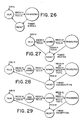
- the operation of this mode is shown in the state diagram of Fig. 22.
- the trigger is in the idle state with the qualifier signal low. When the arming event appears, the trigger is armed. It may then trigger if the trigger event is detected or it may reset if the reset event is detected. After a trigger signal is generated, the trigger is reset.
- the trigger occurs after a predetermined arming event combination is detected and is followed immediately by one of two predetermined combinations that form a triggering event. Any other combination following the arming event is a reset event. For example:
- mode control 86 selects recognizer block 83C to detect the arming event and route its recognition signal to R0 and Rl.
- Blocks 83A and 83B each detect one of the two combinations that are the triggering event and route their recognition signals to R2.
- R0 then provides the input to arm latch 892C along with the qualifier signal Q.
- the arm signal occurs and is routed to reset latch 892B and trigger latch 892A. If a triggering event appears on R2 contemporaneously with a following clock input on channel six, a trigger signal occurs. On the other hand, if an armed false event occurs on Rl contemporaneously with a clock input on channel six, the reset latch generates a reset signal, which disables trigger latch 892A.
- Trigger l0 is in the idle state until the arming event (7) is detected on recognizer C. With the trigger armed, it can either trigger or reset depending on which event next follows. After either occurs, the trigger is reset.
- This mode is similar in operation to the consecutive mode with the input to R2 inverted.
- the trigger occurs in this mode if, after the occurrence of a first combination forming an arming event, two predetermined combinations forming a reset event are absent immediately after the first combination disappears. If either of those two predetermined combinations is present, a reset occurs. Otherwise, any other combination forms a trigger event.
- the arming combination l0 is routed to R ⁇ and combinations (ll, l2) are ORed and routed to Rl.
- a combination other than (ll, l2) is routed to R2.
- reset latch 892B If one of the two second predetermined combinations appears contemporaneously with the clock input on channel seven, reset latch 892B generates a reset signal.
- trigger latch 892A generates a clock trigger signal.
- the state diagram of Fig. 24 shows the sequence of operation of this mode.
- FIG. 25 A flowchart of microprocessor operation in the time-based modes is shown in Fig. 25.
- the operator initially selects at front panel 230 the trigger mode, the threshold logic levels, the predetermined combination or combinations, and the status of the qualifier signal Q. In addition, the operator selects the durations for the predetermined combinations.
- the microprocessor sends data and control signals to the different circuits within trigger l0. It causes threshold voltage generator l50 to generate the predetermined threshold voltages for comparison with the analog input voltages. It commands high speed input 8l to select the real signal inputs and loads register blocks 83A through 83C with the predetermined combinations. It also configures state transition circuit 83 and clock circuit 84.
- the microprocessor selects for a selected triggering mode the appropriate combination of recognition signals, state transition signals, and clock signals and routes them to high speed output 87. It also sends the appropriate signals to timers 94A through 94C for the predetermined durations and controls the operation of the data selectors and multiplexers within state machine 80.
- each time-based trigger mode is shown by state diagrams in Figs. 26 through 33.
- TRTGB from trigger circuit 95 is the trigger display signal.
- the trigger detects the occurrence of a predetermined combination for a predetermined time as the triggering event. For example:
- Recognizer block 83A detects the predetermined combination (l3) and sends its recognition signal through mode 86 to inputs R2, R2B at input receiver 9lA, shown in Figs. l5, l6.
- the microprocessor selects these inputs in timing multiplexer 92A to enable timer 94A.
- the timer previously loaded by microprocessor l60 with a predetermined time represented by a binary number, starts counting when the inputs are present on the enable lines. If the counter counts out, line TC2 goes high. Referring to Fig. l7, TC2 is the clock input on selector 95lD to the trigger latch 95lA.
- the data input to latch 95lA is selected by selector 95lC to be QB, with all other lines disabled.
- TRTGB is routed to trigger multiplexer 93 and TRGT, its complement, resets trigger latch 95lA and reset latch 95lB.
- timer 94A If the recognition signals disappear at the enable inputs to timer 94A, the timer is reloaded automatically.
- timer 94A waits continuously in its idle state until a recognition signal of sufficient duration is detected.
- the trigger occurs in the second of two events, where event is a predetermined combination having a predetermined duration.
- a combination representing a reset event may also be specified.
- Each of the recognizer blocks is used.
- Timer 94B is the arm timer and receives inputs from recognizer block 83B through Rl.
- Timer 94A is a reset timer and receives its inputs from recognizer block 83C through R2.
- Timer 94C is a trigger timer and receives its inputs from recognizer block 83A through R0.
- TC0 forms a clock input to trigger latch 95lA through selector 95lD.
- the data inputs to the trigger latch are an enable signal from the microprocessor and the qualifier signal QB. With the qualifier present, the trigger latch will generate a trigger signal on the appearance of TC0.
- TC2 goes high.
- TC2 in this mode is the clock for reset latch 95lB.
- the data input to the reset latch is set high by microprocessor control.
- the reset signal generated by latch 95lB causes MRES to go high to reset latch 953B, as shown in Fig. l9.
- the reset signal is also routed to trigger latch 95lA to disable the data input, thereby preventing a trigger signal from occurring after a reset signal.
- a trigger occurs after a first predetermined combination selected as an arming event is detected and followed within a window of time by one of two predetermined combinations forming a trigger event. If those combinations do not occur within that window, the trigger is reset. For example:
- timer 94C is the prearm timer; timer 94B is the arm timer; and timer 94A is the time window timer.
- recognizer block 83C detects combination (l7) and routes its recognition signal to R0, R0B of timer 94C. If it is present for the predetermined time, the timer successfully times out and TC0 goes high. Referring to Fig. l9, TC0 then clocks a high signal on latch 953A. The trigger is now prearmed.
- the second step in this mode is the disappearance of the first combination for a predetermined time. This is measured on arm timer 94B.
- timer Rl, RlB
- the inputs to that timer, Rl, RlB are the complement of the inputs to R0, R0B.
- Rl goes high and timer 94B begins to time. If it successfully times out, TCl goes high, clocking through latch 953B the high signal from latch 953A to generate ARM, ARMB.
- ARM, ARMB are fed back to the inputs of timing multiplexer 92A and selected by microprocessor control to be the enabling inputs to timer 94A. They start the time window. While it is active, inputs R2, R2B are routed to inputs EN2, EN2B of trigger circuit 95, which appear in the delay path generator of Fig. l8.
- the microprocessor enables multiplexer 952D to accept these input signals and route them through multiplexer 952E to the output gate 952F.
- the output that results is EVA7B, which is the complement of the enable inputs. Thus, if combinations (l8, l9) are present during the time window, EVA7B is low.
- EVA7B is NORed with LD2 to form EVA8 as a clock input to trigger latch 95lA.
- LD2 is low and EVA8 high to clock the trigger latch.
- TC2 which forms the data input to the trigger latch, is low if the window is present. Thus, the data input to the trigger latch is high, and a trigger signal is generated by trigger latch 95lA.
- TC2 will be high and the data input to the trigger latch will be low so that no trigger signal can be generated. TC2 will also clock a high value into reset latch 95lD, causing a reset signal to be generated that resets latches 953A, 953B and disables the trigger latch 95lA.
- a state diagram of the triggering mode is shown. From the idle stage, the trigger moves to a prearm stage, an arm stage, and then either triggers or resets, depending upon the combinations that occur.
- a trigger occurs after a first predetermined combination forming an arming event is detected followed within a window of time by the absence of two predetermined combinations. Otherwise, the trigger resets if either combination occurs. For example:
- EVA8 (Fig. l7) is used as a clock input to reset latch 95lB rather than a clock input to trigger latch 95lA. This is accomplished by microprocessor control.
- TC2 of timer 94A becomes the data input to the reset latch through selector 95lG and the clock input to trigger latch 95lA through selector 95lC.
- the data input to the trigger latch is the qualifier signal QB.
- TC2 will cause trigger latch 95lA to generate a trigger signal. If the predetermined combinations are present, EVA8 will cause reset latch 95lB to generate a reset signal, which will then disable the trigger latch, as before. Referring to Fig. 29, a state diagram of this triggering mode is shown.
- the setup-time violation detects as the trigger event a transition logic level on one or more input lines present within a predetermined time prior to a clock signal.
- input signals can be checked to see if they are stable for a sufficient time before a clock edge. For example:
- signal STB from state transition circuit 83 is routed through mode control 86 to input R2 of timer 94A.
- the clock signal from clock circuit 84 is routed through mode control 86 to inputs R0, R0B and from there to inputs EN0, EN0B of triggering circuit 95.
- timer 94A With STB present, timer 94A will count down the predetermined time, indicating that the state transition is absent for the predetermined time. If it times out, TC2 goes high. Referring to Fig. l7, TC2 forms a data input to trigger latch 95lC. If TC2 is high, then the data input to the trigger latch is low and no trigger signal is generated. If the timer has not timed out, TC2 will be low and a trigger signal will be generated.
- the clock input to the trigger latch is produced through the delay path generator of Fig. l8.
- EN0, EN0B clock a high signal through latch 952B.
- This signal propagates the multiplexer 952E and latch 952C to produce a low output on EVA7B.
- EVA7B is NORed with LD2, which is low if STB is present on the enable lines of timer 94A.
- the NOR gate output, EVA8, will then be high to generate a clock pulse to trigger latch 95lA.
- This mode also has a qualifier combination (24) on the input lines not used for transition logic levels. These lines produce a recognition signal on recognizer block 83C which is routed to inputs Rl, RlB of timer 94B. The timer is not used in this mode, but the enable lines indicate the combination's presence or absence by a signal on LDl. If the inputs are present, LDl is low. Referring to Fig. l7, LDl qualifies the data input to trigger latch 95lA along with TC2. If the combination is absent, LDl is high, disabling the data input and thereby preventing the generation of a trigger signal.
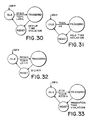
- FIG. 30 A state diagram of the triggering mode is shown in Fig. 30.
- the hold-time violation detects as the trigger event input signals that are in the transition logic level within a predetermined time after a clock edge.
- CK CKB are input lines on R0, R0B and are routed to EN0, EN0B, as shown in Fig. l5 and l8.
- These inputs clock a high output on latch 952B which is routed out of trigger circuit 95 by way of lines EVAl and EVAlB, rather than through multiplexer 952E.
- EVAl and EVAlB are then multiplexed by timing multiplexer 92A as enabling inputs to timer 94A.
- the transition signal input ST enters state machine 80 through R2, R2B and is routed to EN2, EN2B, also shown in Fig. l8.
- these input strobe a low output on latch 952A and route it through multiplexer 952D to produce an output signal EVA7B.
- EVA7B is NORed with LD2 to form clock input EVA8 to trigger latch 95lC.
- TC2 will go high to disable the data input to the trigger latch and no trigger signal will occur when EVA8 clocks the trigger latch. If timer 94A has not timed out, TC2 will be low and latch 95lA will then generate a trigger signal upon a clock pulse.
- the hold time violation mode may also be qualified by a predetermined combination (26) on those lines not selected for monitoring of transition logic levels. This combination is detected by recognizer block 83B and routed to Rl, RlB of timer 94B. If the combination is present, LDl is low. If the combination disappears, LDl goes high, disabling the data input and preventing the trigger latch from generating a trigger signal. Referring to Fig. 3l, a state diagram of the triggering mode is shown.
- a sliver is defined as a pulse which exists for less than a predetermined reference time.
- the sliver detected as a trigger event is an excursion from and return to a predetermined logic level on one input channel within a predetermined time while the other channels are configured as a qualifying event. For example:
- the sliver is detected as a clock pulse on clock circuit 84.
- the clock pulse is routed to R2, R2B to enable timer 94A. If the clock signal returns to its original value, the timer will stop counting. But, so long as the clock signal does not return, the timer counts down.
- the output TC2 forms the data input to trigger latch 95lA.
- the clock input to the trigger latch is line LD2 from timer 94A. This line goes high when the sliver disappears. The trigger then occurs, if at all, after the sliver has disappeared (the clock signal returning to its original level). If timer 94A has timed out at that point, TC2 will be high and will disable the data input to trigger latch 95lA. If TC2 has not timed out at the time the signal disappears, TC2 will be low and a trigger signal will be generated on the occurrence of a high signal on LD2.
- the combination (28) selected as the qualifying event is routed from recognizer 83B to Rl, RlB. It enables LDl, causing LDl to be low so as not to affect the data input to trigger latch 95lA. If the qualifying combination disappears, LDl goes high and disables the data input, thereby preventing the latch from generating a trigger signal.
- Fig. 32 shows the state diagram of this triggering mode.
- the trigger event is a transition detected on one channel and lasting for greater than a predetermined time.
- the other channels may be configured as a qualifying event. For example:
- Transition signal ST from state transition circuit 83 is routed through mode control 86 to R2, R2B to enable timer 94A.
- TC2 from timer 94A forms the clock input for trigger latch 95lA, with the data input provided by the qualifying signal QB. If the trigger event is present for the predetermined time, TC2 goes high to clock the data input into trigger latch 95lA which generates a trigger signal if Q is present. If ST disappears before the timer times out, the timer is automatically reloaded and the mode begins again.
- the combination (30) selected as the qualifying event is detected by recognizer 83B and is routed through mode control 86 to inputs Rl, RlB to enable timer 94B.
- the presence of a qualifying event causes LDl to be low, enabling the data input to trigger latch 95lA. If the qualifying event disappears, LDl goes high to disable the data input and thereby prevent the latch from generating a trigger signal.
- the state diagram of this triggering mode is shown in Fig. 33.
Abstract
Description
- This invention relates to electronic triggering devices, and more particularly to triggering devices for detecting and displaying the analog characteristics of multiple simultaneous signals.
- The design of electronic circuits has become increasingly complex with the advent of microprocessor-based systems. Troubleshooting such circuits demands instruments that can capture simultaneous digital signals and display their analog characteristics. Conventional oscilloscopes that are quick enough to view the subnanosecond pulses of these signals lack the capability to trigger on a combination (referred to as a word) or series of combinations of these signals. Logic analyzers, on the other hand, excel at triggering on words. But they lack an oscilloscope's ability to display the voltage and timing characteristics of the digital signals that form the word.
- Several attempts have been made to address this demand by incorporating the measurement capability of the oscilloscope and the recognition capability of the logic analyzer into a single device. Devices of this type include the 7A42, an oscilloscope logic triggered amplifier manufactured by Tektronix, Inc., of Beaverton, Oregon, and now the subject of U.S. Patent Application Serial No. 06/487,398; the Microanalyst, a timing analyzer manufactured by Northwest Instruments, Inc., of Beaverton, Oregon; and the 54l00D, a digital oscilloscope manufactured by Hewlett-Packard Company of Palo Alto, California. These devices vary from each other primarily in the triggering modes they offer.
- The 7A42 is designed to trigger on a single word or a nested sequence of Boolean words and to display the corresponding analog characteristics of the signals that form each word. In the single word combination of inputs, it can trigger either immediately on the appearance of a predetermined combination or after the combination has persisted for a predetermined time. In the nested mode, it triggers on the appearance of a sequence of a first predetermined combination followed immediately by a second predetermined word combination.
- The Microanalyzer lacks an analog display of the digital signals but offers other triggering modes not found in logic analyzers or the 7A42. In addition to the single word and nested triggering modes, it can trigger on a digital signal that is detected between predetermined logic levels within a predetermined time of a clock pulse.
- The 54l00D offers analog signal display capability and includes several triggering modes not available in the instruments above. Like the logic analyzer and other devices, it can trigger on a single word, both immediately and after the word's persistence for a predetermined time. The 54l00D can also detect and trigger on a narrow pulse, or glitch, and display the pulse's analog characteristics. In addition, it can be set to trigger after the occurrence of a predetermined number of events or a predetermined time. However, it cannot trigger on nested sequence of word combinations without the aid of a logic analyzer.
- These devices are great improvements over what was previously possible with a conventional logic analyzer or oscilloscope. But they lack the capability of triggering in many other circumstances where it is desirable to view the analog characteristics of the signals within a system. For example, none of them can detect and display the analog characteristics of a plurality of digital signals transitionally between high and low logic levels. Nor can they detect a sequence of a first predetermined word combination followed by one of two second predetermined combinations. They also cannot detect a sequence of a first predetermined combination followed by the absence of one of two second predetermined combinations. And none of these devices offers all these triggering modes in a single device that can monitor up to eight input signal channels simultaneously.
- It is an object of the invention to provide a triggering device that offers a plurality of triggering modes for measuring the analog characteristics of input signals.
- A second object of the invention is to provide a triggering device that can detect up to eight simultaneous input signals.
- A third object of the invention is to provide a triggering device that can detect the high, low, and transistion logic levels of input signals.
- Another object of the invention is to provide a triggering device that can detect the transition logic level on an input signal within a predetermined time of a clock pulse.
- Yet another object of the invention is to provide a triggering device that can detect a first predetermined combination of input signal logic levels followed by the presence or absence of a second predetermined combination.
- To achieve these objects, a trigger circuit for detecting plural analog input signals includes logic level discrimination means for reconstructing each input signal into a number of digital signals and trigger event detection means for detecting in the digital signals a triggering event. The logic level discrimination means reconstructs each input signal in response to predetermined first and second threshold levels to describe the input signal's logic level above the first threshold level, below the second threshold level, and transitionally between the first and second levels. The triggering event detected by the detection means includes at least one predetermined combination of input signal logic levels. Upon detection of the triggering event, the trigger circuit generates a trigger display signal.
- In this embodiment of the invention, the predetermined first and second threshold logic levels are voltage levels that are selectably adjustable and are generated by threshold voltage generator means.
- The trigger event detection means can detect triggering events in both clock-based and time-based triggering modes. The clock-based modes include single event triggering, nested triggering, and consecutive and an exception triggering. In the consecutive mode, the detection means detects a sequence of a first predetermined combination of input signal logic levels followed immediately by one of two second predetermined combinations. In the exception mode, the detection means detects sequence of a first predetermined combination of input signal logic levels followed immediately by the absence of a second predetermined combination.
- In the time-based triggering modes, a user-definable time window is provided for detecting predetermined combinations. For the timed-consecutive mode, the detection means detects a first predetermined combination lasting for a predetermined time followed by one of two second predetermined combinations within a predetermined window of time. For the timed-exception mode, the detection means detects a first predetermined combination lasting for a predetermined time followed within a predetermined time window by the absence of a second predetermined combination. Other modes include setup time or hold time violation modes. In these modes, the detection means detects the transition logic level of an input signal occurring within a predetermined time of a clock pulse detected on another input signal. In a sliver detection mode, the detection means detects on an input signal an excursion from and the return to a predetermined logic level, the excursion and return occurring within a predetermined time window. And in a transition time violation mode, the detection means detects a transition logic level on an input signal enduring greater than or less than a predetermined time.
- In this embodiment, the detection means comprises a word recognizer for recognizing predetermined combinations of input signal logic levels and a state machine for time-qualifying the combinations recognized by the recognizer. The detection means may also include a trigger filter for filtering out internally-generated signals of less than a predetermined duration.
- The foregoing and other objects, features, and advantages of the invention will become more apparent from the following detailed description of a preferred embodiment which proceeds with reference to the accompanying drawings.
-
- FIG. l is a block diagram of the preferred embodiment of the present invention.
- FIG. 2 is a schematic diagram of the comparator circuitry and a block diagram of the word recognizer of Fig. l.
- FIG. 3 is a schematic diagram of the high speed input and recognizer blocks of Fig. 2.
- FIG. 4 is a schematic diagram of the high speed input block of the word recognizer.
- FIG. 5 is a schematic diagram of a recognizer multiplexer that forms the recognizer block.
- FIG. 6 is a schematic diagram of the state transition block.
- FIG. 7 is a schematic diagram of the clock circuitry block.
- FIG. 8 is a schematic diagram of the mode control block.
- FIG. 9 is a schematic diagram of the high speed output block.
- FIG. l0 is a schematic diagram of the filter circuitry of the high speed output block.
- FIG. ll is a subblock diagram of the clock mode block.
- FIG. l2 is a schematic diagram of the qualifier subblock of the clock mode block.
- FIG. l3 is a schematic diagram of the clock circuit subblock of the clock mode block.
- FIG. l4 is a schematic diagram of the status circuit subblock of the clock mode block.
- FIG. l5 is a block diagram of the state machine of Fig. l.
- FIG. l6 is a schematic diagram of the timing circuit block of the state machine.
- FIG. l7 is a schematic diagram of a portion of the trigger circuit block.
- FIG. l8 is schematic diagram of a second portion of the trigger circuit block.
- FIG. l9 is a schematic diagram of a third portion of the trigger circuit block.
- FIG. 20 is a flowchart of microprocessor operation in clock-based triggering modes.
- FIG. 2l is a state diagram of the clock-single triggering mode.
- FIG. 22 is a state diagram of the clocked-nested triggering mode.
- FIG. 23 is a state diagram of clocked-consecutive triggering mode.
- FIG. 24 is a state diagram of clocked-exception triggering mode.
- FIG. 25 is a flowchart of microprocessor operation in time-based triggering modes.
- FIG. 26 is a state diagram of the timed-single triggering mode.
- FIG. 27 is a state diagram of the timed-nested triggering mode.
- FIG. 28 is a state diagram of the timed-consecutive triggering mode.
- FIG. 29 is a state diagram of the timed-exception triggering mode.
- FIG. 30 is a state diagram of the setup time violation triggering mode.
- FIG. 3l is a state diagram of the hold-time violation triggering mode.
- FIG. 32 is a state diagram of the sliver detection triggering mode.
- FIG. 33 is a state diagram of the transition time violation triggering mode.
- Fig. l shows a block diagram of a trigger l0 in association with
input signal circuitry 20 and a real-time oscilloscopemain frame 30. Themainframe 30 includes avisual display 40. The associated circuitry is for illustration only. The trigger is not limited in use to a signal acquisition instrument having an integral display, such as an oscilloscope, but may be used in other instruments as well. - The input signals to be examined are picked up by
probes 50 oninput circuitry 20. From the probes, the signals travel along ananalog signal path 60 to avisual display 40. These signals may be digital or analog in nature; what is displayed is the analog characteristics of each signal. Asignal path 70 branches from the analog signal path to direct the analog signals also through the trigger l0. If the logic levels of the analog signals match trigger conditions set by the selected triggering mode, the trigger produces a trigger signal that triggers the display of the corresponding analog signals. - Considering Fig. l in more detail, analog
input signal circuitry 20 is of conventional design and present in a separate unit connected tooscilloscope mainframe 30. For clarity, only the circuit elements of one of eight independently controllable input signal channels is depicted, with the eight channels represented by the appropriate notation online 70. Each input signal detected byprobe 50 passes through an attenuator l00 that proportionally attenuates the strength of the input signal. From there, each input signal travels through an impedance converter ll0 to maximize signal transfer and a gain amplifier l20 which converts each input signal to a differential signal pair. The analog path branches beyond the gain amplifier l20 through three output amplifiers l30, l3l, and l32 that buffer each input signal to provide separate, isolated outputs. One branch through output amplifier l30 provides a display signal tomainframe 30, a second branch through output amplifier l3l forms a separate trigger signal, and a third branch through the output amplifier l32 directs each analog signal alongline 70 to trigger l0. - Upon entering the trigger l0, each input signal (a differential pair) encounters logic level discrimination means comprising a comparator circuit l40 and an input portion of a
word recognizer 80. The comparators l40 compare the input signal against first and second predetermined threshold voltages. The first voltage corresponds to a high logic level, and the second level is lower than the first, corresponding to a low logic level. The output of each comparator forms two differential pairs of digital signals that encode the input signal's logic level relative to the threshold voltages. The threshold voltages levels are adjustable, set by a threshold voltage generating means l50 such as a digital-to-analog converter under the control of a microprocessor l60. Threshold voltages may be selected that correspond to high and low logic levels of different logic families, such as TTL, ECL, or CMOS or may be independently entered by command. Each differential pair is sent along a connectingpath 75 to theword recognizer 80. There they are each initially decoded into three separate digital signals that describe the logic level of the input signal above (H), below (L), and transitionally between (T) the predetermined first and second threshold voltage levels. - The
word recognizer 80 receives the digital signals and detects whether a triggering event such as a predetermined combination of input signal logic levels is present. The triggering event depends on the triggering mode selected (described herein), which typically includes a predetermined combination of input signals on the input lines. The predetermined combination or combinations is set withinword recognizer 80 by microprocessor l60. An example of such a combination on eight input channels might be:
where H represents a logic level above the predetermined high voltage threshold, L represents a logic level below the predetermined low voltage threshold, and T represents a transition logic level between the high and low voltage threshold levels. An "X" indicates that a channel is excluded from determination of the combination (a "don't care"). A "/" indicates that the channel is selected as a clock and that the
recognizer 80 evaluates each input combination on the rising clock edge of that channel. The recognizer can also evaluate the combination on a falling clock edge. Ifrecognizer 80 recognizes the input combination, it generates a recognition signal that is transmitted to thestate machine 90. If the triggering event is several predetermined combinations, a plurality of recognition signals are generated. - Generation of the recognition signals may be qualified by a qualifier (Q) signal l80 that originates at a logic analyzer or similar device monitoring events in the digital system being analyzed. Q, which is generated by a separate event in that system, is used to restrict the occasions on which a trigger event is detected. To sharpen the signal characteristics of Q, it is passed through a Schmitt trigger l90 before reaching
recognizer 80.Recognizer 80 andstate machine 90 may be set by command to be either level or edge sensitive to Q. - The recognition signals are sent from the
word recognizer 80 tostate machine 90 along a connectingpath 78. Thestate machine 90 and theword recognizer 80 form a triggering event detection means in the circuit l0. Thestate machine 90 detects a predetermined sequence of recognition signals within predetermined time windows and measures the duration of the recognition signals. As withrecognizer 80, the trigger conditions within the state machine are set by the selected triggering mode through the microprocessor l60 and qualified by Q l80. The state machine also receives analog voltage input from a timing voltage generator 2l0 that calibrates the frequency of timing apparatus within the machine. Generator 2l0 generates its voltage signal in response to digital input from microprocessor l60. - If the trigger mode selected is clock-based, as in the example (l), the recognition signals are routed through the state machine without further processing to the trigger output. If the trigger mode is time-based, the signals are evaluated within the state machine for the duration and sequence called for by the triggering mode. For example, the mode may specify that the predetermined combination above must exist for a predetermined time:

- If the trigger conditions are satisfied,
state machine 90 generates a trigger signal tomainframe 30. The trigger signal itself may be displayed along with the analog input signals and other information captured by the triggering mode. - Choice of triggering mode is made at a control means such as a
front panel 230 that communicates with the trigger circuitry through microprocessor l60. The modes include four clock-based: single, nested, consecutive, and exception; and eight time-based: single, nested, consecutive, exception, and setup, hold, sliver, and transition. The operation of each is described in detail below. - The design of the trigger l0 is best understood by reference to Figs. l through l9 and the following description of each circuit component.
- The microprocessor and its peripheral circuitry are of conventional design. In this embodiment, an 80C88 microprocessor and its family of memory and buffer circuits is used. Signals from microprocessor l60 are sent to
recognizer 80,state machine 90, and the other circuit portions of trigger l0 through conventional data buses, buffers, and control logic (not separately shown) associated with the microprocessor. - The operation of microprocessor l60 is illustrated by flowcharts in Figs. 20 and 25. The order of steps within each flowchart is for illustration only. The exact order may be varied without affecting the trigger's operation. The flowcharts are discussed in conjunction with the operation of the triggering modes.
- The threshold voltage generator comprises a digital-to-analog converter (DAC) controlled by and receiving digital signals from the microprocessor l60. The DAC generates corresponding first (high) and second (low) analog threshold voltage signals, the second being lower than the first, for eight input channels. Generator l50 may be implemented by a number of means, the DAC here being a means for illustration only. The microprocessor-originated signal is a binary number that represents the predetermined analog high and low threshold voltages, VTH and VTL, to be sent to comparator circuit l40. Independent high and low threshold voltages are provided for each input differential signal pair, as shown in Fig. 2.
- A portion of comparator circuit l40 corresponding to one differential
input signal pair 78 is shown in detail in Fig. 2. The signal pair is routed to a pair of comparators l4l and l42. At comparator l4l thesignal pair 78 is compared with VTH8, and at comparator l42 the pair is compared with VTL8. Each comparator reconstructs theinput signal pair 78 into digital differential signal pairs that indicate whether the analog input signals exceed the corresponding threshold voltage level input. If the voltage of theinput signal pair 78 exceeds both VTH8 and VTL8, signals VH8+ on comparator l4l and VL8+ on comparator l42 are high and signals VH8- on comparator l4l and VL8- on comparator l42 are low. If the input signal voltage exceeds only VTL8, then VH8+ is low and VH8- is high on comparator l4l, but VL8+ remains high and VL8- remains low on comparator l42. The two differential pairs of signals VH8+, VH8- and VL8+, VL8- thus digitally encode the relative voltage logic level of theinput signal pair 78. - The comparator circuitry makes up one part of the logic level discrimination means of trigger l0. The other part comprises the high speed input 8l which is the input portion to
word recognizer 80. - A block diagram of
word recognizer 80 appears in Fig. 2. The function and operation of each block is discussed below. - The high speed input (HSIN), which appears at the left of the block diagram of Fig. 2, is shown in context in Fig. 3 and in detail in Fig. 4. Referring to Fig. 4, the two differential pairs of signals VH8+, VH8- and VL8+, VL8- enter a pair of buffers 8ll, 8l2 and are routed therefrom to a decoder 8l5. Decoder 8l5 decodes the comparator signals into three separate outputs VH, VT, and VL that correspond to the possible logic levels of the
input signal pair 78. The decoder 8l5 is of conventional design, constructed of NOR gates 8l5A through 8l5C. If the input signal voltage is above the high voltage threshold level, VTH8 for example, VH is high. If the input signal voltage is between VTH8 and VTL8, VT is high. Only one of the logic level lines VH, VT, VL can be high for each input signal voltage. - Referring again to Fig. 2, the VH, VT, and VL signals are routed to
recognizer blocks state transition block 84. And VH and VL are routed to aclock selection block 85 for further processing. -
Recognizer block 83A is shown in detail in Fig. 3, with the circuit diagram of an individual latchedmultiplexer 830 within the recognizer block shown in Fig. 5. Recognizer blocks 83B and 83C are of similar design.Recognizer block 83A comprises eight latchedmultiplexers 830 that includelatches 83l, 832 and amultiplexer 833. Referring to Fig. 5, thelatches 83l, 832 receive signal select data from microprocessor l60 on lines D0 and Dl to select which of VH, VT, VL or the don't care (X) signals is to be multiplexed. The data is stored in the latches when enabled by lines EN, ENB. -
Multiplexer 830 enables the selected signal VH, VT, VL, or X, and transmits its inverted output on line ZB. If the selected signal is present, ZB is low. - Fig. 3 shows in circuit context high speed input 8l and
recognizer blocks multiplexers 830 are carried along the lines IN0 through IN7 from the microprocessor, originating at the far right of the figure and passing through each recognizer block to the left. VH, VL, and VT originate at the outputs of high speed inputs 8l and are passed through each recognizer, from left to right across the figure. Acceptance by a recognizer of the data signals is controlled by the enabling lines EN, ENB, which are tied to writelines 83W of the microprocessor, shown at the top and bottom of Fig. 3. With this arrangement, each recognizer can be individually configured to recognize a different predetermined combination of input signal levels. - When a predetermined combination is detected by a recognizer block, it generates recognition signals. The recognition signals are formed by ANDing ZB from each multiplexer 833 in the block with the qualifying signal QB and then NORing them together in
selectors mode control circuit 86, at which the recognition signals required for a specific triggering mode are selected. -
State transition circuit 84 detects the transition logic levels of one or more input signals VT of a predetermined combination. Referring to Fig. 6, the circuit comprises a register oflatches 842 and aselector circuit 843.Latches 842 receive data signals from microprocessor l60 on input lines IN0 through IN7 to select the input channels desired and also receives control signals on lines EN, ENB to control the operation of the latches. The outputs oflatches 842 enable or disable ANDgates 844 withinselector 843 so that the signal on selected VT lines can be passed through. If any of the selected VT lines is high, the output of NORgate 845 is low. The ST output on the following NORgate 846 is then low, and STB is high when a transition level is detected. - The output of the state transition circuit, ST and STB, is sent to
mode control 86 which selects it in several of the time-based triggering modes. - The clock selection circuit, shown in Fig. 7, selects an input line as the clock for a predetermined combination, and a rising or falling edge for the clock. As in
state transition circuit 84, a register of latches 85l receives selection data signals from microprocessor l60 on input lines IN0 through IN4 and control signals on lines EN, ENB. The selection data are gated through the latches to adecoder 852, which decodes the data and enables a single pair of lines VH, VL enteringdata selectors second stage selector 855, at which the rising (VH) or falling (VL) edge of the clock is chosen. For example, a rising clock on channel 7 is detected by disabling all AND gates except 853G and 855B. If the positive edge occurs, the output ofselector 853 goes low intoselector 855. ANDgate 855B is enabled, causing line CK to go high and CKB to go low, indicating the presence of the clocking input. If the falling clock edge was chosen, ANDgate 854G and ANDgate 855A would instead be enabled. - The outputs of
clock circuit 85 are routed tomode control 86 andhigh speed output 87. -
Mode control 86 is shown in Fig. 8. It acts as a multiplexer that selects the trigger inputs required for a selected trigger mode. These trigger inputs include lines CK fromclock circuit 85; ST, STB fromstate transition circuit 84; and the recognition signals from recognizers 83A, 83B, 83C. Data lines M0 through M2B from latches (not shown) provide the data signals from microprocessor l60 to select the combinations of trigger inputs corresponding to a selected triggering mode. These data signals are decoded in a series of NOR gates 86l andselector circuits high speed output 87. -
High speed output 87 is shown in Fig. 9 and, in more detail, in Fig. l0. As shown in Fig. 9, the high speed output receives the outputs R0, R0B ... R2B from the mode control, passes them through filters 87l, and routes them through amplifyingdrivers 872 tostate machine 90. Filters 87l are present to filter out false signals that may have been generated internally within the system of circuits, amplifiers, and other components of the trigger l0. Theoutput 87 also transmits and amplifies the CKTRG, CKTRGB signals from the clockedmode circuit 89 to thestate machine 90, as described below. - Referring to Fig. l0, a filter for lines Rl, RlB is shown in detail. Rl, RlB are gated through two
drivers gate combinations 875 for Rl and 876 for RlB. The other input to each AND gate is controlled by a select line from the microprocessor. With an AND gate enabled by a select line, its output is NORed at NOR gates 875D, 876D with any other output enabled in that group and the inverted output of the respective NOR gate is sent to an SR latch 877. If Rl is of a predetermined duration, the SR latch will set, causing the Rl output to be high. If it is not long enough, latch 877 will reset, causing the output Rl to be low. The duration can be controlled by enabling different combinations of select lines. - For example, if Rl is less than 300 picoseconds in duration, it is considered internally generated and should be filtered out. If each
driver gates 876 to be low at the same time. If they are, NORgate 876 sets latch 877. If Rl is less than 300 picoseconds in duration, the previous setting is maintained. - THE MPUR, MPURB signals from microprocessor l60 allow the filter to be initialized for testing purposes.
- In the clock-based trigger modes, a clock must appear simultaneously with Q signal l80 and the recognition signals, the only trigger inputs in these modes. It is in clocked
mode 89 that this coordination occurs. Referring to Fig. ll, the clocked mode comprises three circuits: a qualifier circuit 89l, aclock trigger circuit 892, and astatus circuit 893. - As discussed above, qualifier signal Q l80 may be evaluated either on its edge or at a level. This is accomplished within qualifier circuit 89l, shown in detail in Fig. l2. Q is selected by microprocessor l60 at gates 89lA and directed to multiplexer 89lB. For level triggering, high or low Q may be selected by enabling lines CNTQEN or CNTQBEN, respectively. For edge triggering, Q is enabled through edge-triggered latch 89lC. PEDGEN and PEDGENB pass Q through gates 89lD as a clock QCK, QCKB to latch 89lC. QCK, QCKB will clock a high signal onto output QLQ as Q rises or falls, depending on whether the positive or negative edge was selected via PEDGEN, PEDGENB. LATQEN multiplexes QLQ through multiplexer 89lB. The output of the multiplexer is then inverted as QB.
- Because 89lC is a latch, it must be reset after each output of QLQ. Reset is accomplished by strobe lines QRES and QRESB, which are controlled by CKTRG from
clock trigger circuit 892. - The clock trigger circuit is the trigger for clock-based triggering modes. Referring to Fig. l3, its inputs include the clock input from
clock circuit 84, the recognition signals fromrecognizers 83A through C, and QB from qualifier circuit 89l. The microprocessor controls the circuit's operation through lines EN0, ENl. - The circuit has three latches: trigger
latch 892A,reset latch 892B, andarm latch 892C. The arm latch detects an initial combination that is an arming event. The reset latch detects a following combination that is a reset event, and the trigger latch detects a following combination that is a trigger event. The clock input to each latch is CK, CKB fromclock circuit 85. The data inputs to triggerlatch 892A are output signals from recognizers qualified by QB and enabled by microprocessor control lines EN0, ENl. The trigger latch's output is CKTRG and CKTRGB, the trigger signal. The data inputs to resetlatch 892B are also outputs from the recognizers and Q. Its output CKRES resets Q, which disables the data inputs to trigger latch 89lA. The data inputs toarm latch 892C are an output from recognizers qualified by Q. Its output is used to enable the reset latch and the trigger latch in several triggering modes. -
Circuit 892 also generates signals that affect the operation of qualifier circuit 89l andstatus circuit 893. CKTRG from thetrigger latch 892A and CKRES from thereset latch 892B are fed back to circuit 89l to reset edge triggered latch 89lC. ARESB is sent to status circuit 893 (Fig. l4) for relay tofront panel 230 to show that an arming event or triggering event has been detected. - The status circuit, as shown in Fig. l4, detects triggering or arming events to provide a status message which assists the user in operation of the instruments. The detected signal enters
circuit 893 on lines CKTRG or ARESB from thetrigger circuit 892 and is stored there by latches 893A through D. Periodically, microprocessor l60 polls the status circuit on line STARD to determine whether a triggering or arming event has occurred. That information is relayed tofront panel 230 through the microprocessor l60 and thestatus circuit 893 is reset. The circuit may also be set for self test by microprocessor control on lines MPUR, MPURB. -
State machine 90 appears in block diagram in Fig. l5. It receives the trigger inputs R0, Rl, R2 and CKTRG, CKTRGB fromrecognizer 80. If the trigger conditions of the selected mode are met, it generates trigger signal OTRG tomainframe 30. The state machine comprises a number of timer circuits, multiplexers, and selector circuits which are operable in the time-qualified triggering modes. The circuit portions of the state machine are each discussed in detail below. - Referring to Fig. l5, output signals from
high speed output 87 and CKTRG enterstate machine 80 through input receivers 9lA through 9lD. The inputs are then passed to followingtiming multiplexers 92A through 92C for the trigger inputs R0, Rl, R2 and to triggermultiplexer 93 for CKTRGB from clockedmode 89. -
Timing multiplexers 92A through 92C receive the output signals from multiplexers 9lA through 9lC, respectively, and multiplex them totimers 94A through 94C. In this circuit, onlytimer 94A is truly multiplexed, with 94B and 94C installed solely to match the signal delay through 94A. The other signal inputs totimer 94A originate attrigger circuit 95 and are used in several of the time-based triggering modes. -
Trigger multiplexer 93 appears at the right of Fig. l5. It is controlled by microprocessor l60 to select which of its inputs will be the trigger display signal, OTRG. Its inputs include CKTRGB, which is routed throughstate machine 80 directly to the trigger, multiplexer terminal counts TC2, TCl, TC0 oftimers 94A through 94C, and the TRGTB line from triggeringcircuit 95. The terminal counts are enabled here only for test purposes, being normally used in conjunction with triggeringcircuit 95. TRGTB is the triggering signal for time-based triggering modes. -
Timers 94A through 94C are enabled by the presence of input signals that originate at timingmultiplexer 92A through C. These signals are the trigger inputs or, in the case oftimer 94A, inputs from triggeringcircuit 95. If the signals are present for a predetermined time, an output signal TC is generated by the timer. - The design of the timers is best seen in Fig. l6. Input signals from timing
multiplexer 92A are routed to a voltage control oscillator (VCO) 94Al and to delay circuitry 94A2. The presence of the signals activates VCO 94Al to provide a clock signal to ripple counter 94A3 through multiplexer 94A4. Data inputs to the ripple counter from microprocessor l60 store a predetermined binary number representing a chosen time. As the clock signal causes the counter to count down, the QB outputs of each counter eventually go low. When all QB outputs are low, they generate low signals in selector 94A6, which cause a high signal on line TC2. Selector 94A6 also has a master reset signal MRES as an input to disable the selector in certain trigger modes. - Input signals are routed to the delay circuitry 94A2 at the bottom of Fig. l6 to perform two functions. They generate a load signal LD2 that has the inverse value of the trigger input signals that enable the counter 94A3, such that LD2 is high when the trigger inputs are absent and LD is low when the inputs are present. They also actuate the load strobe inputs of ripple counter 94A3 to reload the initial value present on data lines into the counter. For example, if the counter is set for 73 nanoseconds and times to 5 nanoseconds before the enabling trigger input signals disappear, LD will go high and the strobe inputs will reload 73. Latches 94A7, 94A8 and selector circuitry 94A9 are included in delay circuitry 94A2 to match the delay of multiplexers 94A4 and 94A5 in the ripple counter.
- VCO 94Al is calibrated by feedback to microprocessor l60 through outputs Q7 and Q7B at the low end of ripple counter 94A3. Referring back to Fig. l5, Q7 is routed to the microprocessor through
data selector circuit 98. - The qualifier circuit in
state machine 80 is identical to that inword recognizer 80. The qualifying output QB is routed to triggeringcircuit 95, as shown in Fig. l5, to qualify the time-qualified modes. The trigger signal oftrigger multiplexer 93 is routed back to the qualifying circuit to reset Q after a trigger signal has occured. Other reset inputs from trigger circuit 95 (lines omitted) also reset Q after a reset event occurs. - Triggering
circuit 95 generates the trigger signal TRGTB for triggering in the time-based modes. Thecircuit 95 comprises three subblocks 95l through 953 that together control the trigger modes. Fig. l7 shows output circuitry 95l. Fig. l8 showsdelay path generator 952. Fig. l9 showsmultimode sequencer 953. - Referring to Fig. l7, the output circuitry generates TRGTB in response to inputs from
timers 94A through C, a qualifying signal Q and control signals from microprocessor l60. Those control signals determine what inputs will cause a trigger to occur and what inputs will cause a reset, if any, to result. The circuit is constructed around a trigger latch 95lA and a reset latch 95lB. Both are one-shot, such that after each clocks an output, the latch is reset to remove its output signal. - The data inputs to the trigger latch 95lA are selected through a selector 95lC and the clock is selected through a selector 95lD, both under microprocessor control. The trigger signal TRGT that is generated is directed through selector 95lE to generate a qualifier reset QRES and through selector 95lF to generate a timer disable MRES.
- Reset latch 95lB is similar in configuration to trigger latch 95lA. Selector 95lG selects data inputs to the latch and selector 95lH selects a clock input, both under microprocessor control. The reset output signal is routed back to the data inputs of trigger latch 95lA, to disable the latch if the reset occurs first.
- The delay path generator is designed to mimic the delay of
timers 94A through 94C. Referring to Fig. l8, it comprises latches 952A, flip-flop 952B,latch 952C, multiplexers 952D, E, andgates 952F and G. Microprocessor l60 controls the operation of these components as required by the selected mode. The EVA7B output of thedelay path generator 952 is sent to output circuitry 95l as a clock for the trigger and reset latches. - The multimode sequencer is used in triggering modes that require prearming and arming events, such as the consecutive and exception modes to be discussed. It comprises a prearm flip-
flop 953A and an arm flip-flop 953B that have load inputs and a load strobe as well as data inputs and a clock input. By microprocessor control of the load strobes and the load inputs, prearm and arm signals can be generated in response to input signals. A selector 953C is connected to the arm signal output to detect an arming event and relay it tostatus circuit 97. - The status circuit within the state machine is indentical to that shown and described in
word recognizer 80. It monitors the trigger event intrigger multiplexer 93 and detects the arm event inmultimode sequencer 953. Its outputs ARM0Q and TR0Q are routed tofront panel 230 on polling by microprocessor l60 to show that the event has occurred. - Operation of trigger l0 is best understood by considering the operation of each of its triggering modes. Mode operation comprises microprocessor-based commands for setting up the mode and the resulting circuit response to the analog input signals.
- A flowchart of microprocessor operation in the clock-based modes is shown in Fig. 20. The operator initially selects at
front panel 230 the triggering mode, the threshold logic levels, the predetermined combination or combinations and the status of the qualifier signal Q. The microprocessor in response sends data and control signals to the different circuits within trigger l0. It causes threshold voltage generator l50 to generate the predetermined threshold voltages for comparison with the analog input voltages and loads recognition blocks 83A through 83C with predetermined combinations.Clock circuit 84 is also configured to select the predetermined clock channel and rising or falling edge. - At
mode control 86, the microprocessor selects the appropriate combination of recognition signals and routes them to clockedmode 89 along with the clock signal fromclock circuit 84. Within clockedmode 89, microprocessor l60 selects the type of qualifying signal desired and the inputs to triggerlatch 892A. The microprocessor also periodicallypolls status circuit 893 for arm or trigger events. -
State machine 80 acts as conduit for the trigger signal in the clock-based triggering modes. It is disabled except fortrigger multiplexer 93, which selects CKTRG for the trigger display signal that is transmitted to thedisplay 40. - In this triggering mode,
recognizer block 83A is configured to detect a predetermined combination as the trigger event. For example: - While Q is high ,

recognizer block 83A, with channel six selected as the clock. If the combination appears on the inputs, the recognition signal ofblock 83A goes high and is routed tomode control 86 and by microprocessor command onto clockedmode 89. During the same time, channel six is monitored for a clock signal atclock circuit 85, and when it occurs, it also is routed to clockedmode 89. - Referring to Fig. l3, the recognition signal appears at R2 as a data input to trigger
latch 892A. The clock input fromclock circuit 85 appears as the clock to the trigger latch. When the recognition signal is present on a positive clock edge on CK, the trigger latch generates clock trigger signal CKTRG. CKTRG is routed tostate machine 80 as the trigger display signal OTRG throughtrigger multiplexer 93. - The operation of this trigger mode is shown by state diagram in Fig. 2l. Trigger l0 is at an idle state until
trigger latch 892A generates CKTRG. The trigger signal occurs and initiates a reset of the trigger. - In this mode the trigger occurs on the second of two events, where each event is a predetermined combination evaluated on a clock edge derived from one of the input channels. Another predetermined combination forms a reset event. For example:

- In the nested mode, all recognizer blocks are used. The
block 83A detects the arming event and generates a recognition signal which is routed throughmode control 86 to R0, R0B ofclock mode 89. R0 is the data input toarm latch 892C, as shown in Fig. l3. The qualifier Q is the other input of the arm latch. With the clock signal appearing simultaneously on the clock input to the latch,latch 892C generates an arm signal. This arm signal is directed to the data inputs oftrigger latch 892A and the data inputs ofreset latch 892B. - With the arm signal present, the data inputs of
trigger latch 892A goes high when a trigger event (5) appears contemporaneously on R2 fromblock 83C. With both present, a clock pulse on channel two will generate a trigger signal from the trigger latch. - The nested mode also specifies a predetermined combination (6) for resetting the mode if that event appears before the triggering event. Referring again to Fig. l3, with the
reset latch 892B armed by the arming signal oflatch 892C, the reset occurs if combination (6) is detected onrecognizer 83B and routed on Rl to the reset latch. If a clock pulse on channel two is present contemporaneously with Rl and the arming signal,latch 892B generates a reset signal CKRES. This signal also disablestrigger latch 892A. - The operation of this mode is shown in the state diagram of Fig. 22. The trigger is in the idle state with the qualifier signal low. When the arming event appears, the trigger is armed. It may then trigger if the trigger event is detected or it may reset if the reset event is detected. After a trigger signal is generated, the trigger is reset.
- In this mode, the trigger occurs after a predetermined arming event combination is detected and is followed immediately by one of two predetermined combinations that form a triggering event. Any other combination following the arming event is a reset event. For example:

- In this mode,
mode control 86 selectsrecognizer block 83C to detect the arming event and route its recognition signal to R0 and Rl.Blocks arm latch 892C along with the qualifier signal Q. At a clock pulse on channel six, the arm signal occurs and is routed to resetlatch 892B and triggerlatch 892A. If a triggering event appears on R2 contemporaneously with a following clock input on channel six, a trigger signal occurs. On the other hand, if an armed false event occurs on Rl contemporaneously with a clock input on channel six, the reset latch generates a reset signal, which disablestrigger latch 892A. - The mode of operation is diagrammed in Fig. 23. Trigger l0 is in the idle state until the arming event (7) is detected on recognizer C. With the trigger armed, it can either trigger or reset depending on which event next follows. After either occurs, the trigger is reset.
- This mode is similar in operation to the consecutive mode with the input to R2 inverted. The trigger occurs in this mode if, after the occurrence of a first combination forming an arming event, two predetermined combinations forming a reset event are absent immediately after the first combination disappears. If either of those two predetermined combinations is present, a reset occurs. Otherwise, any other combination forms a trigger event. For example:

reset latch 892B generates a reset signal. On the other hand, if any other combination appears on R2 beforehand contemporaneously with a clock input on channel seven,trigger latch 892A generates a clock trigger signal. The state diagram of Fig. 24 shows the sequence of operation of this mode. - A flowchart of microprocessor operation in the time-based modes is shown in Fig. 25. As in clock based modes, the operator initially selects at
front panel 230 the trigger mode, the threshold logic levels, the predetermined combination or combinations, and the status of the qualifier signal Q. In addition, the operator selects the durations for the predetermined combinations. In response to these inputs, the microprocessor sends data and control signals to the different circuits within trigger l0. It causes threshold voltage generator l50 to generate the predetermined threshold voltages for comparison with the analog input voltages. It commands high speed input 8l to select the real signal inputs and loads registerblocks 83A through 83C with the predetermined combinations. It also configures state transition circuit 83 andclock circuit 84. Atmode control 86, the microprocessor selects for a selected triggering mode the appropriate combination of recognition signals, state transition signals, and clock signals and routes them tohigh speed output 87. It also sends the appropriate signals totimers 94A through 94C for the predetermined durations and controls the operation of the data selectors and multiplexers withinstate machine 80. - The operation of each time-based trigger mode is shown by state diagrams in Figs. 26 through 33. In these modes TRTGB from
trigger circuit 95 is the trigger display signal. - In the timed-single mode, the trigger detects the occurrence of a predetermined combination for a predetermined time as the triggering event. For example:

-
Recognizer block 83A detects the predetermined combination (l3) and sends its recognition signal throughmode 86 to inputs R2, R2B at input receiver 9lA, shown in Figs. l5, l6. The microprocessor selects these inputs intiming multiplexer 92A to enabletimer 94A. The timer, previously loaded by microprocessor l60 with a predetermined time represented by a binary number, starts counting when the inputs are present on the enable lines. If the counter counts out, line TC2 goes high. Referring to Fig. l7, TC2 is the clock input on selector 95lD to the trigger latch 95lA. The data input to latch 95lA is selected by selector 95lC to be QB, with all other lines disabled. If QB is low, indicating the qualifier is present, the data input is high and a trigger signal occurs on the appearance of TC2. TRTGB is routed to triggermultiplexer 93 and TRGT, its complement, resets trigger latch 95lA and reset latch 95lB. - If the recognition signals disappear at the enable inputs to
timer 94A, the timer is reloaded automatically. - Referring to Fig. 26,
timer 94A waits continuously in its idle state until a recognition signal of sufficient duration is detected. - In this mode, the trigger occurs in the second of two events, where event is a predetermined combination having a predetermined duration. A combination representing a reset event may also be specified. For example:

recognizer block 83B through Rl.Timer 94A is a reset timer and receives its inputs fromrecognizer block 83C through R2.Timer 94C is a trigger timer and receives its inputs fromrecognizer block 83A through R0. - When the arm event (l4) appears on Rl, it enables timer 94B, shown in Fig. l5. The timer's output, TCl, becomes a clock input to
arm latch 953B, shown in Fig. l9. The data inputs to the latch are set high by microprocessor signals PENB and PEN to cause thepreceding latch 953A to strobe a high value onto the data inputs oflatch 953B. Latch 953B then generates ARM and ARMB signals when clocked by TCl that are routed totimers - If the trigger combination (l5) appears at the enable inputs to
timer 94C for sufficient duration, the timer times out and TC0 goes high. Referring to Fig. l7, TC0 forms a clock input to trigger latch 95lA through selector 95lD. The data inputs to the trigger latch are an enable signal from the microprocessor and the qualifier signal QB. With the qualifier present, the trigger latch will generate a trigger signal on the appearance of TC0. - If the reset combination (l6) is present on
timer 94A and times out before the trigger timer does, TC2 goes high. TC2 in this mode is the clock for reset latch 95lB. The data input to the reset latch is set high by microprocessor control. The reset signal generated by latch 95lB causes MRES to go high to resetlatch 953B, as shown in Fig. l9. The reset signal is also routed to trigger latch 95lA to disable the data input, thereby preventing a trigger signal from occurring after a reset signal. - In the timed consecutive mode, a trigger occurs after a first predetermined combination selected as an arming event is detected and followed within a window of time by one of two predetermined combinations forming a trigger event. If those combinations do not occur within that window, the trigger is reset. For example:

- And then disappearing for 70 nanoseconds;
Then during a 40 nanosecond window:
- In this mode,
timer 94C is the prearm timer; timer 94B is the arm timer; andtimer 94A is the time window timer. For prearming,recognizer block 83C detects combination (l7) and routes its recognition signal to R0, R0B oftimer 94C. If it is present for the predetermined time, the timer successfully times out and TC0 goes high. Referring to Fig. l9, TC0 then clocks a high signal onlatch 953A. The trigger is now prearmed. The second step in this mode is the disappearance of the first combination for a predetermined time. This is measured on arm timer 94B. The inputs to that timer, Rl, RlB, are the complement of the inputs to R0, R0B. Once the recognition signal onrecognizer block 83C disappears, Rl goes high and timer 94B begins to time. If it successfully times out, TCl goes high, clocking throughlatch 953B the high signal fromlatch 953A to generate ARM, ARMB. - Referring to Fig. l5, ARM, ARMB are fed back to the inputs of
timing multiplexer 92A and selected by microprocessor control to be the enabling inputs totimer 94A. They start the time window. While it is active, inputs R2, R2B are routed to inputs EN2, EN2B oftrigger circuit 95, which appear in the delay path generator of Fig. l8. The microprocessor enablesmultiplexer 952D to accept these input signals and route them throughmultiplexer 952E to theoutput gate 952F. The output that results is EVA7B, which is the complement of the enable inputs. Thus, if combinations (l8, l9) are present during the time window, EVA7B is low. - Referring to Fig. l7, EVA7B is NORed with LD2 to form EVA8 as a clock input to trigger latch 95lA. Assuming that ARM is present, LD2 is low and EVA8 high to clock the trigger latch. TC2, which forms the data input to the trigger latch, is low if the window is present. Thus, the data input to the trigger latch is high, and a trigger signal is generated by trigger latch 95lA.
- If the time window disappears before either of combinations (l8, l9) appear to generate the clock input to the trigger latch, TC2 will be high and the data input to the trigger latch will be low so that no trigger signal can be generated. TC2 will also clock a high value into reset latch 95lD, causing a reset signal to be generated that resets latches 953A, 953B and disables the trigger latch 95lA.
- Referring to Fig. 28, a state diagram of the triggering mode is shown. From the idle stage, the trigger moves to a prearm stage, an arm stage, and then either triggers or resets, depending upon the combinations that occur.
- In the timed-exception mode, a trigger occurs after a first predetermined combination forming an arming event is detected followed within a window of time by the absence of two predetermined combinations. Otherwise, the trigger resets if either combination occurs. For example:

- And then disappearing for 90 nanoseconds;
Then during a 30 nanosecond window:
- Operation in this mode is similar to the consecutive mode. Here, however, EVA8 (Fig. l7) is used as a clock input to reset latch 95lB rather than a clock input to trigger latch 95lA. This is accomplished by microprocessor control. TC2 of
timer 94A becomes the data input to the reset latch through selector 95lG and the clock input to trigger latch 95lA through selector 95lC. The data input to the trigger latch is the qualifier signal QB. - If the predetermined combinations are absent, TC2 will cause trigger latch 95lA to generate a trigger signal. If the predetermined combinations are present, EVA8 will cause reset latch 95lB to generate a reset signal, which will then disable the trigger latch, as before. Referring to Fig. 29, a state diagram of this triggering mode is shown.
- The setup-time violation detects as the trigger event a transition logic level on one or more input lines present within a predetermined time prior to a clock signal. In this mode, input signals can be checked to see if they are stable for a sufficient time before a clock edge. For example:

- Referring to Fig. l5, signal STB from state transition circuit 83 is routed through
mode control 86 to input R2 oftimer 94A. The clock signal fromclock circuit 84 is routed throughmode control 86 to inputs R0, R0B and from there to inputs EN0, EN0B of triggeringcircuit 95. - With STB present,
timer 94A will count down the predetermined time, indicating that the state transition is absent for the predetermined time. If it times out, TC2 goes high. Referring to Fig. l7, TC2 forms a data input to trigger latch 95lC. If TC2 is high, then the data input to the trigger latch is low and no trigger signal is generated. If the timer has not timed out, TC2 will be low and a trigger signal will be generated. - The clock input to the trigger latch is produced through the delay path generator of Fig. l8. EN0, EN0B clock a high signal through
latch 952B. This signal propagates themultiplexer 952E and latch 952C to produce a low output on EVA7B. As before, EVA7B is NORed with LD2, which is low if STB is present on the enable lines oftimer 94A. The NOR gate output, EVA8, will then be high to generate a clock pulse to trigger latch 95lA. - This mode also has a qualifier combination (24) on the input lines not used for transition logic levels. These lines produce a recognition signal on
recognizer block 83C which is routed to inputs Rl, RlB of timer 94B. The timer is not used in this mode, but the enable lines indicate the combination's presence or absence by a signal on LDl. If the inputs are present, LDl is low. Referring to Fig. l7, LDl qualifies the data input to trigger latch 95lA along with TC2. If the combination is absent, LDl is high, disabling the data input and thereby preventing the generation of a trigger signal. - A state diagram of the triggering mode is shown in Fig. 30.
- The hold-time violation detects as the trigger event input signals that are in the transition logic level within a predetermined time after a clock edge. For example:

latch 952B which is routed out oftrigger circuit 95 by way of lines EVAl and EVAlB, rather than throughmultiplexer 952E. EVAl and EVAlB are then multiplexed by timingmultiplexer 92A as enabling inputs totimer 94A. - The transition signal input ST enters
state machine 80 through R2, R2B and is routed to EN2, EN2B, also shown in Fig. l8. To match the delay oflatch 952B, these input strobe a low output onlatch 952A and route it throughmultiplexer 952D to produce an output signal EVA7B. Referring to Fig. l7, EVA7B is NORed with LD2 to form clock input EVA8 to trigger latch 95lC. - If
timer 94A times out, TC2 will go high to disable the data input to the trigger latch and no trigger signal will occur when EVA8 clocks the trigger latch. Iftimer 94A has not timed out, TC2 will be low and latch 95lA will then generate a trigger signal upon a clock pulse. - The hold time violation mode may also be qualified by a predetermined combination (26) on those lines not selected for monitoring of transition logic levels. This combination is detected by
recognizer block 83B and routed to Rl, RlB of timer 94B. If the combination is present, LDl is low. If the combination disappears, LDl goes high, disabling the data input and preventing the trigger latch from generating a trigger signal. Referring to Fig. 3l, a state diagram of the triggering mode is shown. - A sliver is defined as a pulse which exists for less than a predetermined reference time. In this mode, the sliver detected as a trigger event is an excursion from and return to a predetermined logic level on one input channel within a predetermined time while the other channels are configured as a qualifying event. For example:

- The sliver is detected as a clock pulse on
clock circuit 84. The clock pulse is routed to R2, R2B to enabletimer 94A. If the clock signal returns to its original value, the timer will stop counting. But, so long as the clock signal does not return, the timer counts down. The output TC2 forms the data input to trigger latch 95lA. - The clock input to the trigger latch is line LD2 from
timer 94A. This line goes high when the sliver disappears. The trigger then occurs, if at all, after the sliver has disappeared (the clock signal returning to its original level). Iftimer 94A has timed out at that point, TC2 will be high and will disable the data input to trigger latch 95lA. If TC2 has not timed out at the time the signal disappears, TC2 will be low and a trigger signal will be generated on the occurrence of a high signal on LD2. - The combination (28) selected as the qualifying event is routed from
recognizer 83B to Rl, RlB. It enables LDl, causing LDl to be low so as not to affect the data input to trigger latch 95lA. If the qualifying combination disappears, LDl goes high and disables the data input, thereby preventing the latch from generating a trigger signal. Fig. 32 shows the state diagram of this triggering mode. - The trigger event is a transition detected on one channel and lasting for greater than a predetermined time. The other channels may be configured as a qualifying event. For example:

- Transition signal ST from state transition circuit 83 is routed through
mode control 86 to R2, R2B to enabletimer 94A. TC2 fromtimer 94A forms the clock input for trigger latch 95lA, with the data input provided by the qualifying signal QB. If the trigger event is present for the predetermined time, TC2 goes high to clock the data input into trigger latch 95lA which generates a trigger signal if Q is present. If ST disappears before the timer times out, the timer is automatically reloaded and the mode begins again. - The combination (30) selected as the qualifying event is detected by
recognizer 83B and is routed throughmode control 86 to inputs Rl, RlB to enable timer 94B. The presence of a qualifying event causes LDl to be low, enabling the data input to trigger latch 95lA. If the qualifying event disappears, LDl goes high to disable the data input and thereby prevent the latch from generating a trigger signal. The state diagram of this triggering mode is shown in Fig. 33. - Having illustrated and described the principles of the invention in a preferred embodiment, it should be apparent to those skilled in the art that the invention can be modified in arrangement and detail without departing from such principles. We claim all modifications coming within the spirit and scope of the following claims.
Claims (30)
logic level discrimination means for receiving the input signals and respectively reconstructing each input signal into a high logic level representation thereof corresponding to a level of the input signal relative to a first threshold level, a low logic level representation thereof corresponding to a level of the input signal relative to a second threshold level which is below the first, and into a transitional logic level representation thereof corresponding to a level of the input signal relative to a level between the first and second threshold levels; and
trigger event detection means for receiving the reconstructed input signals from the logic level discrimination means and detecting in the reconstructed input signals a triggering event comprising at least one predetermined combination of input signal logic level representations, the trigger event detection means including means for generating the trigger display signal in response to the detection of the triggering event.
logic level discrimination means for receiving the input signals and reconstructing each analog input signal into respective logic level signal representations that describe each input signal relative to predetermined threshold levels; and
trigger event detection means for receiving the reconstructed input signals from the logic level discrimination means and detecting in the logic level signal representations for plural input signals a triggering event comprising a sequence of a first predetermined combination of logic level signal representations followed by a second predetermined combination of logic level signal representations from a group of two such combinations.
logic level discrimination means for receiving the input signals and respectively reconstructing each input signal into a high logic level representation thereof corresponding to a level of the input signal relative to a first threshold level, a low logic level representation thereof corresponding to a level of the input signal relative to a second threshold level which is below the first, and into a transitional logic level representation thereof corresponding to a level of the input signal relative to a transition level between the first and second threshold levels; and
trigger event detection means for receiving the reconstructed input signals from the logic level discrimination means and selecting one of the input signal lines as a clock signal line and for detecting a triggering event comprising a clock pulse on the clock signal line and at least one input signal on an input signal line other than the clock signal line having a transition logic level representation occurring within a predetermined time of the detected clock pulse.
logic level discrimination means for receiving the input signals and reconstructing each analog input signal into a respective logic level signal representation that describes each input signal relative to predetermined threshold levels; and
trigger event detection means for receiving the reconstructed input signals from the logic level discrimination means and detecting in the logic level signal representations a triggering event comprising an input signal that moves from and returns to a predetermined logic level representation within a predetermined time.
reconstructing each input signal into a high logic level representation thereof corresponding to a level of the input signal relative to a first threshold level, a low logic level representation thereof corresponding to a level of the input signal relative to a second threshold level which is below the first, and into a transitional logic level representation thereof corresponding to a level of the input signal relative to a transition level between the first and second threshold levels;
detecting in the reconstructed input signals a triggering event comprising at least one predetermined combination of input signal logic level representations; and
generating a trigger display signal in response to the detected triggering event.
detecting as an arming event a first predetermined combination of input signal logic level representations; and
detecting as the triggering event in an immediately following combination of input signal logic level representations one of two second predetermined combinations of such representations.
detecting as an arming event a first predetermined combination of input signal logic level representations;
detecting an absence of the arming event for a predetermined time thereafter; and
detecting as the triggering event within an immediately following predetermined time thereafter one of two second predetermined combinations of the input signal logic level representations.
detecting as an arming event a first predetermined combination of input signal logic level representations; and
detecting as the triggering event in an immediately following combination of input signal logic level representations the absence of two second predetermined combinations.
detecting as an arming event a first predetermined combination of input signal logic level representations;
detecting an absence of the arming event for a predetermined time thereafter; and
detecting as the triggering event within an immediately following predetermined time thereafter the absence of two predetermined combinations of input signal logic level representations.
Applications Claiming Priority (2)
| Application Number | Priority Date | Filing Date | Title |
|---|---|---|---|
| US06/840,634 US4823076A (en) | 1986-03-17 | 1986-03-17 | Method and apparatus for triggering |
| US840634 | 1986-03-17 |
Publications (2)
| Publication Number | Publication Date |
|---|---|
| EP0241616A1 true EP0241616A1 (en) | 1987-10-21 |
| EP0241616B1 EP0241616B1 (en) | 1991-09-11 |
Family
ID=25282844
Family Applications (1)
| Application Number | Title | Priority Date | Filing Date |
|---|---|---|---|
| EP86308233A Expired - Lifetime EP0241616B1 (en) | 1986-03-17 | 1986-10-23 | Method and apparatus for triggering |
Country Status (5)
| Country | Link |
|---|---|
| US (1) | US4823076A (en) |
| EP (1) | EP0241616B1 (en) |
| JP (1) | JPH0827301B2 (en) |
| CA (1) | CA1310374C (en) |
| DE (1) | DE3681443D1 (en) |
Cited By (1)
| Publication number | Priority date | Publication date | Assignee | Title |
|---|---|---|---|---|
| EP2211191A3 (en) * | 2009-01-16 | 2012-06-20 | Tektronix, Inc. | Multifunction word recognizer element |
Families Citing this family (35)
| Publication number | Priority date | Publication date | Assignee | Title |
|---|---|---|---|---|
| JPH0221566U (en) * | 1988-07-28 | 1990-02-13 | ||
| US5214784A (en) * | 1988-11-28 | 1993-05-25 | Tektronix, Inc. | Sequence of events detector for serial digital data which selectively outputs match signal in the series which defines detected sequence |
| US5043927A (en) * | 1989-09-18 | 1991-08-27 | Tektronix, Inc. | Digital signal quality analysis using simultaneous dual-threshold data acquisition |
| US5261107A (en) * | 1989-11-03 | 1993-11-09 | International Business Machines Corp. | Programable interrupt controller |
| US5235269A (en) * | 1990-03-19 | 1993-08-10 | Yokogawa Electric Corporation | Waveform measuring device |
| US5184062A (en) * | 1990-05-11 | 1993-02-02 | Nicolet Instrument Corporation | Dynamically calibrated trigger for oscilloscopes |
| JPH0481675A (en) * | 1990-07-25 | 1992-03-16 | Mitsubishi Electric Corp | Apparatus for testing semiconductor device |
| US5097147A (en) * | 1991-02-01 | 1992-03-17 | Tektronix, Inc. | Limited amplitude signal trigger circuit |
| US5471159A (en) * | 1992-09-18 | 1995-11-28 | Tektronix, Inc. | Setup or hold violation triggering |
| US5991826A (en) * | 1997-03-10 | 1999-11-23 | Compaq Computer Coporation | System for configuring computer devices according to configuration patterns |
| US6589271B1 (en) | 1998-04-21 | 2003-07-08 | Alsius Corporations | Indwelling heat exchange catheter |
| US6419643B1 (en) | 1998-04-21 | 2002-07-16 | Alsius Corporation | Central venous catheter with heat exchange properties |
| US8128595B2 (en) | 1998-04-21 | 2012-03-06 | Zoll Circulation, Inc. | Method for a central venous line catheter having a temperature control system |
| US6368304B1 (en) | 1999-02-19 | 2002-04-09 | Alsius Corporation | Central venous catheter with heat exchange membrane |
| US6716236B1 (en) | 1998-04-21 | 2004-04-06 | Alsius Corporation | Intravascular catheter with heat exchange element having inner inflation element and methods of use |
| US6458150B1 (en) * | 1999-02-19 | 2002-10-01 | Alsius Corporation | Method and apparatus for patient temperature control |
| US6450990B1 (en) | 1998-08-13 | 2002-09-17 | Alsius Corporation | Catheter with multiple heating/cooling fibers employing fiber spreading features |
| US6421619B1 (en) * | 1998-10-02 | 2002-07-16 | International Business Machines Corporation | Data processing system and method included within an oscilloscope for independently testing an input signal |
| US6582398B1 (en) | 1999-02-19 | 2003-06-24 | Alsius Corporation | Method of managing patient temperature with a heat exchange catheter |
| US6299599B1 (en) | 1999-02-19 | 2001-10-09 | Alsius Corporation | Dual balloon central venous line catheter temperature control system |
| US6405080B1 (en) | 1999-03-11 | 2002-06-11 | Alsius Corporation | Method and system for treating cardiac arrest |
| US6165207A (en) * | 1999-05-27 | 2000-12-26 | Alsius Corporation | Method of selectively shaping hollow fibers of heat exchange catheter |
| US6287326B1 (en) | 1999-08-02 | 2001-09-11 | Alsius Corporation | Catheter with coiled multi-lumen heat transfer extension |
| US6447474B1 (en) | 1999-09-15 | 2002-09-10 | Alsius Corporation | Automatic fever abatement system |
| US6572640B1 (en) | 2001-11-21 | 2003-06-03 | Alsius Corporation | Method and apparatus for cardiopulmonary bypass patient temperature control |
| US7227349B2 (en) * | 2002-02-11 | 2007-06-05 | Tektronix, Inc. | Method and apparatus for the digital and analog triggering of a signal analysis device |
| US7278984B2 (en) * | 2002-12-31 | 2007-10-09 | Alsius Corporation | System and method for controlling rate of heat exchange with patient |
| US8543717B2 (en) * | 2003-12-23 | 2013-09-24 | Eastman Kodak Company | Retaining channel synchronization through use of alternate control characters |
| US7191079B2 (en) * | 2004-03-23 | 2007-03-13 | Tektronix, Inc. | Oscilloscope having advanced triggering capability |
| US7193505B2 (en) * | 2004-09-09 | 2007-03-20 | Tektronix, Inc. | Channel-to-channel compare |
| US7072804B2 (en) * | 2004-09-28 | 2006-07-04 | Agilent Technologies, Inc. | Digital trigger filter for a real time digital oscilloscope |
| US7480839B2 (en) * | 2005-12-08 | 2009-01-20 | Tektronix, Inc. | Qualified anomaly detection |
| US7352167B2 (en) * | 2006-03-24 | 2008-04-01 | Tektronix, Inc. | Digital trigger |
| US7610178B2 (en) * | 2006-08-02 | 2009-10-27 | Tektronix, Inc. | Noise reduction filter for trigger circuit |
| CN113110363B (en) * | 2021-05-24 | 2023-03-31 | 齐齐哈尔大学 | Method for designing non-fragile fuzzy filter of network system based on event-driven strategy |
Family Cites Families (8)
| Publication number | Priority date | Publication date | Assignee | Title |
|---|---|---|---|---|
| JPS5299369U (en) * | 1976-01-23 | 1977-07-27 | ||
| US4100532A (en) * | 1976-11-19 | 1978-07-11 | Hewlett-Packard Company | Digital pattern triggering circuit |
| JPS56124058A (en) * | 1980-03-05 | 1981-09-29 | Taichi Shimizu | Digital signal measurement device |
| US4390837A (en) * | 1980-08-25 | 1983-06-28 | Kevin Hotvedt | Test unit for a logic circuit analyzer |
| JPS5762022A (en) * | 1980-10-02 | 1982-04-14 | Nippon Telegr & Teleph Corp <Ntt> | Optical modulation system |
| JPS57131067A (en) * | 1981-02-06 | 1982-08-13 | Meidensha Electric Mfg Co Ltd | Trigger circuit for signal waveform observing device |
| US4585975A (en) * | 1983-04-21 | 1986-04-29 | Tektronix, Inc. | High speed Boolean logic trigger oscilloscope vertical amplifier with edge sensitivity and nested trigger |
| JPS61292570A (en) * | 1985-06-20 | 1986-12-23 | Ando Electric Co Ltd | Logic analyzer with a plurality of sampling systems |
-
1986
- 1986-03-17 US US06/840,634 patent/US4823076A/en not_active Expired - Lifetime
- 1986-10-06 CA CA000519882A patent/CA1310374C/en not_active Expired - Fee Related
- 1986-10-23 EP EP86308233A patent/EP0241616B1/en not_active Expired - Lifetime
- 1986-10-23 DE DE8686308233T patent/DE3681443D1/en not_active Expired - Lifetime
-
1987
- 1987-03-16 JP JP62060883A patent/JPH0827301B2/en not_active Expired - Lifetime
Non-Patent Citations (1)
| Title |
|---|
| FUNKSCHAU, vol. 10, 1982, Munchen HARZER "Der Transientenrecorder" pages80-83 * TOTALITY * * |
Cited By (2)
| Publication number | Priority date | Publication date | Assignee | Title |
|---|---|---|---|---|
| EP2211191A3 (en) * | 2009-01-16 | 2012-06-20 | Tektronix, Inc. | Multifunction word recognizer element |
| US9172362B2 (en) | 2009-01-16 | 2015-10-27 | Tektronix, Inc. | Multifunction word recognizer element |
Also Published As
| Publication number | Publication date |
|---|---|
| DE3681443D1 (en) | 1991-10-17 |
| JPS62226064A (en) | 1987-10-05 |
| CA1310374C (en) | 1992-11-17 |
| EP0241616B1 (en) | 1991-09-11 |
| JPH0827301B2 (en) | 1996-03-21 |
| US4823076A (en) | 1989-04-18 |
Similar Documents
| Publication | Publication Date | Title |
|---|---|---|
| EP0241616B1 (en) | Method and apparatus for triggering | |
| US4585975A (en) | High speed Boolean logic trigger oscilloscope vertical amplifier with edge sensitivity and nested trigger | |
| US4122995A (en) | Asynchronous digital circuit testing system | |
| US4353032A (en) | Glitch detector | |
| US5214784A (en) | Sequence of events detector for serial digital data which selectively outputs match signal in the series which defines detected sequence | |
| EP2930518B1 (en) | Test and measurement instrument having advanced triggering capability | |
| US4968902A (en) | Unstable data recognition circuit for dual threshold synchronous data | |
| JP2001133485A (en) | Equivalent time capturing mechanism for bit pattern in signal of high data transmission speed | |
| US11552620B2 (en) | Event activity trigger | |
| US5809040A (en) | Testable circuit configuration having a plurality of identical circuit blocks | |
| JPH06194387A (en) | Trigger generating circuit | |
| US4939396A (en) | Detector circuit | |
| JP3983807B2 (en) | Testable circuit and test method | |
| US3843893A (en) | Logical synchronization of test instruments | |
| US4613777A (en) | Binary signal comparator using two d flip-flops for precise triggering | |
| WO2004099987A1 (en) | Logic analyzer data retrieving circuit and its retrieving method | |
| SU944112A1 (en) | Device for testing n counters | |
| SU1111171A1 (en) | Device for checking units | |
| SU1597794A1 (en) | Tester output device | |
| JPS6329226B2 (en) | ||
| SU1383370A1 (en) | Device for checking logical blocks | |
| SU991595A1 (en) | Pulse-width signal discriminator | |
| SU1124313A1 (en) | Device for automatic inspecting and trouble tracing | |
| Hornak | Circuit-Delay Test Instrument | |
| JPH0279620A (en) | Timing comparator |
Legal Events
| Date | Code | Title | Description |
|---|---|---|---|
| PUAI | Public reference made under article 153(3) epc to a published international application that has entered the european phase |
Free format text: ORIGINAL CODE: 0009012 |
|
| AK | Designated contracting states |
Kind code of ref document: A1 Designated state(s): DE FR GB NL |
|
| 17P | Request for examination filed |
Effective date: 19871026 |
|
| 17Q | First examination report despatched |
Effective date: 19891107 |
|
| RAP1 | Party data changed (applicant data changed or rights of an application transferred) |
Owner name: TEKTRONIX, INC. |
|
| GRAA | (expected) grant |
Free format text: ORIGINAL CODE: 0009210 |
|
| AK | Designated contracting states |
Kind code of ref document: B1 Designated state(s): DE FR GB NL |
|
| REF | Corresponds to: |
Ref document number: 3681443 Country of ref document: DE Date of ref document: 19911017 |
|
| ET | Fr: translation filed | ||
| PLBE | No opposition filed within time limit |
Free format text: ORIGINAL CODE: 0009261 |
|
| STAA | Information on the status of an ep patent application or granted ep patent |
Free format text: STATUS: NO OPPOSITION FILED WITHIN TIME LIMIT |
|
| 26N | No opposition filed | ||
| PGFP | Annual fee paid to national office [announced via postgrant information from national office to epo] |
Ref country code: NL Payment date: 19960926 Year of fee payment: 11 |
|
| PG25 | Lapsed in a contracting state [announced via postgrant information from national office to epo] |
Ref country code: NL Free format text: LAPSE BECAUSE OF NON-PAYMENT OF DUE FEES Effective date: 19980501 |
|
| NLV4 | Nl: lapsed or anulled due to non-payment of the annual fee |
Effective date: 19980501 |
|
| REG | Reference to a national code |
Ref country code: GB Ref legal event code: IF02 |
|
| PGFP | Annual fee paid to national office [announced via postgrant information from national office to epo] |
Ref country code: FR Payment date: 20050912 Year of fee payment: 20 |
|
| PGFP | Annual fee paid to national office [announced via postgrant information from national office to epo] |
Ref country code: GB Payment date: 20050914 Year of fee payment: 20 |
|
| PGFP | Annual fee paid to national office [announced via postgrant information from national office to epo] |
Ref country code: DE Payment date: 20050919 Year of fee payment: 20 |
|
| PG25 | Lapsed in a contracting state [announced via postgrant information from national office to epo] |
Ref country code: GB Free format text: LAPSE BECAUSE OF EXPIRATION OF PROTECTION Effective date: 20061022 |
|
| REG | Reference to a national code |
Ref country code: GB Ref legal event code: PE20 |