EP0239374B1 - Source of ultraviolet rays and use of the same in photochemical reaction methods - Google Patents
Source of ultraviolet rays and use of the same in photochemical reaction methods Download PDFInfo
- Publication number
- EP0239374B1 EP0239374B1 EP87302553A EP87302553A EP0239374B1 EP 0239374 B1 EP0239374 B1 EP 0239374B1 EP 87302553 A EP87302553 A EP 87302553A EP 87302553 A EP87302553 A EP 87302553A EP 0239374 B1 EP0239374 B1 EP 0239374B1
- Authority
- EP
- European Patent Office
- Prior art keywords
- reservoir
- temperature
- source
- tube
- electrodes
- Prior art date
- Legal status (The legal status is an assumption and is not a legal conclusion. Google has not performed a legal analysis and makes no representation as to the accuracy of the status listed.)
- Expired - Lifetime
Links
- 238000000034 method Methods 0.000 title claims description 6
- 238000006552 photochemical reaction Methods 0.000 title description 5
- QSHDDOUJBYECFT-UHFFFAOYSA-N mercury Chemical group [Hg] QSHDDOUJBYECFT-UHFFFAOYSA-N 0.000 claims description 40
- 229910052753 mercury Inorganic materials 0.000 claims description 38
- 230000003287 optical effect Effects 0.000 claims description 16
- 239000007788 liquid Substances 0.000 claims description 12
- 239000000126 substance Substances 0.000 claims description 12
- 238000001816 cooling Methods 0.000 claims description 10
- 230000005855 radiation Effects 0.000 claims description 8
- 239000013543 active substance Substances 0.000 claims description 7
- 229920006395 saturated elastomer Polymers 0.000 claims description 4
- 238000011049 filling Methods 0.000 claims description 3
- 239000010408 film Substances 0.000 description 40
- 238000006243 chemical reaction Methods 0.000 description 36
- 239000007789 gas Substances 0.000 description 32
- 239000000758 substrate Substances 0.000 description 18
- 230000015572 biosynthetic process Effects 0.000 description 16
- 238000005229 chemical vapour deposition Methods 0.000 description 14
- XKRFYHLGVUSROY-UHFFFAOYSA-N Argon Chemical compound [Ar] XKRFYHLGVUSROY-UHFFFAOYSA-N 0.000 description 10
- 238000010891 electric arc Methods 0.000 description 10
- 229910052581 Si3N4 Inorganic materials 0.000 description 9
- HQVNEWCFYHHQES-UHFFFAOYSA-N silicon nitride Chemical compound N12[Si]34N5[Si]62N3[Si]51N64 HQVNEWCFYHHQES-UHFFFAOYSA-N 0.000 description 9
- VYPSYNLAJGMNEJ-UHFFFAOYSA-N Silicium dioxide Chemical compound O=[Si]=O VYPSYNLAJGMNEJ-UHFFFAOYSA-N 0.000 description 8
- 239000001257 hydrogen Substances 0.000 description 7
- 229910052739 hydrogen Inorganic materials 0.000 description 7
- 239000004065 semiconductor Substances 0.000 description 7
- QGZKDVFQNNGYKY-UHFFFAOYSA-N Ammonia Chemical compound N QGZKDVFQNNGYKY-UHFFFAOYSA-N 0.000 description 6
- IJGRMHOSHXDMSA-UHFFFAOYSA-N Atomic nitrogen Chemical compound N#N IJGRMHOSHXDMSA-UHFFFAOYSA-N 0.000 description 6
- 239000011521 glass Substances 0.000 description 6
- 229910052782 aluminium Inorganic materials 0.000 description 5
- 229910052786 argon Inorganic materials 0.000 description 5
- 238000010438 heat treatment Methods 0.000 description 5
- 229910052734 helium Inorganic materials 0.000 description 5
- 239000001307 helium Substances 0.000 description 5
- SWQJXJOGLNCZEY-UHFFFAOYSA-N helium atom Chemical compound [He] SWQJXJOGLNCZEY-UHFFFAOYSA-N 0.000 description 5
- 239000000047 product Substances 0.000 description 5
- 229910052710 silicon Inorganic materials 0.000 description 5
- 239000010703 silicon Substances 0.000 description 5
- UFHFLCQGNIYNRP-UHFFFAOYSA-N Hydrogen Chemical compound [H][H] UFHFLCQGNIYNRP-UHFFFAOYSA-N 0.000 description 4
- XEEYBQQBJWHFJM-UHFFFAOYSA-N Iron Chemical compound [Fe] XEEYBQQBJWHFJM-UHFFFAOYSA-N 0.000 description 4
- PXHVJJICTQNCMI-UHFFFAOYSA-N Nickel Chemical compound [Ni] PXHVJJICTQNCMI-UHFFFAOYSA-N 0.000 description 4
- XUIMIQQOPSSXEZ-UHFFFAOYSA-N Silicon Chemical compound [Si] XUIMIQQOPSSXEZ-UHFFFAOYSA-N 0.000 description 4
- XAGFODPZIPBFFR-UHFFFAOYSA-N aluminium Chemical compound [Al] XAGFODPZIPBFFR-UHFFFAOYSA-N 0.000 description 4
- 239000012159 carrier gas Substances 0.000 description 4
- 239000007795 chemical reaction product Substances 0.000 description 4
- 230000000670 limiting effect Effects 0.000 description 4
- 238000004519 manufacturing process Methods 0.000 description 4
- 239000000463 material Substances 0.000 description 4
- 239000010453 quartz Substances 0.000 description 4
- 229910021332 silicide Inorganic materials 0.000 description 4
- 239000012808 vapor phase Substances 0.000 description 4
- XLYOFNOQVPJJNP-UHFFFAOYSA-N water Substances O XLYOFNOQVPJJNP-UHFFFAOYSA-N 0.000 description 4
- ZOXJGFHDIHLPTG-UHFFFAOYSA-N Boron Chemical compound [B] ZOXJGFHDIHLPTG-UHFFFAOYSA-N 0.000 description 3
- OAICVXFJPJFONN-UHFFFAOYSA-N Phosphorus Chemical compound [P] OAICVXFJPJFONN-UHFFFAOYSA-N 0.000 description 3
- 239000004411 aluminium Substances 0.000 description 3
- 230000008901 benefit Effects 0.000 description 3
- 229910052796 boron Inorganic materials 0.000 description 3
- 150000001875 compounds Chemical class 0.000 description 3
- 239000004020 conductor Substances 0.000 description 3
- 239000002826 coolant Substances 0.000 description 3
- 238000010586 diagram Methods 0.000 description 3
- PZPGRFITIJYNEJ-UHFFFAOYSA-N disilane Chemical compound [SiH3][SiH3] PZPGRFITIJYNEJ-UHFFFAOYSA-N 0.000 description 3
- 238000005530 etching Methods 0.000 description 3
- 230000005284 excitation Effects 0.000 description 3
- 150000002431 hydrogen Chemical class 0.000 description 3
- 230000001678 irradiating effect Effects 0.000 description 3
- 229910052757 nitrogen Inorganic materials 0.000 description 3
- 239000003921 oil Substances 0.000 description 3
- 238000002161 passivation Methods 0.000 description 3
- 229910052698 phosphorus Inorganic materials 0.000 description 3
- 239000011574 phosphorus Substances 0.000 description 3
- 230000002829 reductive effect Effects 0.000 description 3
- -1 silicon halides Chemical class 0.000 description 3
- 229910052814 silicon oxide Inorganic materials 0.000 description 3
- 239000010409 thin film Substances 0.000 description 3
- 229910017083 AlN Inorganic materials 0.000 description 2
- PIGFYZPCRLYGLF-UHFFFAOYSA-N Aluminum nitride Chemical compound [Al]#N PIGFYZPCRLYGLF-UHFFFAOYSA-N 0.000 description 2
- OAKJQQAXSVQMHS-UHFFFAOYSA-N Hydrazine Chemical compound NN OAKJQQAXSVQMHS-UHFFFAOYSA-N 0.000 description 2
- 229910007260 Si2F6 Inorganic materials 0.000 description 2
- 229910007264 Si2H6 Inorganic materials 0.000 description 2
- 229910009201 Sn(CH3)4 Inorganic materials 0.000 description 2
- 229910021529 ammonia Inorganic materials 0.000 description 2
- 230000000703 anti-shock Effects 0.000 description 2
- 239000010941 cobalt Substances 0.000 description 2
- 229910017052 cobalt Inorganic materials 0.000 description 2
- GUTLYIVDDKVIGB-UHFFFAOYSA-N cobalt atom Chemical compound [Co] GUTLYIVDDKVIGB-UHFFFAOYSA-N 0.000 description 2
- 230000001276 controlling effect Effects 0.000 description 2
- 229910052736 halogen Inorganic materials 0.000 description 2
- 150000002367 halogens Chemical class 0.000 description 2
- 229910052742 iron Inorganic materials 0.000 description 2
- 229910052751 metal Inorganic materials 0.000 description 2
- 239000002184 metal Substances 0.000 description 2
- 150000002739 metals Chemical class 0.000 description 2
- 239000000203 mixture Substances 0.000 description 2
- 229910052759 nickel Inorganic materials 0.000 description 2
- 238000001259 photo etching Methods 0.000 description 2
- 230000003449 preventive effect Effects 0.000 description 2
- 238000005086 pumping Methods 0.000 description 2
- FVBUAEGBCNSCDD-UHFFFAOYSA-N silicide(4-) Chemical compound [Si-4] FVBUAEGBCNSCDD-UHFFFAOYSA-N 0.000 description 2
- 229910001220 stainless steel Inorganic materials 0.000 description 2
- 239000010935 stainless steel Substances 0.000 description 2
- VXKWYPOMXBVZSJ-UHFFFAOYSA-N tetramethyltin Chemical compound C[Sn](C)(C)C VXKWYPOMXBVZSJ-UHFFFAOYSA-N 0.000 description 2
- 239000011135 tin Substances 0.000 description 2
- 239000010936 titanium Substances 0.000 description 2
- 230000007704 transition Effects 0.000 description 2
- SDNBGJALFMSQER-UHFFFAOYSA-N trifluoro(trifluorosilyl)silane Chemical compound F[Si](F)(F)[Si](F)(F)F SDNBGJALFMSQER-UHFFFAOYSA-N 0.000 description 2
- WFKWXMTUELFFGS-UHFFFAOYSA-N tungsten Chemical compound [W] WFKWXMTUELFFGS-UHFFFAOYSA-N 0.000 description 2
- 229910052721 tungsten Inorganic materials 0.000 description 2
- 239000010937 tungsten Substances 0.000 description 2
- RYGMFSIKBFXOCR-UHFFFAOYSA-N Copper Chemical compound [Cu] RYGMFSIKBFXOCR-UHFFFAOYSA-N 0.000 description 1
- PXGOKWXKJXAPGV-UHFFFAOYSA-N Fluorine Chemical compound FF PXGOKWXKJXAPGV-UHFFFAOYSA-N 0.000 description 1
- 229910002601 GaN Inorganic materials 0.000 description 1
- 229910001218 Gallium arsenide Inorganic materials 0.000 description 1
- JMASRVWKEDWRBT-UHFFFAOYSA-N Gallium nitride Chemical compound [Ga]#N JMASRVWKEDWRBT-UHFFFAOYSA-N 0.000 description 1
- ZOKXTWBITQBERF-UHFFFAOYSA-N Molybdenum Chemical compound [Mo] ZOKXTWBITQBERF-UHFFFAOYSA-N 0.000 description 1
- XYFCBTPGUUZFHI-UHFFFAOYSA-N Phosphine Chemical compound P XYFCBTPGUUZFHI-UHFFFAOYSA-N 0.000 description 1
- 229910004014 SiF4 Inorganic materials 0.000 description 1
- BLRPTPMANUNPDV-UHFFFAOYSA-N Silane Chemical compound [SiH4] BLRPTPMANUNPDV-UHFFFAOYSA-N 0.000 description 1
- 229910010066 TiC14 Inorganic materials 0.000 description 1
- ATJFFYVFTNAWJD-UHFFFAOYSA-N Tin Chemical compound [Sn] ATJFFYVFTNAWJD-UHFFFAOYSA-N 0.000 description 1
- RTAQQCXQSZGOHL-UHFFFAOYSA-N Titanium Chemical compound [Ti] RTAQQCXQSZGOHL-UHFFFAOYSA-N 0.000 description 1
- 230000004913 activation Effects 0.000 description 1
- 229910021417 amorphous silicon Inorganic materials 0.000 description 1
- 150000001463 antimony compounds Chemical class 0.000 description 1
- 125000004429 atom Chemical group 0.000 description 1
- NWAIGJYBQQYSPW-UHFFFAOYSA-N azanylidyneindigane Chemical compound [In]#N NWAIGJYBQQYSPW-UHFFFAOYSA-N 0.000 description 1
- IBKBIJITWRZZBB-UHFFFAOYSA-N azanylidynestibane Chemical compound [Sb]#N IBKBIJITWRZZBB-UHFFFAOYSA-N 0.000 description 1
- 150000001728 carbonyl compounds Chemical class 0.000 description 1
- 239000011248 coating agent Substances 0.000 description 1
- 238000000576 coating method Methods 0.000 description 1
- 238000004891 communication Methods 0.000 description 1
- 239000000498 cooling water Substances 0.000 description 1
- 229910052802 copper Inorganic materials 0.000 description 1
- 239000010949 copper Substances 0.000 description 1
- 230000003247 decreasing effect Effects 0.000 description 1
- 238000000151 deposition Methods 0.000 description 1
- 230000008021 deposition Effects 0.000 description 1
- 238000013461 design Methods 0.000 description 1
- ZOCHARZZJNPSEU-UHFFFAOYSA-N diboron Chemical compound B#B ZOCHARZZJNPSEU-UHFFFAOYSA-N 0.000 description 1
- 239000002019 doping agent Substances 0.000 description 1
- 239000007772 electrode material Substances 0.000 description 1
- 238000003912 environmental pollution Methods 0.000 description 1
- 239000011737 fluorine Substances 0.000 description 1
- 229910052731 fluorine Inorganic materials 0.000 description 1
- 230000005283 ground state Effects 0.000 description 1
- 239000012535 impurity Substances 0.000 description 1
- 150000002472 indium compounds Chemical class 0.000 description 1
- 229910003437 indium oxide Inorganic materials 0.000 description 1
- PJXISJQVUVHSOJ-UHFFFAOYSA-N indium(iii) oxide Chemical compound [O-2].[O-2].[O-2].[In+3].[In+3] PJXISJQVUVHSOJ-UHFFFAOYSA-N 0.000 description 1
- 238000003780 insertion Methods 0.000 description 1
- 230000037431 insertion Effects 0.000 description 1
- 239000012212 insulator Substances 0.000 description 1
- 150000002500 ions Chemical class 0.000 description 1
- 239000007791 liquid phase Substances 0.000 description 1
- 238000002156 mixing Methods 0.000 description 1
- 238000012986 modification Methods 0.000 description 1
- 230000004048 modification Effects 0.000 description 1
- 229910052750 molybdenum Inorganic materials 0.000 description 1
- 239000011733 molybdenum Substances 0.000 description 1
- 150000004767 nitrides Chemical class 0.000 description 1
- 229910000069 nitrogen hydride Inorganic materials 0.000 description 1
- 238000013021 overheating Methods 0.000 description 1
- TWNQGVIAIRXVLR-UHFFFAOYSA-N oxo(oxoalumanyloxy)alumane Chemical compound O=[Al]O[Al]=O TWNQGVIAIRXVLR-UHFFFAOYSA-N 0.000 description 1
- 230000036961 partial effect Effects 0.000 description 1
- 239000012071 phase Substances 0.000 description 1
- 238000006303 photolysis reaction Methods 0.000 description 1
- 238000005268 plasma chemical vapour deposition Methods 0.000 description 1
- 230000008569 process Effects 0.000 description 1
- 230000001105 regulatory effect Effects 0.000 description 1
- 230000002441 reversible effect Effects 0.000 description 1
- 150000004756 silanes Chemical class 0.000 description 1
- ABTOQLMXBSRXSM-UHFFFAOYSA-N silicon tetrafluoride Chemical compound F[Si](F)(F)F ABTOQLMXBSRXSM-UHFFFAOYSA-N 0.000 description 1
- 238000002230 thermal chemical vapour deposition Methods 0.000 description 1
- 229910052718 tin Inorganic materials 0.000 description 1
- 150000003606 tin compounds Chemical class 0.000 description 1
- XOLBLPGZBRYERU-UHFFFAOYSA-N tin dioxide Chemical compound O=[Sn]=O XOLBLPGZBRYERU-UHFFFAOYSA-N 0.000 description 1
- 229910001887 tin oxide Inorganic materials 0.000 description 1
- 229910052719 titanium Inorganic materials 0.000 description 1
- VOITXYVAKOUIBA-UHFFFAOYSA-N triethylaluminium Chemical compound CC[Al](CC)CC VOITXYVAKOUIBA-UHFFFAOYSA-N 0.000 description 1
- JLTRXTDYQLMHGR-UHFFFAOYSA-N trimethylaluminium Chemical compound C[Al](C)C JLTRXTDYQLMHGR-UHFFFAOYSA-N 0.000 description 1
- 230000008016 vaporization Effects 0.000 description 1
- 235000012431 wafers Nutrition 0.000 description 1
Images


Classifications
-
- G—PHYSICS
- G02—OPTICS
- G02F—OPTICAL DEVICES OR ARRANGEMENTS FOR THE CONTROL OF LIGHT BY MODIFICATION OF THE OPTICAL PROPERTIES OF THE MEDIA OF THE ELEMENTS INVOLVED THEREIN; NON-LINEAR OPTICS; FREQUENCY-CHANGING OF LIGHT; OPTICAL LOGIC ELEMENTS; OPTICAL ANALOGUE/DIGITAL CONVERTERS
- G02F1/00—Devices or arrangements for the control of the intensity, colour, phase, polarisation or direction of light arriving from an independent light source, e.g. switching, gating or modulating; Non-linear optics
-
- H—ELECTRICITY
- H01—ELECTRIC ELEMENTS
- H01J—ELECTRIC DISCHARGE TUBES OR DISCHARGE LAMPS
- H01J61/00—Gas-discharge or vapour-discharge lamps
- H01J61/02—Details
- H01J61/52—Cooling arrangements; Heating arrangements; Means for circulating gas or vapour within the discharge space
Definitions
- the present invention relates to an improved source of ultraviolet rays and to the use of such an improved UV source in photochemical reactions. More particularly, though not exclusively, the invention concerns the use of UV sources in vapor phase reaction methods utilizing optical excitation for forming a covering film on a surface or for etching a surface.
- the optical CVD method is a known thin film formation technique which utilizes vapor phase reactions.
- reactive gases are activated and decomposed by means of optical excitation.
- the optical CVD method is advantageous in that it enables film formation to be effected at low temperatures and it does not damage the formed surface.
- the optical CVD method it has hitherto not been possible by use of the optical CVD method to form a film with a sufficiently large thickness beyond a certain limiting value nor to form a film at a high enough speed of film growth, due to the formation of a film on the surface of a window provided between the ultraviolet source and the reaction chamber.
- the limiting film thickness that can be formed is 1000 ⁇ .
- the optical CVD method would become industrially applicable to the formation of passivation film and also to the formation of reflection preventive films and gate insulating films. For this reason, much effort has been made to develop an optical CVD method of achieving thicker films.
- the present invention proposes to optimize the intensity, at a surface to be irradiated, of a source of ultraviolet rays for use in photochemical reactions in the optical CVD method or optical etching method.
- a lower pressure ultraviolet source comprising: a discharge tube; anode and cathode electrodes provided in said tube for establishing an electrical discharge therein at a discharge region defined between said electrodes; a reservoir communicating with said tube at a location spaced from the heat developed at said discharge region; means associated with said reservoir for controlling the temperature thereof; and an active substance in said reservoir in liquid form and with vapour of said substance filling the discharge region so as to emit ultraviolet radiation when excited by an electric discharge between said electrodes; wherein the amount of said active substance, that is contained in liquid form in said reservoir, is such that the vapour pressure of said vaporous substance within the tube is the saturated vapour pressure of the temperature-controlled liquid substance in the reservoir and is determined by the temperature of the reservoir and not by the operating temperature of the discharge tube.
- An ultraviolet source comprising a discharge tube; anode and cathode electrodes provided in said tube for establishing an electrical discharge therein at a discharge region defined between said electrodes; a reservoir communicating with said tube at a location spaced from the heat developed at said discharge region; means associated with said reservoir for controlling the temperature thereof; and an active substance in said reservoir in liquid form and with vapour of said substance filling the discharge region so as to emit ultraviolet radiation when excited by an electric discharge between said electrodes; is known from US-A-4,295,074.
- the mercury arc lamp of this prior art document is a high pressure lamp designed to operate at pressures of up to 100 times atmospheric pressure whereas the present invention comprises a low pressure (vacuum) source, and furthermore the mercury arc lamp of this prior art document is of a kind in which pools of mercury are located at the electrodes so that the vapour pressure in the lamp is determined by the heat of the arc at the electrodes vaporizing the mercury at the surfaces of the pools.
- the reservoir is filled with mercury in liquid communication with one of the electrode pools and control of the reservoir temperature is effected to control the heating of the mercury in the pool by the arc discharge thereby to enable the lamp impedance to be controlled for increasing the useful life of the lamp.
- An embodiment of the present invention comprising a low pressure mercury lamp further proposes that the electrodes provided for sustaining the arc discharge are forcibly cooled at their lead-in terminals. Furthermore, a synthetic quartz glass tube surrounds the electrodes, steps are taken to prevent consumption of electrode material, especially of the material of the electrodes that are on the side which is hit by discharge ions, and steps are taken also to realize a flow of current in the lamp which is greater than in the prior art.
- the invention thus enables the emission intensity of mercury lamp radiation of wavelength 185 nm to be increased to a value which is more than twice that obtainable in the prior art.
- the invention enables the intensity of the UV radiations that are emitted in transitions of mercury atoms from the states to which they are excited by the arc discharge within a low pressure mercury lamp to their ground state (namely the radiations of 185 nm and 254 nm that are generated in the transitions 61P1-61So and 63P1-61So) to be increased, and further enables the intensity of the ultraviolet rays to be increased at the surface to be irradiated.
- the present invention promotes the formation of a covering film on a formation surface through excitation or activation of reactive gases in a reaction chamber by ultraviolet rays, especially though not exclusively those of the wavelengths above mentioned.
- the present invention enables high intensity short wavelength ultraviolet rays of 185 nm to be irradiated to a forming surface of a substrate, even without need for coating the irradiating window with oil or the like to inhibit film formation thereon, it has been found possible to improve the limiting thickness of a formed film of silicon nitride above the prior value of 1000 ⁇ .
- the present invention enables an oil-free reaction system to be used which makes absolutely no use of Fomblin (a proprietary type of oil) or the like on the irradiating window, so that the background vacuum level can be increased to less than 133.3 10 ⁇ 7Pa (10 ⁇ 7 Torr).
- the present invention enables the formation by optical CVD of films of semiconductor material such as silicon, of insulating films such as silicon oxide, silicon nitride, aluminium nitride, phosphorus glass and boron glass, and conductor films of metals such as aluminium, titanium and tungsten or of silicides of these metals.
- substrates 1 which have formation surfaces are held by a holder 1' and are placed in a reaction chamber 2.
- a halogen heater 3 the upper surface of which is cooled by means of water circulation conduits 32, within a heating chamber 3'.
- a light source chamber 5 which contains a large number of ultraviolet ray sources 9 that each consist of a low pressure mercury lamp of a type hereinafter described which receive electric energy from a power supply 13.
- the light source chamber 5 and the heating chamber 3' are held at approximately equal degrees of vacuum, each having a pressure difference of less than 1333.22 Pa (10 Torr) between the pressure of the reaction chamber 2'.
- a nonproduct gas such as nitrogen, hydrogen, helium, or argon
- a low pressure arc discharge mercury lamp which incorporates features of the present invention and which serves as a source of ultraviolet rays used in the vapor phase reaction apparatus of Fig. 1.
- the low pressure arc discharge mercury lamp 9 shown in Fig. 2 has a pair of electrodes 11 and 12 which are described more fully hereinafter. Argon gas and mercury are sealed inside of a tube made of synthetic quartz which is held in a reduced pressure state.
- a choke coil 14 is provided for impressing a voltage between the electrodes which is sufficient as an initial starting voltage, by shifting the phase by a small amount.
- a switch 35 and a switch 38 is turned on to cause a current to flow in the circuit and heat the filaments 11-1 and 12-1 in order to facilitate the emission of thermal electrons.
- the switch 35 is turned off, and an arc discharge is caused to take place between the electrodes 11 and 12 by virtue of the high voltage which is generated between the ends of the choke coil. Namely, a discharge is started by a current which flows from the electrodes 11-1 and 11-2 to the electrodes 12-1 and 12-2.
- the inductance of the choke coil is reduced and the current that flows between the pairs of electrodes 11 and 12 can be made large since the arc discharge has a negative resistance.
- the lead-in terminals 37 are cooled by introducing a cooling medium into enclosures 33 and 34 via inlets 15 and draining it from outlets 15', in order to cool the electrodes 11 and 12.
- a cooling medium Generally, water is used as a cooling medium.
- freon or the like may for example be used as a cooling medium.
- the filaments 11-1 and 12-1 should be coated with a material such as BaO which has a small work function.
- a material such as BaO which has a small work function.
- such a material has weak anti-shock properties and is easily destroyed by the collisions of atoms such as of argon and mercury.
- electrodes 11-2 and 12-2 that are not coated with BaO are used as anti-shock electrodes, the electrodes 11-2 and 12-2 being electrically connected to the filaments 11-1 and 12-1 as will be appreciated by those skilled in the arc discharge tube art.
- the electrodes 11-2 and 12-2 are each in the form of a ring close to or adjacent to the inner wall of the tube 9.
- the electrodes are forcibly cooled from outside of the tube, so that overheating of the electrodes 11-2 and 12-2 can be prevented and it becomes possible for the arc discharge to sustain a current which is about twice as large as that of the prior art.
- a lamp life of at least close to 2,500 hours with the lamp output decreasing over this period by less than 10% of the initial lamp output.
- silanes Si n H 2n+2 , N ⁇ 2
- use may be made of hydrogen, nitrogen, argon, or helium as a carrier gas for the nonproduct gases.
- a nitride silicon nitride, aluminium nitride, gallium nitride, indium nitride, antimony nitride, or the like
- use may be made respectively of Si2H6, A1(CH3)3, Ga(CH3)3, In(CH3)3, Sn(CH3)4, and Sb(CH3)3 as a reaction product, which is supplied from gas source 23.
- a nonproduct gas which participates in the reaction use may be made of ammonia or hydrazine which is supplied from gas source 26.
- a nonproduct gas (hydrogen or helium) which does not participate in the reaction may be supplied from sources 24 and 28 as a carrier gas.
- an oxide silicon oxide, phosphorus glass, boron glass, aluminum oxide, indium oxide, tin oxide, or their mixture
- an oxide N2O,O2, NO, or NO2
- a product gas which participates in the reaction that is supplied from gas source 26.
- a silicide Si2H6, Si2F6, or Si2C16
- aluminum compound A1(CH3)3) or Al(C2H5)3)
- indium compound In(CH3)3 or In(C2H5)3)
- tin compound Sn(CH3)4 or Sn(C2H5)4 antimony compound
- Sb(CH3)3 or Sb(C2H5)3 may be made use of as a product gas which is supplied from gas source 23.
- hydrogen or helium as a nonproduct gas which does not participate in the reaction may be supplied from source 24 as a carrier gas.
- phosphine (PH3) and diborane B2H6) may be supplied from source 25.
- a conductor (aluminium, tungsten, molybdenum, tin, or a silicide of each)
- use may be made of hydrogen, argon, or helium as a nonproduct gas.
- Al(CH3)3, WF6, W(C2H5)5, MoC15, Mo(CH3)5, TiC14, Ti(CH3)4, or a mixture of each of these and SiH4, Si2F6, SiH2C12, or SiF4 may be used respectively as a product gas, being supplied from sources 23 and 24.
- hydrogen which is a nonproduct gas that does not participate in the reaction may be supplied from sources 25 and 27 as a carrier gas.
- Pressure control for the reaction chamber is accomplished by exhausting the gas through a turbo molecular pump (such as the PG550 pump manufactured by Osaka Vacuum Co., Ltd.) 18 and a rotary pump 19 via a control valve 17 and a cook 20.
- a turbo molecular pump such as the PG550 pump manufactured by Osaka Vacuum Co., Ltd.
- the reserve chamber side of the exhaust system 8 is opened and the reaction chamber side is closed by means of the cook 20.
- the reaction chamber side is opened and the reserve chamber side is closed.
- a load and lock system which will not give rise to a pressure difference during transporation of a substrate from the reserve chamber to the reaction chamber may be adopted.
- the reserve chamber is pumped following insertion and dispostion of a substrate 1 and a holder 1' in the reserve chamber.
- the substrate 1 and the holder 1' are moved into the reaction chamber 2 which is pumped to a vacuum of 133.3 10 ⁇ 7Pa (10 ⁇ 7 Torr) or less by opening a gate valve 6 which is provided between the reserve and reaction chambers.
- the reaction chamber 2 and the reserve chamber 4 are partitioned again by closing the gate valve 6.
- a nonproduct gas is introduced into the light source chamber and the heating chamber at a flow-rate of 100 to 1,500 cc/min, in order to prevent mixing of reactive gases in the light source chamber due to reverse flow.
- a nonproduct gas for example NH3, which participates in the reaction is supplied to the reaction chamber.
- the system is left standing in that state for about 30 minutes to cause photoetching of a formed surface of the substrate by active hydrogen and fluorine that are generated in the photodecomposition of the gases. With this arrangement, etching by irradiation becomes possible as a result of removal of oxides from the formed surface, leaving the surface nice and clean.
- a product gas selected from the available reactive gases is supplied to the reaction chamber through a nozzle 30.
- low pressure arc discharge mercury lamps 9 made of a synthetic quartz tube, and equipped with forced cooling means 33 and 34 as previously described.
- the source of ultraviolet rays might for example consist of 16 low pressure mercury lamps capable of emitting UV radiation at wavelengths of 185 nm and 254 nm, and having an emission length of 40 cm, an irradiation intensity of 60 to 100 mW/cm2, and a lamp power of 150 to 500 W.
- the ultraviolet rays from the source irradiate the reaction gases 31 and the forming surface 1' of the substrate 1 in the reaction space of the reaction chamber 2, through a transparent covering plate 10 made of synthetic quartz.
- the heater 3 is of "deposition up" type and is placed on the upper side of the reaction chamber 2. By such an arrangement, it is possible to avoid generation of a cause for creating pin holes through attachment of flakes on the forming surface.
- the substrate 1 is heated by the halogen heater to a predetermined temperature in the range between room temperature and 700°C.
- the reaction chamber is made of stainless steel.
- the source of ultraviolet rays is housed in a light source chamber which is held in a vacuum.
- the light source chamber and the reaction chamber are held under a reduced atmosphere, surrounded by a stainless steel container. Because of this, it is possible with no technical difficulty to form a film on a large substrate of a size such as 30cm x 30cm instead of a small area of film formation of 5cm x 5cm.
- ammonia was supplied from source 25 at a rate of 200 cc/min and disilane was supplied from source 23 at a rate of 20 cc/min, as reactive gases.
- the substrate temperature was 350°C, a result as shown by the curve 40 of Fig. 3 was obtained.
- the substrate used was 4 wafers with diameter of 12.7 cm (5 inches).
- the pressure within the reaction chamber was 1333.22 Pa (10.0 Torr).
- nitrogen was introduced from source 27 at a flow rate of 200 cc/min.
- FIG. 4 is a sectional view of the reservoir which is provided on and projects from the synthetic quartz tube of the light source at a position near the end of the tube where plasma does not arise.
- a cooling device 41 with an oil layer 42 in between which makes thermal connection between the reservoir 40 and the cooling device 41.
- the cooling device is made from a substance having a high heat conductance such as aluminium, copper or so on, and is provided with a plurality of water conduits therethrough.
- the temperature of the liquid mercury in the reservoir can be adjusted by regulating the flow rate of cooling water circulating in the conduits with reference to the measured temperature of the mercury as determined by a temperature sensor (not shown in the figure) provided on the reservoir.
- Figs. 5(A) to 5(C) show the relationship between the intensity of the light source of Fig. 4 versus the temperature of liquid mercury in the mercury reservoir with power supplies of 200W, 150W and 100W.
- "Ta” indicates the temperature of the tube environment, namely, the temperature of the tube of the light source.
- the highest intensity can be obtained at about 60°C liquid mercury tempeature when input power is 200W and the lamp environment temperature is 100°C.
- the optimum temperatures are clearly seen from Fig. 5(B) for each input power level.
- the optimum temperatures become unclear at 300°C lamp environment temperature as shown in Fig. 5(C).
- the present invention enables films to be successfully formed on substrates of large area by reducing consumption of electrodes of low pressure mercury lamps and by passing a large current in the lamp.
- it has been found possible to increase the limiting film thickness from the conventional value of 1,000 ⁇ to a value which is greater than 3,000 ⁇ .
- it is possible to obtain a maximum film thickness by choosing the distance between the transparent covering plate and the substrate surface at a value of 3cm or less, preferably 0.3 to 2cm.
- the present invention has made it possible to produce excellent silicon nitride films that possess interface level density of less than 3x1011cm ⁇ 2.
- the present invention was described in conjunction with the formation of silicon nitride films.
- various films of semiconductors, insulators, conductors, and others such as amorphous silicon films, silicon oxide films, phosphorus glass which contains these substances along with added impurities, boron glass, or aluminum, can be formed by the use of the same technical ideas.
- it is effective to form passivation films on iron, nickel, cobalt, or magnetic substances of their compounds, by the use of carbonyl compounds of iron, nickel, or cobalt that has not been touched upon in the foregoing as a reactive gas.
- a dopant may also be added in the formation of silicon semiconductors in the experimental example.
- the speed of film growth may be improved by passing the reactive gases through a mercury bubbler.
- the light source was placed in the lower part and the reaction space was provided in the upper part of the system. However, if flakes that are generated can be removed with reasonal ease, then the dispostion of the substrate can be facilitated by providing the reaction space in the lower part, contrary to the present embodiment.
- the light source may be disposed at the side of the apparatus if so desired.
- the source of ultraviolet rays may be effectively applied to photo-etching systems or other technical fields besides its application to chemical vapor deposition (CVD).
- CVD chemical vapor deposition
Landscapes
- Physics & Mathematics (AREA)
- Nonlinear Science (AREA)
- General Physics & Mathematics (AREA)
- Optics & Photonics (AREA)
- Chemical Vapour Deposition (AREA)
- Vessels And Coating Films For Discharge Lamps (AREA)
- Discharge Lamps And Accessories Thereof (AREA)
Description
- The present invention relates to an improved source of ultraviolet rays and to the use of such an improved UV source in photochemical reactions. More particularly, though not exclusively, the invention concerns the use of UV sources in vapor phase reaction methods utilizing optical excitation for forming a covering film on a surface or for etching a surface.
- The optical CVD method is a known thin film formation technique which utilizes vapor phase reactions. In use of the optical CVD method for chemically forming a thin film on a surface, reactive gases are activated and decomposed by means of optical excitation. As compared with the alternative thermal CVD and plasma CVD methods, the optical CVD method is advantageous in that it enables film formation to be effected at low temperatures and it does not damage the formed surface.
- However, it has hitherto not been possible by use of the optical CVD method to form a film with a sufficiently large thickness beyond a certain limiting value nor to form a film at a high enough speed of film growth, due to the formation of a film on the surface of a window provided between the ultraviolet source and the reaction chamber. In the case of optical CVD formation of silicon nitride film, the limiting film thickness that can be formed is 1000Å. In practice, however, if the thickness limit could be raised to at least 2000Å, then the optical CVD method would become industrially applicable to the formation of passivation film and also to the formation of reflection preventive films and gate insulating films. For this reason, much effort has been made to develop an optical CVD method of achieving thicker films.
- In order to resolve the abovementioned problems, the present invention proposes to optimize the intensity, at a surface to be irradiated, of a source of ultraviolet rays for use in photochemical reactions in the optical CVD method or optical etching method.
- According to the present invention there is provided a lower pressure ultraviolet source comprising:
a discharge tube; anode and cathode electrodes provided in said tube for establishing an electrical discharge therein at a discharge region defined between said electrodes; a reservoir communicating with said tube at a location spaced from the heat developed at said discharge region; means associated with said reservoir for controlling the temperature thereof; and an active substance in said reservoir in liquid form and with vapour of said substance filling the discharge region so as to emit ultraviolet radiation when excited by an electric discharge between said electrodes; wherein the amount of said active substance, that is contained in liquid form in said reservoir, is such that the vapour pressure of said vaporous substance within the tube is the saturated vapour pressure of the temperature-controlled liquid substance in the reservoir and is determined by the temperature of the reservoir and not by the operating temperature of the discharge tube. - An ultraviolet source comprising a discharge tube; anode and cathode electrodes provided in said tube for establishing an electrical discharge therein at a discharge region defined between said electrodes; a reservoir communicating with said tube at a location spaced from the heat developed at said discharge region; means associated with said reservoir for controlling the temperature thereof; and an active substance in said reservoir in liquid form and with vapour of said substance filling the discharge region so as to emit ultraviolet radiation when excited by an electric discharge between said electrodes; is known from US-A-4,295,074. However the mercury arc lamp of this prior art document is a high pressure lamp designed to operate at pressures of up to 100 times atmospheric pressure whereas the present invention comprises a low pressure (vacuum) source, and furthermore the mercury arc lamp of this prior art document is of a kind in which pools of mercury are located at the electrodes so that the vapour pressure in the lamp is determined by the heat of the arc at the electrodes vaporizing the mercury at the surfaces of the pools. The reservoir is filled with mercury in liquid communication with one of the electrode pools and control of the reservoir temperature is effected to control the heating of the mercury in the pool by the arc discharge thereby to enable the lamp impedance to be controlled for increasing the useful life of the lamp. The inventors of US-A-4,295,074 did not address themselves to the problems which the present invention addresses and did not contemplate the solution proposed by the present invention which, as will be explained hereinafter, enables the output intensity of a low pressure discharge tube to be adjusted by control of the vapour pressure through control of the reservoir temperature. The intensity of the light emitted from a mercury lamp depends ont the mercury pressure and the mercury pressure has conventionally been automatically fixed at the saturated vapor pressure of mercury, because an excess amount of mercury has conventionally been contained in the lamp enclosure in order to compensate for losses. The prior art thus has not appreciated the advantages that the present invention obtains.
- An embodiment of the present invention comprising a low pressure mercury lamp further proposes that the electrodes provided for sustaining the arc discharge are forcibly cooled at their lead-in terminals. Furthermore, a synthetic quartz glass tube surrounds the electrodes, steps are taken to prevent consumption of electrode material, especially of the material of the electrodes that are on the side which is hit by discharge ions, and steps are taken also to realize a flow of current in the lamp which is greater than in the prior art. The invention thus enables the emission intensity of mercury lamp radiation of wavelength 185 nm to be increased to a value which is more than twice that obtainable in the prior art.
- More generally, the invention enables the intensity of the UV radiations that are emitted in transitions of mercury atoms from the states to which they are excited by the arc discharge within a low pressure mercury lamp to their ground state (namely the radiations of 185 nm and 254 nm that are generated in the transitions 6¹P₁-6¹So and 6³P₁-6¹So) to be increased, and further enables the intensity of the ultraviolet rays to be increased at the surface to be irradiated. In this way, the present invention promotes the formation of a covering film on a formation surface through excitation or activation of reactive gases in a reaction chamber by ultraviolet rays, especially though not exclusively those of the wavelengths above mentioned.
- By virtue of the fact that the present invention enables high intensity short wavelength ultraviolet rays of 185 nm to be irradiated to a forming surface of a substrate, even without need for coating the irradiating window with oil or the like to inhibit film formation thereon, it has been found possible to improve the limiting thickness of a formed film of silicon nitride above the prior value of 1000Å. In similar manner it has been found possible to obtain, by means of an optical CVD method alone, a film thickness which is sufficient to form a reflection preventive film of a compound semiconductor such as InP, a gate insulating film of a thin film type silicon semiconductor element, and a passivation film of a compound semiconductor such as GaAs.
- Furthermore, the present invention enables an oil-free reaction system to be used which makes absolutely no use of Fomblin (a proprietary type of oil) or the like on the irradiating window, so that the background vacuum level can be increased to less than 133.3 10⁻⁷Pa (10⁻⁷ Torr). Moreover, the present invention enables the formation by optical CVD of films of semiconductor material such as silicon, of insulating films such as silicon oxide, silicon nitride, aluminium nitride, phosphorus glass and boron glass, and conductor films of metals such as aluminium, titanium and tungsten or of silicides of these metals.
- Further features of the present invention are set forth in the appended claims and will become clear to those possessed of relevant skills from consideration of the following detailed description of exemplary embodiments made with reference to the accompanying drawings wherein:
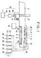
- Fig. 1 is a diagram which schematically illustrates an exemplary optical CVD system which can take advantage of the present invention;
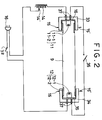
- Fig. 2 is a diagram which schematically illustrates an exemplary source of ultraviolet rays incorporating some of the features of the present invention;
- Fig. 3 is a diagram which shows the dependence of the thickness of silicon nitride films that are formed by use of an ultraviolet source according to the present invention on the distance between the irradiating window and the formed surface;
- Fig. 4 is a partial section view schematically showing the provision of an excess mercury reservoir in a source of UV rays according to the invention; and
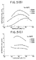
- Figs. 5(A) to 5(C) are graphical views showing the relationship between the temperature of the excess mercury in the reservoir of the UV source of Fig. 4 and the intensity of the ultraviolet rays.
- Making reference to the CVD system shown in Fig. 1,
substrates 1 which have formation surfaces are held by a holder 1' and are placed in areaction chamber 2. In the proximity of and above the substrates, there is provided ahalogen heater 3, the upper surface of which is cooled by means ofwater circulation conduits 32, within a heating chamber 3'. Below thereaction chamber 2 there is provided alight source chamber 5 which contains a large number ofultraviolet ray sources 9 that each consist of a low pressure mercury lamp of a type hereinafter described which receive electric energy from apower supply 13. Thelight source chamber 5 and the heating chamber 3' are held at approximately equal degrees of vacuum, each having a pressure difference of less than 1333.22 Pa (10 Torr) between the pressure of the reaction chamber 2'. For that purpose, a nonproduct gas (such as nitrogen, hydrogen, helium, or argon) is supplied from thegas source light source chamber 5 and to the heating chamber 3' through aflow meter 21 and avalve 22. - In Fig. 2 there is shown a low pressure arc discharge mercury lamp which incorporates features of the present invention and which serves as a source of ultraviolet rays used in the vapor phase reaction apparatus of Fig. 1. The low pressure arc
discharge mercury lamp 9 shown in Fig. 2 has a pair ofelectrodes - A
choke coil 14 is provided for impressing a voltage between the electrodes which is sufficient as an initial starting voltage, by shifting the phase by a small amount. First, aswitch 35 and aswitch 38 is turned on to cause a current to flow in the circuit and heat the filaments 11-1 and 12-1 in order to facilitate the emission of thermal electrons. Then, theswitch 35 is turned off, and an arc discharge is caused to take place between theelectrodes - Next, the inductance of the choke coil is reduced and the current that flows between the pairs of
electrodes terminals 37 are cooled by introducing a cooling medium intoenclosures inlets 15 and draining it from outlets 15', in order to cool theelectrodes - In general, for efficient electron emission, the filaments 11-1 and 12-1 should be coated with a material such as BaO which has a small work function. However, such a material has weak anti-shock properties and is easily destroyed by the collisions of atoms such as of argon and mercury. Because of this, electrodes 11-2 and 12-2 that are not coated with BaO are used as anti-shock electrodes, the electrodes 11-2 and 12-2 being electrically connected to the filaments 11-1 and 12-1 as will be appreciated by those skilled in the arc discharge tube art. In the present invention, the electrodes 11-2 and 12-2 are each in the form of a ring close to or adjacent to the inner wall of the
tube 9. The electrodes are forcibly cooled from outside of the tube, so that overheating of the electrodes 11-2 and 12-2 can be prevented and it becomes possible for the arc discharge to sustain a current which is about twice as large as that of the prior art. As a result, in spite of the large current it is possible to obtain a lamp life of at least close to 2,500 hours with the lamp output decreasing over this period by less than 10% of the initial lamp output. - Furthermore, in order to sufficiently improve the heat conductivity between the forced cooling means 33, 34 and the current lead-in
terminals 35 and the outer wall of the tube in the proximity of the electrodes, these parts are sealed to each other by means of a heat conductive paste. - With the above arrangement, it is possible to hold a maximum pressure by keeping the temperature rise within the tube at a value of 40°C, for example, of the design specifications. When in the vapor phase apparatus of Fig. 1 the source of
ultraviolet rays 9 itself is heated by the heat from theheater 3 for the substrate, it is of course effective to provide water cooling tubes that are disposed linearly beneath thetube 9 and close to each other. - In the case of manufacturing semiconductors such as silicon as a reaction product by means of the apparatus shown in Fig. 1, use may be made of silanes (SinH2n+2, N≧2) that are gases of silicides or silicon halides (HxSi₂F6-x(x=0-5), HxSi2C6-x(x=0-5), HxSi₃F8-x(x=0-8), HxSi₃C18-x(x=0-8), and the like as the product gases. In addition, use may be made of hydrogen, nitrogen, argon, or helium as a carrier gas for the nonproduct gases.
- In the case of manufacturing a nitride (silicon nitride, aluminium nitride, gallium nitride, indium nitride, antimony nitride, or the like) as a reaction product, use may be made respectively of Si₂H₆, A1(CH₃)₃, Ga(CH₃)₃, In(CH₃)₃, Sn(CH₃)₄, and Sb(CH₃)₃ as a reaction product, which is supplied from
gas source 23. In addition, as a nonproduct gas which participates in the reaction, use may be made of ammonia or hydrazine which is supplied fromgas source 26. Further, a nonproduct gas (hydrogen or helium) which does not participate in the reaction may be supplied fromsources - In the case of manufacturing an oxide (silicon oxide, phosphorus glass, boron glass, aluminum oxide, indium oxide, tin oxide, or their mixture) as a reaction product, use may be made of an oxide (N₂O,O₂, NO, or NO₂) as a product gas which participates in the reaction that is supplied from
gas source 26. In this case, a silicide (Si₂H₆, Si₂F₆, or Si₂C1₆), aluminum compound (A1(CH₃)₃) or Al(C₂H₅)₃), indium compound (In(CH₃)₃ or In(C₂H₅)₃), tin compound (Sn(CH₃)₄ or Sn(C₂H₅)₄) antimony compound (Sb(CH₃)₃ or Sb(C₂H₅)₃), respectively, may be made use of as a product gas which is supplied fromgas source 23. In addition, hydrogen or helium as a nonproduct gas which does not participate in the reaction may be supplied fromsource 24 as a carrier gas. Further, phosphine (PH₃) and diborane (B₂H₆) may be supplied fromsource 25. - In the case of manufacturing a conductor (aluminium, tungsten, molybdenum, tin, or a silicide of each), use may be made of hydrogen, argon, or helium as a nonproduct gas. In addition, Al(CH₃)₃, WF₆, W(C₂H₅)₅, MoC1₅, Mo(CH₃)₅, TiC1₄, Ti(CH₃)₄, or a mixture of each of these and SiH₄, Si₂F₆, SiH₂C1₂, or SiF₄, may be used respectively as a product gas, being supplied from
sources sources - Pressure control for the reaction chamber is accomplished by exhausting the gas through a turbo molecular pump (such as the PG550 pump manufactured by Osaka Vacuum Co., Ltd.) 18 and a
rotary pump 19 via acontrol valve 17 and acook 20. For pumping down areserve chamber 4 by theexhaust system 8, the reserve chamber side of theexhaust system 8 is opened and the reaction chamber side is closed by means of thecook 20. On the other hand, for pumping, or for causing photochemical reactions in, the reaction chamber, the reaction chamber side is opened and the reserve chamber side is closed. - In the process of film formation, a load and lock system which will not give rise to a pressure difference during transporation of a substrate from the reserve chamber to the reaction chamber may be adopted. First, the reserve chamber is pumped following insertion and dispostion of a
substrate 1 and a holder 1' in the reserve chamber. Then, thesubstrate 1 and the holder 1' are moved into thereaction chamber 2 which is pumped to a vacuum of 133.3 10⁻⁷Pa (10⁻⁷ Torr) or less by opening a gate valve 6 which is provided between the reserve and reaction chambers. Thereaction chamber 2 and thereserve chamber 4 are partitioned again by closing the gate valve 6. - Following that, a nonproduct gas is introduced into the light source chamber and the heating chamber at a flow-rate of 100 to 1,500 cc/min, in order to prevent mixing of reactive gases in the light source chamber due to reverse flow. At the same time, a nonproduct gas, for example NH₃, which participates in the reaction is supplied to the reaction chamber. The system is left standing in that state for about 30 minutes to cause photoetching of a formed surface of the substrate by active hydrogen and fluorine that are generated in the photodecomposition of the gases. With this arrangement, etching by irradiation becomes possible as a result of removal of oxides from the formed surface, leaving the surface nice and clean. Following that, a product gas selected from the available reactive gases is supplied to the reaction chamber through a
nozzle 30. - As a light source for enabling the photochemical reaction, use is made of low pressure arc discharge
mercury lamps 9 made of a synthetic quartz tube, and equipped with forced cooling means 33 and 34 as previously described. The source of ultraviolet rays might for example consist of 16 low pressure mercury lamps capable of emitting UV radiation at wavelengths of 185 nm and 254 nm, and having an emission length of 40 cm, an irradiation intensity of 60 to 100 mW/cm², and a lamp power of 150 to 500 W. - The ultraviolet rays from the source irradiate the
reaction gases 31 and the forming surface 1' of thesubstrate 1 in the reaction space of thereaction chamber 2, through atransparent covering plate 10 made of synthetic quartz. Theheater 3 is of "deposition up" type and is placed on the upper side of thereaction chamber 2. By such an arrangement, it is possible to avoid generation of a cause for creating pin holes through attachment of flakes on the forming surface. Thesubstrate 1 is heated by the halogen heater to a predetermined temperature in the range between room temperature and 700°C. The reaction chamber is made of stainless steel. The source of ultraviolet rays is housed in a light source chamber which is held in a vacuum. The light source chamber and the reaction chamber are held under a reduced atmosphere, surrounded by a stainless steel container. Because of this, it is possible with no technical difficulty to form a film on a large substrate of a size such as 30cm x 30cm instead of a small area of film formation of 5cm x 5cm. - In use of the apparatus of Fig. 1 in the formation of silicon nitride films, for example, ammonia was supplied from
source 25 at a rate of 200 cc/min and disilane was supplied fromsource 23 at a rate of 20 cc/min, as reactive gases. By setting the substrate temperature at 350°C, a result as shown by thecurve 40 of Fig. 3 was obtained. The substrate used was 4 wafers with diameter of 12.7 cm (5 inches). The pressure within the reaction chamber was 1333.22 Pa (10.0 Torr). As a nonproduct gas which does not participate in the reaction, nitrogen was introduced fromsource 27 at a flow rate of 200 cc/min. - With a reaction proceeding for 50 minutes, there were obtained silicon nitride films with thicknesses in the range of 1000 to 3500 Å. The intensity of ultraviolet rays of wavelength 185 nm on the forming surface was 40 mW/cm². The dependence of the thickness of the formed film on the distance between the covering
plate 10 and the substrate that has a formed surface is as shown by thecurve 40 in Fig. 3. It will be seen fromcurve 40 in Fig. 3 that a maximum thickness of 3,000Å was obtained for a 1cm distance between the upper surface of the window and the formed surface. It will be seen also that it is very important to have the distance less than 3cm, and preferably less than 2cm, in order to obtain a film thickness which is greater than 2,000Å. - As may be seen from
curve 39 in Fig. 3, when use is made of well-known conventional mercury lamps, instead of using mercury lamps of the forced cooling type hereinbefore described, the intensity of ultraviolet rays cannot be raised beyond 20 mW/cm². Because of this, the maximum thickness in this case was up to 1,000Å. (For the case of a distance of 1cm from the UV source to the substrate). - Referring now to Fig. 4, this illustrates how in a UV source according to the invention advantages can be obtained by cooling a mercury reservoir in which excess mercury is accumulated in the liquid phase. Fig. 4 is a sectional view of the reservoir which is provided on and projects from the synthetic quartz tube of the light source at a position near the end of the tube where plasma does not arise. Around the
reservoir 40 there is provided acooling device 41 with anoil layer 42 in between which makes thermal connection between thereservoir 40 and thecooling device 41. The cooling device is made from a substance having a high heat conductance such as aluminium, copper or so on, and is provided with a plurality of water conduits therethrough. The temperature of the liquid mercury in the reservoir can be adjusted by regulating the flow rate of cooling water circulating in the conduits with reference to the measured temperature of the mercury as determined by a temperature sensor (not shown in the figure) provided on the reservoir. - Figs. 5(A) to 5(C) show the relationship between the intensity of the light source of Fig. 4 versus the temperature of liquid mercury in the mercury reservoir with power supplies of 200W, 150W and 100W. "Ta" indicates the temperature of the tube environment, namely, the temperature of the tube of the light source. As shown in Fig. 5(A), the highest intensity can be obtained at about 60°C liquid mercury tempeature when input power is 200W and the lamp environment temperature is 100°C. When the temperature of the lamp environment is 200°C, the optimum temperatures are clearly seen from Fig. 5(B) for each input power level. The optimum temperatures, however, become unclear at 300°C lamp environment temperature as shown in Fig. 5(C). It should be understood that these figures are only examples and if one desires to know the optimum temperature to which the mercury reservoir should be cooled, then one should examine the situation for each particular case. With the configuration shown in Fig. 4, the pressure of mercury vapor in the tube is determined not by the lamp temperature but by the temperature of the mercury in the reservoir which is controlled by the cooling device.
- As should be clear from the foregoing description, the present invention enables films to be successfully formed on substrates of large area by reducing consumption of electrodes of low pressure mercury lamps and by passing a large current in the lamp. As a result, it has been found possible to increase the limiting film thickness from the conventional value of 1,000Å to a value which is greater than 3,000Å. In addition, by applying a high frequency of 100 Hz to 1 kHz to the mercury lamps, and by adjusting its power factor, it was found possible to increase the emission intensity of the radiation of 185 nm wavelength. Further, according to the present invention, it is possible to obtain a maximum film thickness by choosing the distance between the transparent covering plate and the substrate surface at a value of 3cm or less, preferably 0.3 to 2cm. The present invention has made it possible to produce excellent silicon nitride films that possess interface level density of less than 3x10¹¹cm⁻².
- In the foregoing the present invention was described in conjunction with the formation of silicon nitride films. However, various films of semiconductors, insulators, conductors, and others such as amorphous silicon films, silicon oxide films, phosphorus glass which contains these substances along with added impurities, boron glass, or aluminum, can be formed by the use of the same technical ideas. In addition, it is effective to form passivation films on iron, nickel, cobalt, or magnetic substances of their compounds, by the use of carbonyl compounds of iron, nickel, or cobalt that has not been touched upon in the foregoing as a reactive gas.
- It should also be mentioned that a dopant may also be added in the formation of silicon semiconductors in the experimental example.
- In addition, if environmental pollution could be disregarded, the speed of film growth may be improved by passing the reactive gases through a mercury bubbler.
- In Fig. 1, the light source was placed in the lower part and the reaction space was provided in the upper part of the system. However, if flakes that are generated can be removed with reasonal ease, then the dispostion of the substrate can be facilitated by providing the reaction space in the lower part, contrary to the present embodiment. In addition, the light source may be disposed at the side of the apparatus if so desired.
- The present invention is not limited to the specific embodiments explained above and many modifications and variations will occur to those skilled in the art without departing from the scope of the invention. For instance, the source of ultraviolet rays may be effectively applied to photo-etching systems or other technical fields besides its application to chemical vapor deposition (CVD).
Claims (6)
- A low pressure ultraviolet source comprising:
a discharge tube (9);
anode and cathode electrodes (11, 12) provided in said tube for establishing an electrical discharge therein at a discharge region defined between said electrodes;
a reservoir (40) communicating with said tube at a location spaced from the heat developed at said discharge region;
means (41) associated with said reservoir for controlling the temperature thereof; and
an active substance in said reservoir in liquid form and with vapour of said substance filling the discharge region so as to emit ultraviolet radiation when excited by an electric discharge between said electrodes; wherein
the amount of said active substance, that is contained in liquid form in said reservoir, is such that the vapour pressure of said vaporous substance within the tube is the saturated vapour pressure of the temperature-controlled liquid substance in the reservoir and is determined by the temperature of the reservoir and not by the operating temperature of the discharge tube. - An ultraviolet source as claimed in claim 1 wherein said active substance is mercury.
- An ultraviolet source as claimed in claim 1 or 2 wherein means (15) are provided for cooling said electrodes (11, 12).
- A photochemical apparatus including a low pressure ultraviolet source as claimed in any preceding claim.
- An optical CVD system including a low pressure ultraviolet source as claimed in any of the preceding claims 1-3.
- A method of operating a photochemical apparatus as claimed in claim 4 or an optical CVD system as claimed in claim 5, in accordance with which the temperature of the active substance in the reservoir of the ultraviolet source is adjusted in order to obtain optimum output intensity from the source and the vapour pressure of said substance within the discharge tube of the ultraviolet source is the saturated vapour pressure of the temperature-controlled liquid substance in the reservoir and is determined by the temperature of the reservoir and not by the operating temperature of the discharge tube.
Applications Claiming Priority (4)
| Application Number | Priority Date | Filing Date | Title |
|---|---|---|---|
| JP65515/86 | 1986-03-24 | ||
| JP61065515A JPS62222072A (en) | 1986-03-24 | 1986-03-24 | Ultraviolet light source and photochemical reaction process |
| JP226449/86 | 1986-09-24 | ||
| JP61226449A JPS6380463A (en) | 1986-09-24 | 1986-09-24 | Optical source por light processing device and its using method |
Publications (2)
| Publication Number | Publication Date |
|---|---|
| EP0239374A1 EP0239374A1 (en) | 1987-09-30 |
| EP0239374B1 true EP0239374B1 (en) | 1992-01-22 |
Family
ID=26406664
Family Applications (1)
| Application Number | Title | Priority Date | Filing Date |
|---|---|---|---|
| EP87302553A Expired - Lifetime EP0239374B1 (en) | 1986-03-24 | 1987-03-24 | Source of ultraviolet rays and use of the same in photochemical reaction methods |
Country Status (5)
| Country | Link |
|---|---|
| US (1) | US4949004A (en) |
| EP (1) | EP0239374B1 (en) |
| KR (1) | KR900009084B1 (en) |
| CN (1) | CN1009883B (en) |
| DE (1) | DE3776170D1 (en) |
Families Citing this family (10)
| Publication number | Priority date | Publication date | Assignee | Title |
|---|---|---|---|---|
| DE3840577A1 (en) * | 1988-12-01 | 1990-06-07 | Patent Treuhand Ges Fuer Elektrische Gluehlampen Mbh | DISCHARGE VESSEL FOR A HIGH PRESSURE DISCHARGE LAMP AND METHOD FOR THE PRODUCTION THEREOF |
| US4994705A (en) * | 1989-03-27 | 1991-02-19 | Hughes Aircraft Company | Water-cooled, low pressure gas discharge lamp |
| JPH04109952A (en) * | 1990-08-31 | 1992-04-10 | Toshiba Lighting & Technol Corp | Ultraviolet(uv) applying device |
| US5972743A (en) * | 1996-12-03 | 1999-10-26 | Advanced Technology Materials, Inc. | Precursor compositions for ion implantation of antimony and ion implantation process utilizing same |
| ES2201499T3 (en) * | 1997-03-21 | 2004-03-16 | Patent-Treuhand-Gesellschaft Fur Elektrische Gluhlampen Mbh | GASEOUS DISCHARGE LAMP WITH DIELECTRICALLY INHIBITED ELECTRODES. |
| DE10201617C5 (en) * | 2002-01-16 | 2010-07-08 | Wedeco Ag Water Technology | Amalgam-doped low-pressure mercury UV emitter |
| DE10349237A1 (en) * | 2003-10-20 | 2005-05-12 | Wedeco Ag | Spotlight unit with position adjustable spotlight |
| US6924495B1 (en) * | 2004-02-13 | 2005-08-02 | James Lawrence Brickley | Heat controlled ultraviolet light apparatus and methods of sanitizing objects using said apparatus |
| DE102006023870B3 (en) * | 2006-05-19 | 2007-06-28 | Heraeus Noblelight Gmbh | Mercury-low pressure-amalgam lamp arrangement, has lamp which is enclosed by polytetrafluoroethylene strip in region of amalgam storage, where strip forms mechanical contact to cladding tube |
| JP6254516B2 (en) * | 2014-12-19 | 2017-12-27 | 東京エレクトロン株式会社 | Substrate processing apparatus and substrate processing method |
Citations (1)
| Publication number | Priority date | Publication date | Assignee | Title |
|---|---|---|---|---|
| EP0173962A2 (en) * | 1984-09-05 | 1986-03-12 | Patent-Treuhand-Gesellschaft für elektrische Glühlampen mbH | Compact low-pressure discharge lamp |
Family Cites Families (3)
| Publication number | Priority date | Publication date | Assignee | Title |
|---|---|---|---|---|
| US3983385A (en) * | 1974-08-23 | 1976-09-28 | Union Carbide Corporation | Method and apparatus for operating a mercury vapor lamp |
| US4295074A (en) * | 1979-03-21 | 1981-10-13 | Rca Corporation | Mercury arc lamp having communicating mercury reservoir |
| US4615294A (en) * | 1984-07-31 | 1986-10-07 | Hughes Aircraft Company | Barrel reactor and method for photochemical vapor deposition |
-
1987
- 1987-03-23 KR KR1019870002635A patent/KR900009084B1/en not_active Expired
- 1987-03-24 CN CN87102347A patent/CN1009883B/en not_active Expired
- 1987-03-24 DE DE8787302553T patent/DE3776170D1/en not_active Expired - Lifetime
- 1987-03-24 EP EP87302553A patent/EP0239374B1/en not_active Expired - Lifetime
-
1989
- 1989-02-08 US US07/307,190 patent/US4949004A/en not_active Expired - Fee Related
Patent Citations (1)
| Publication number | Priority date | Publication date | Assignee | Title |
|---|---|---|---|---|
| EP0173962A2 (en) * | 1984-09-05 | 1986-03-12 | Patent-Treuhand-Gesellschaft für elektrische Glühlampen mbH | Compact low-pressure discharge lamp |
Also Published As
| Publication number | Publication date |
|---|---|
| KR870009249A (en) | 1987-10-24 |
| DE3776170D1 (en) | 1992-03-05 |
| KR900009084B1 (en) | 1990-12-20 |
| US4949004A (en) | 1990-08-14 |
| CN87102347A (en) | 1987-09-30 |
| EP0239374A1 (en) | 1987-09-30 |
| CN1009883B (en) | 1990-10-03 |
Similar Documents
| Publication | Publication Date | Title |
|---|---|---|
| US4724159A (en) | Conductive layer deposition method with a microwave enhanced CVD system | |
| US5183511A (en) | Photo CVD apparatus with a glow discharge system | |
| US6230650B1 (en) | Microwave enhanced CVD system under magnetic field | |
| US4927786A (en) | Process for the formation of a silicon-containing semiconductor thin film by chemically reacting active hydrogen atoms with liquefied film-forming raw material gas on the surface of a substrate | |
| US5221561A (en) | Process for the photochemical treatment of a material using a flash tube light source | |
| US6113701A (en) | Semiconductor device, manufacturing method, and system | |
| US20040134429A1 (en) | Film forming method and film forming apparatus | |
| EP0645793B1 (en) | Electron emitting device | |
| US4910436A (en) | Wide area VUV lamp with grids and purging jets | |
| EP0239374A1 (en) | Source of ultraviolet rays and use of the same in photochemical reaction methods | |
| US4069492A (en) | Electroluminescent semiconductor device having a body of amorphous silicon | |
| US5036373A (en) | Electric device with grains and an insulating layer | |
| JPH0143449B2 (en) | ||
| US4910044A (en) | Ultraviolet light emitting device and application thereof | |
| US5952061A (en) | Fabrication and method of producing silicon films | |
| US6218300B1 (en) | Method and apparatus for forming a titanium doped tantalum pentaoxide dielectric layer using CVD | |
| Madan et al. | High deposition rate amorphous and polycrystalline silicon materials using the pulsed plasma and “Hot-Wire” CVD techniques | |
| KR920000591B1 (en) | Microwave enhanced cvd system | |
| US5139970A (en) | Electric device and manufacturing method of the same | |
| EP0227839A1 (en) | Method of forming a thin film | |
| EP0413595A2 (en) | Method of manufacturing electric devices | |
| JP2564538B2 (en) | Semiconductor processing equipment | |
| JP2608456B2 (en) | Thin film forming equipment | |
| Ueno et al. | Highly efficient generation of high-energy photons and low-temperature oxidation of a crystal silicon surface with O1D radicals | |
| JPS6380463A (en) | Optical source por light processing device and its using method |
Legal Events
| Date | Code | Title | Description |
|---|---|---|---|
| PUAI | Public reference made under article 153(3) epc to a published international application that has entered the european phase |
Free format text: ORIGINAL CODE: 0009012 |
|
| AK | Designated contracting states |
Kind code of ref document: A1 Designated state(s): AT BE CH DE ES FR GB GR IT LI LU NL SE |
|
| RBV | Designated contracting states (corrected) |
Designated state(s): DE FR GB |
|
| 17P | Request for examination filed |
Effective date: 19880315 |
|
| 17Q | First examination report despatched |
Effective date: 19890419 |
|
| RAP1 | Party data changed (applicant data changed or rights of an application transferred) |
Owner name: SEMICONDUCTOR ENERGY LABORATORY CO., LTD. |
|
| GRAA | (expected) grant |
Free format text: ORIGINAL CODE: 0009210 |
|
| AK | Designated contracting states |
Kind code of ref document: B1 Designated state(s): DE FR GB |
|
| REF | Corresponds to: |
Ref document number: 3776170 Country of ref document: DE Date of ref document: 19920305 |
|
| ET | Fr: translation filed | ||
| PLBE | No opposition filed within time limit |
Free format text: ORIGINAL CODE: 0009261 |
|
| STAA | Information on the status of an ep patent application or granted ep patent |
Free format text: STATUS: NO OPPOSITION FILED WITHIN TIME LIMIT |
|
| 26N | No opposition filed | ||
| PGFP | Annual fee paid to national office [announced via postgrant information from national office to epo] |
Ref country code: FR Payment date: 19930309 Year of fee payment: 7 |
|
| PGFP | Annual fee paid to national office [announced via postgrant information from national office to epo] |
Ref country code: GB Payment date: 19930312 Year of fee payment: 7 |
|
| PGFP | Annual fee paid to national office [announced via postgrant information from national office to epo] |
Ref country code: DE Payment date: 19930324 Year of fee payment: 7 |
|
| PG25 | Lapsed in a contracting state [announced via postgrant information from national office to epo] |
Ref country code: GB Effective date: 19940324 |
|
| GBPC | Gb: european patent ceased through non-payment of renewal fee |
Effective date: 19940324 |
|
| PG25 | Lapsed in a contracting state [announced via postgrant information from national office to epo] |
Ref country code: FR Effective date: 19941130 |
|
| PG25 | Lapsed in a contracting state [announced via postgrant information from national office to epo] |
Ref country code: DE Effective date: 19941201 |
|
| REG | Reference to a national code |
Ref country code: FR Ref legal event code: ST |