EP0226325A1 - Détection de signalisation - Google Patents
Détection de signalisation Download PDFInfo
- Publication number
- EP0226325A1 EP0226325A1 EP86308733A EP86308733A EP0226325A1 EP 0226325 A1 EP0226325 A1 EP 0226325A1 EP 86308733 A EP86308733 A EP 86308733A EP 86308733 A EP86308733 A EP 86308733A EP 0226325 A1 EP0226325 A1 EP 0226325A1
- Authority
- EP
- European Patent Office
- Prior art keywords
- signalling data
- dial pulse
- dial
- received signal
- detecting
- Prior art date
- Legal status (The legal status is an assumption and is not a legal conclusion. Google has not performed a legal analysis and makes no representation as to the accuracy of the status listed.)
- Granted
Links
Images

Classifications
-
- H—ELECTRICITY
- H04—ELECTRIC COMMUNICATION TECHNIQUE
- H04Q—SELECTING
- H04Q1/00—Details of selecting apparatus or arrangements
- H04Q1/18—Electrical details
- H04Q1/30—Signalling arrangements; Manipulation of signalling currents
- H04Q1/32—Signalling arrangements; Manipulation of signalling currents using trains of dc pulses
Definitions
- This invention relates to detection of signalling data such as dial pulse signalling data.
- dial pulse signalling data means the make and break signals commonly produced by telephone dials, the pushbutton equivalent or the like and used in telecommunications systems for control and routing of calls through the telecommunications network.
- the present invention provides a method and apparatus for detecting dial pulse signalling data which can be both flexible and reliable in use.
- a method of detecting dial pulse signalling data in a received signal comprising a training process and a recognition process, wherein the training process comprises processing of a portion of the received signal to extract characteristics of the received signal and said recognition process uses said characteristics to assist in detecting dial pulse signalling data in the received signal.
- a detector for dial pulse signalling data comprising means for processing a portion of a received signal to extract characteristics of the received signal and operable using said characteristics to assist in detecting dial pulse signalling data in the received signal.
- interactive terminal equipment comprising a detector for detecting digits dialled, said equipment being adapted to transmit messages to the user inviting the user to dial digits according to the users requirements and to provide a service to the user dependent on the digits dialled.
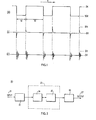
- Figure 1 shows idealised versions of the electrical waveforms of analogue dial pulse signals.
- Figure l(a) shows a portion of dial pulse signalling in its relatively distortion free state before entering a dc block (ie before reaching the first relay set of transmission bridge in the local exchange).
- Time interval t 1 represents a make period and interval t 2 represents a break period.
- the make/break period t 3 is therefore made up of the sum of the two periods t 1 + t2.
- Make period t 1 is nominally 33 1/3 ms and break period t 2 nominally 66 2/3 ms, thus giving rise to a make/break period t 3 of 100 ms corresponding to a mean dial pulse signalling rate of 10 impulses per second (ips).
- dial signalling rates may be allowed to vary from 7 to 12 ips thus altering the make/break pulse period t 3 .
- Any given dial will produce relatively constant values for periods t 1 ana t 2 but this will vary from dial to dial and from one line to another.
- Figure 1(b) shows the effect of passing the signals of Figure l(a) through a first transmission bridge (a dc tlock).
- Figure l(c) shows idealised ringing distortion due to passing the signal of Figure 1(b) along a transmission medium. It shculd be noted that the wave forms of Figures 1(a) - 1(c) and in particular Figure l(c) will normally be subject to additional random oistortion effects (not shown) of background noise and impulsive interference.
- a dial pulse detection system 20 is shown in which analogue dial pulses of the type shown in Figures 1(a) or l(b) or 1(c) are input at 21 to an input interface 22.
- the analogue dial pulses are then passed to a detector 23.
- the detector 23 comprises an analogue to digital converter 24 and a microprocessor system 25.
- the converter 24 converts the analogue dial pulses into digital samples which can be read by the microprocessor 25.
- Processed output from detector 23 passes via interface 26 and is output at 27.
- Input and output interfaces (22,26) ensure that all signal levels are compatible and provide protection for detector 23.
- Input interface 22 also includes a low pass filter (not shown) in order to remove unwanted higher frequency components in the received signal and thereby aid detection.
- dial pulse detector of Figure 2 would normally be located at a distant receiving end on a telecommunications line.
- a user would therefore be able to route his call through the exchange equipment (having dialled the required number in the normal fashion) and would then be able to supply extra dialled digits over the established link to the detector.
- the detector may therefore be used to detect this dialled signalling information which may in turn be used for control of other equipment to provide a required service to the user.
- dialled digits may be used to control computerised data bases; for implementing automatic operator facilities for PABXs; and in interactive answering machine systems.
- a typical automatic operator application of the invention in a PABX system would enable an outside exchange line user to dial any extension on the PABX.
- the detection system 20 would, for example, be located in or before the PABX.
- a telephone call for the PABX would be intercepted by the detection system which would then play a message to the caller.
- the detection system would detect additional digits dialled by the user, i.e. the extension number, and pass the detected number on to the PABX equipment to route the call through to the required extension. In a preferred embodiment of the invention, this would be achieved by the user dialling the extension number preceded by a training digit with a long pulse train (e.g. a nine).
- the invention may also be easily incorporated in systems requiring interactive detection of dial pulse signalling data and one example of such a system would be an intelligent controller for accessing a computerised data base.
- the intelligent controller would send instructions over the exchange line to the user (e.g. to access file X dial 123) who would then respond by dialling the appropriate digits.
- the dial pulse detection system 20 would then pass the detected digits to the controller in order to initiate the appropriate action.
- security of access could be achieved by ensuring that each user dials a unique number for access to the data base
- the type of dial pulse signalling available to the detector will be of the form shown in Figure l(c).
- the regular loop/disconnect (make/break) pulses of Figure l(a) have been degraded by the transmission bridge and the characteristics of the line into a series of positive and negative going oscillations which decay in time. These oscillations are excited by the transients of Figure 1(b) which correspond to the rising and falling edges of the original loop/disconnect signal of Figure l(a).
- the signal of Figure l(c) will also contain noise (not shown) which may take the form of both random impulsive interference (mostly due to crosstalk from other lines carrying dial pulses) and general background noise.
- the amplitude of the signal of Figure 1 (c) typically varies greatly with a mean peak level of approximately 2 volts and a standard deviation of approximately 1.5 volts.
- Background noise typically ranges from 50 mV - 100 mV with impulsive noise often reaching much larger levels.
- Input buffer 22 is designed to cope with the above variation in input signal level.
- Input buffer 22 incorporates a low pass filter in order to reject the unwanted higher frequency components (primarily above 4kHz) present in the received signal. This low pass filter band limits the received signal to 4kHz thereby retaining the main part of the signalling information and enabling the subsequent use of an 8 kHz sampling frequency. Additionally, since most of the signalling information is conveyed at frequencies below 2 khZ, removal of higher frequencies by a second low pass filter serves to improve the subsequent detection process (described below). These filtering operations could be combined into one operation.
- Buffer 22 incorporates gain control circuitry which serves to provide an optimum signal level for operation of the detector 23 and also protects the detector 23 from damage arising from any excessively large voltage transients at the input 21. Buffer 22 also provides dc isolation of the detector 23 from the telephone line at input 21.
- the analogue signal then passes to the analogue to digital converter (ADC) 24.
- ADC 24 is a conventional device which produces digital codes compatible with the input of processor 25. In the present implementation standard A-law encoding is used. However, since maximum negative going peaks in the analogue signal (due to the falling edge of the long break pulse) tend to be larger than any positive going peaks, a digital encoding technique is used which full wave rectifies the received signal by taking magnitude of the received signal as a positive modulus. All analogue voltages are therefore encoded as digital samples having a positive modulus.
- the samples produced by ADC 24 are then made available for processing by the microprocessor system 25. Processor 25 operates on the samples in two distinct modes to achieve detection of the dial pulse signalling data. The first mode is a training process, and the second mode is a recognition process.
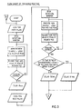
- FIG. 3 is a flow chart of the operation of the training process.
- the purpose of this training process is to obtain a "signature" or template of various signal parameters relating to the dialling instrument to which the detector is to be trained. For this reason, the user would (after a connection to the detector has been established) dial a predetermined digit intended solely for the purpose of training the detector to that dial and line.
- the training digit is a nine which gives rise to a train of 9 make/break pulses, giving the detector a good opportunity to train to the signal parameters of the dial and the line.
- telephone instruments produce extra pulses at the beginning and end of dialling. These are termed “off-normal" pulses and are caused by the switching between voice and dial signalling circuitry within the telephone, and occur as single pulses before and after the make/break pulse sequence.
- Figure 3 shows this training process, in which a template of the parameters of the dial and line is formed using measured signal levels and times.
- the processor 25 analyses the digital samples from ADC 24 which represent the received signal.
- Processor 25 looks for those samples representing a first maximum peak whereupon a detection window is held open for 9 ms. All samples received while this window is open are analysed and a maximum peak level occuring within this period is recorded. The window is then closed, and there is a delay of 19 ms before any further samples are taken. Following this, another window is opened on detection of the next peak and a maximum peak level obtained within this period is again recorded.
- Processor 25 calculates the time between these maximum peaks and this parameter is stored.
- this time is found to be less than 53 ms, then this is taken to indicate that the interval between the previous two peaks constituted a make period (i.e. t I ideally 33 3 ms as in Figure 1). There is then a delay of 50 ms before beginning the next analysis in order to await the arrival of the peak representing the end of the subsequent break period (and the beginning of the next make period). Should that time period between the first two peaks be found to be greater than 53 ms, thus indicating the occurrence of a break period (i.e.
- processor 25 will generate an error signal (which could be in the form of a tone or a standard voice synthesised message) to indicate to the user that there has been a malfunction and that the user shoula re-dial.
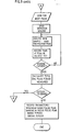
- processor 25 begins the recognition process once the training process has been successfully completed. The operation of the recognition process is shown in Figures 4 and 5.
- the recognition process uses the dial pulse characteristics obtained in the training process to set up a series of analysis windows. Any samples received outside these windows are ignored.
- the advantage of setting up these analysis windows according to the dial pulse information from the training process is that the width of each window can be made small (9 ms in this example) in comparison to the dial pulse period (an average of 100 ms). In this way only small amounts of signal need be analysed at any one time in order to be certain of receiving valid dial pulses in the presence of impulsive noise.
- Figure 4 illustrates the time format 40 of the analysis windows 42 observed by processor 25 after the first make pulse 41 has been received (corresponding to the first pulse of the digits which are to be detected after the training digit).
- Each analysis window 42 is associated with a location 51 in the pulse-array 50 (of Figure 5) which is built up progressively and stored by processor 25 to describe the incoming pulse train.
- the analysis windows 42 are numbered from 0 to 24 where the first window is numbered 0.
- Figure 4 shows an expanded view of windows 8, 9 and 10. This numbering of the windows 42 corresponds to the numbered locations 51 in the array 50 of Figure 5.
- Each location 51 of array 50 stores the result of its correspondingly numbered analysis windows 42.
- Pulse array 50 corresponds to an example recognition of the dialled digit six.
- the analysis windows 42 are opened at regular intervals corresponding to the measured make and break periods (t l and t 2 respectively) from the training process. While each analysis window 42 is open, and this is only for a period of 9 ms, processor 25 compares the amplitude of received samples against the appropriate make or break peak value expected for that particular dial (from the training process). If the amplitude of a sample is found to fall within an acceptable tolerance of the expected peak value, then a valid pulse is determined to have been received, and the correspondingly numbered location in the pulse array 50 of Figure 5 is flagged true. If an analysis window 42 should time out with no valid pulse being received, then the corresponding element of the pulse array 50 is flagged false. Array 50 of Figure 5 shows each location 51 flagged in this way, either with a 1 (i.e. true), or an F (i.e. false).
- processor 25 causes a delay until the next analysis window 42 is due to be opened, where this delay is determined by the appropriate measured t l or t 2 pulse period from the training process.
- All even numbered locations (0,2,4,6 ...) in array 50 will hold a true or false result representing a valid or invalid make pulse received (this being so since it is assumed that the first pulse received must be a make pulse).
- All odd numbered locations (1,3,5,7,...) in array 50 will hold a true or false result representing a valid or invalid break pulse received.
- Locations (0,1) therefore represent the first dial pulse digit received (i.e. one make and one break), with locations (2,3) representing the second dial pulse received, and so on.
- Processor 25 causes the analysis windows 42 to be opened and closed according to the format 40 of Figure 4, until any of the following conditions are determined to be true:
- processor 25 operates a missed pulse counter which is incremented on every failure to recognise a valid pulse in each analysis window.
- Processor 25 resets this missed pulse counter on each occurrence of two consecutive correctly received pulses, under the assumption that noise spikes, being essentially random in nature, are unlikely to cause this effect and processor L5 therefore determines that, since the pulse train is still being received, all previous missed pulses were mistakes. Errors will also be detected which arise from any pulses being received in windows 20 to 24 (area 43 in Figure 4) which cause any of locations 20 to 24 to be flagged true. Processor 25 therefore determines that such locations flagged true must be due to noise since no valid digits greater than the digit zero can be received.
- processor 25 determines the value of the received digit by searching backward through the pulse array for the first occurrence of two consecutive correctly received pulses which correspond tc a valid digit received. It then calculates the number dialled from the position in the array that this occurs.
- Figure 5 shows one example of the state of the pulse array 50 after reception of the dialled digit 6 where locations (10, 11) hold the last consecutively valid entries which correspond to the dialled digit 6.
- 52 of Figure 5 shows location 3 which is the first to be flagged false.
- the missed pulse counter operated by processor 25 therefore records one missed pulse.
- Processor 25 searches the array 50 by working back from 55 (location 17 - the last one flagged) to find the first instance of consecutive valid pulses (i.e. flagged true). In this example this first occurs at 54 (locations 10 and 11). Since locations 10 and 11 correspond to the dialled digit six, processor 25 determines that the dialled digit was in fact a six and no further locations are searched. In this example, if location 12 was also true, and 13 false, then the dialled number would still be recognised as a six (with the location 13 being ignored as a single error pulse). This condition will also prevent an "off-normal" pulse (which occurs after the dialling pulses) being treated as a dial pulse.
- This "off-normal" pulse occurs at approximately one break period after the last make dial pulse transient and thus could be recognised as a valid break pulse transient. If location 12 was false and locations 13 and 14 true then the digit received would still be recognised as a six since the rule of two consecutive true locations implying a valid pulse period can only apply in locations corresponding to a digit value (i.e 0 and 1, 2 and 3, 4 and 5... etc.) and not in locations falling between digit values (i.e 1 and 2, 3 and 4, etc).
- the recognition process therefore employs error detection and correction embodied in the missed pulse counter and its reset by processor 25 according to the above conditions.
- processor 25 If, for some reason, it is not possible for processor 25 to perform a satisfactory recognition process (as in, for example, condition 4 above) then the processor will cause a malfunction signal to be sent to the user in the form of a tone or a voice synthesised message in order that the user will understand that the number is to be redialled.
- processor 25 passes its numerical value to output buffer 26 (shown in Figure 2) where it is made available at the output 27 for use by other equipment as described above. Processor 25 is then ready to repeat the recognition process on any subsequent digits dialled by the user. When all digits have been successfully received, processor 25 will also cause a voice synthesised message to be sent to the user to confirm the value of the dialled digits received and stored in buffer 26.
- the training process is carried out on a predetermined training digit which is used solely for training purposes and is not intended to be recognised by the system.
- the training process could be "implicit" and form part of the recognition process thus obviating the need for a separate training digit.
- the first digit would be used to train the detector to the dialling instrument, but would at the same time be itself recognised by the detector as well as being used as a basis for recognition of subsequent digits.
- This implicit training would require the first attempt at recognition to have the widest tolerances on pulse parameters which would have to be according to an average or optimum setting based on experience. Subsequent dialled digits would, however, be recognised according to a template prepared from the measured parameters of the first digit received.
- dial pulses may be extracted from the dial pulses during training to assist in detection.
- One such parameter is the polarity of the first peak in the transient which indicates whether a transient was generated by a make or break pulse.
- the number of zero crossings in the ringing of the transient i.e. the number of oscillations could be used to improve immunity against noise.
- Another option is to analyse the received signal between the detection windows to compare the level of the signal with the level of the make or break pulses measured during training.
- the detector can be made to ignore continuous signals such as speech which could otherwise cause false recognition.
- dial pulse detection system which performs analogue to digital conversion of the received analogue signal in order to process the signal in digital form, it is of course operable without such conversion in situations (such as in a wholly digital network) where the detector can be directly presented with the signal in digital form.
- Such measures can be taken to improve the performance of the detector 25 when dealing with received signals known to have a very poor signal to noise ratio.
- Such measures may include the use of additional signal pre-processing at the input buffer stage 22. This pre-processing could take the form of analogue or digital filters to enhance the signal to noise ratio of the received signal and thus provide for optimum operation of the detector.
Priority Applications (1)
| Application Number | Priority Date | Filing Date | Title |
|---|---|---|---|
| AT86308733T ATE51119T1 (de) | 1985-11-25 | 1986-11-10 | Signalisierungsdetektion. |
Applications Claiming Priority (2)
| Application Number | Priority Date | Filing Date | Title |
|---|---|---|---|
| GB8528951 | 1985-11-25 | ||
| GB858528951A GB8528951D0 (en) | 1985-11-25 | 1985-11-25 | Signalling detection |
Publications (2)
| Publication Number | Publication Date |
|---|---|
| EP0226325A1 true EP0226325A1 (fr) | 1987-06-24 |
| EP0226325B1 EP0226325B1 (fr) | 1990-03-14 |
Family
ID=10588721
Family Applications (1)
| Application Number | Title | Priority Date | Filing Date |
|---|---|---|---|
| EP86308733A Expired - Lifetime EP0226325B1 (fr) | 1985-11-25 | 1986-11-10 | Détection de signalisation |
Country Status (9)
| Country | Link |
|---|---|
| US (1) | US4924501A (fr) |
| EP (1) | EP0226325B1 (fr) |
| JP (1) | JP2673295B2 (fr) |
| AT (1) | ATE51119T1 (fr) |
| CA (1) | CA1265275A (fr) |
| DE (1) | DE3669633D1 (fr) |
| ES (1) | ES2014419B3 (fr) |
| GB (1) | GB8528951D0 (fr) |
| GR (1) | GR3000384T3 (fr) |
Cited By (4)
| Publication number | Priority date | Publication date | Assignee | Title |
|---|---|---|---|---|
| EP0295855A2 (fr) * | 1987-06-19 | 1988-12-21 | Comcheq Services Limited | Récepteur d'impulsions de sélection de cadran |
| EP0351445A1 (fr) * | 1986-11-18 | 1990-01-24 | Aerotel, Limited | Détecteur d'impulsions pour compter des impulsions générées par cadran |
| US5218636A (en) * | 1991-03-07 | 1993-06-08 | Dialogic Corporation | Dial pulse digit detector |
| FR2702114A1 (fr) * | 1993-02-23 | 1994-09-02 | Ferma | Procédé et installation d'analyse d'une suite de réponses impulsionnelles, notamment pour la reconnaissance de surnumérotation décimale à travers le réseau téléphonique. |
Families Citing this family (28)
| Publication number | Priority date | Publication date | Assignee | Title |
|---|---|---|---|---|
| JPS6441597A (en) * | 1987-08-07 | 1989-02-13 | Takeshige Fujitani | Method for detecting dial pulse |
| JP2843583B2 (ja) * | 1988-12-23 | 1999-01-06 | アエロテル リミテッド | パルス検出システム及びパルス検出方法 |
| CA2022750A1 (fr) * | 1990-08-07 | 1992-02-08 | Michel Ponton | Methode et dispositif de reconnaissance de signatures d'impulsion de numerotation |
| US5319702A (en) * | 1992-07-29 | 1994-06-07 | Tele-Matic Corporation | Method and apparatus for detecting and responding to hook flash events occurring on a remote telephone |
| US5428662A (en) * | 1993-03-01 | 1995-06-27 | Dialogic Corporation | Detecting make-break clicks on a telephone line |
| US5579387A (en) * | 1994-06-30 | 1996-11-26 | Winbond Electronics Corporation | Apparatus for accessing function code in telephone |
| KR0149765B1 (ko) * | 1995-11-10 | 1998-11-02 | 김광호 | 기계식 전화기 가입자의 페이징 서비스를 위한 클릭펄스 검출기 및 검출방법 |
| US5805685A (en) * | 1995-11-15 | 1998-09-08 | Gateway Technologies, Inc. | Three way call detection by counting signal characteristics |
| US5796811A (en) * | 1995-11-15 | 1998-08-18 | Gateway Technologies, Inc. | Three way call detection |
| US5881146A (en) * | 1996-02-05 | 1999-03-09 | Dialogic Corporation | Method and apparatus for determining digits dialed using a selected algorithm |
| US7110525B1 (en) | 2001-06-25 | 2006-09-19 | Toby Heller | Agent training sensitive call routing system |
| US7505406B1 (en) | 2001-07-13 | 2009-03-17 | Evercom Systems, Inc. | Public telephone control with voice over internet protocol transmission |
| US7899167B1 (en) | 2003-08-15 | 2011-03-01 | Securus Technologies, Inc. | Centralized call processing |
| US8000269B1 (en) | 2001-07-13 | 2011-08-16 | Securus Technologies, Inc. | Call processing with voice over internet protocol transmission |
| US7023979B1 (en) | 2002-03-07 | 2006-04-04 | Wai Wu | Telephony control system with intelligent call routing |
| US7372952B1 (en) | 2002-03-07 | 2008-05-13 | Wai Wu | Telephony control system with intelligent call routing |
| US7916845B2 (en) | 2006-04-13 | 2011-03-29 | Securus Technologies, Inc. | Unauthorized call activity detection and prevention systems and methods for a Voice over Internet Protocol environment |
| US7860222B1 (en) | 2003-11-24 | 2010-12-28 | Securus Technologies, Inc. | Systems and methods for acquiring, accessing, and analyzing investigative information |
| US9020114B2 (en) | 2002-04-29 | 2015-04-28 | Securus Technologies, Inc. | Systems and methods for detecting a call anomaly using biometric identification |
| US9026468B2 (en) | 2002-04-29 | 2015-05-05 | Securus Technologies, Inc. | System and method for proactively establishing a third-party payment account for services rendered to a resident of a controlled-environment facility |
| US9818136B1 (en) | 2003-02-05 | 2017-11-14 | Steven M. Hoffberg | System and method for determining contingent relevance |
| US7676034B1 (en) | 2003-03-07 | 2010-03-09 | Wai Wu | Method and system for matching entities in an auction |
| US7529357B1 (en) | 2003-08-15 | 2009-05-05 | Evercom Systems, Inc. | Inmate management and call processing systems and methods |
| KR100631834B1 (ko) * | 2004-03-03 | 2006-10-09 | 삼성전기주식회사 | 버튼 조작없이 번호입력이 가능한 휴대폰 및 상기 휴대폰의 번호 입력 방법 |
| US8874477B2 (en) | 2005-10-04 | 2014-10-28 | Steven Mark Hoffberg | Multifactorial optimization system and method |
| US8300798B1 (en) | 2006-04-03 | 2012-10-30 | Wai Wu | Intelligent communication routing system and method |
| US10796392B1 (en) | 2007-05-22 | 2020-10-06 | Securus Technologies, Llc | Systems and methods for facilitating booking, bonding and release |
| AU2015343339A1 (en) | 2014-11-03 | 2017-06-15 | Genentech, Inc. | Methods and biomarkers for predicting efficacy and evaluation of an OX40 agonist treatment |
Citations (2)
| Publication number | Priority date | Publication date | Assignee | Title |
|---|---|---|---|---|
| US3917913A (en) * | 1974-06-03 | 1975-11-04 | Ibm | Telephone calling signal translating circuitry |
| DE2753364A1 (de) * | 1977-11-30 | 1979-05-31 | Licentia Gmbh | Signalempfaenger zur erkennung und auswertung von analogen signalen |
Family Cites Families (10)
| Publication number | Priority date | Publication date | Assignee | Title |
|---|---|---|---|---|
| US3927264A (en) * | 1973-08-17 | 1975-12-16 | Leonard A Fish | Dial pulse detector and method |
| US3879583A (en) * | 1973-08-17 | 1975-04-22 | K Son Corp | Reconstruction of telephone dial signals |
| US3935392A (en) * | 1974-01-17 | 1976-01-27 | Smith Lloyd M | Dial pulse detection method and apparatus |
| US4013838A (en) * | 1976-04-05 | 1977-03-22 | Tonix Corporation | Telephonic enquiry system |
| US4064488A (en) * | 1976-06-10 | 1977-12-20 | Motorola, Inc. | Sampled signal detector |
| JPS5731289A (en) * | 1980-08-01 | 1982-02-19 | Oki Electric Ind Co Ltd | Dial signal receiver |
| US4477698A (en) * | 1982-09-07 | 1984-10-16 | Melita Electronics Labs, Inc. | Apparatus for detecting pick-up at a remote telephone set |
| JPS6010876A (ja) * | 1983-06-30 | 1985-01-21 | Ricoh Co Ltd | フアクシミリ通信制御方式 |
| JPS61224695A (ja) * | 1985-03-29 | 1986-10-06 | Nec Corp | ダイヤルパルス受信回路 |
| US4674115A (en) * | 1985-09-20 | 1987-06-16 | Jabil Circuit Company | Programmable telephone switcher |
-
1985
- 1985-11-25 GB GB858528951A patent/GB8528951D0/en active Pending
-
1986
- 1986-11-10 DE DE8686308733T patent/DE3669633D1/de not_active Expired - Fee Related
- 1986-11-10 ES ES86308733T patent/ES2014419B3/es not_active Expired - Lifetime
- 1986-11-10 AT AT86308733T patent/ATE51119T1/de not_active IP Right Cessation
- 1986-11-10 EP EP86308733A patent/EP0226325B1/fr not_active Expired - Lifetime
- 1986-11-12 CA CA000522684A patent/CA1265275A/fr not_active Expired - Fee Related
- 1986-11-25 JP JP61280570A patent/JP2673295B2/ja not_active Expired - Lifetime
-
1989
- 1989-03-30 US US07/331,030 patent/US4924501A/en not_active Expired - Lifetime
-
1990
- 1990-03-15 GR GR90400090T patent/GR3000384T3/el unknown
Patent Citations (2)
| Publication number | Priority date | Publication date | Assignee | Title |
|---|---|---|---|---|
| US3917913A (en) * | 1974-06-03 | 1975-11-04 | Ibm | Telephone calling signal translating circuitry |
| DE2753364A1 (de) * | 1977-11-30 | 1979-05-31 | Licentia Gmbh | Signalempfaenger zur erkennung und auswertung von analogen signalen |
Non-Patent Citations (1)
| Title |
|---|
| IBM TECHNICAL DISCLOSURE BULLETIN, vol. 18, no. 4, September 1975, pages 991,992, New York, US; C.R. BRINGOL et al.: "Dial pulse detector" * |
Cited By (6)
| Publication number | Priority date | Publication date | Assignee | Title |
|---|---|---|---|---|
| EP0351445A1 (fr) * | 1986-11-18 | 1990-01-24 | Aerotel, Limited | Détecteur d'impulsions pour compter des impulsions générées par cadran |
| EP0295855A2 (fr) * | 1987-06-19 | 1988-12-21 | Comcheq Services Limited | Récepteur d'impulsions de sélection de cadran |
| US4944001A (en) * | 1987-06-19 | 1990-07-24 | Comcheq Services Limited | Rotary dial pulse receiver |
| EP0295855A3 (fr) * | 1987-06-19 | 1990-12-27 | Comcheq Services Limited | Récepteur d'impulsions de sélection de cadran |
| US5218636A (en) * | 1991-03-07 | 1993-06-08 | Dialogic Corporation | Dial pulse digit detector |
| FR2702114A1 (fr) * | 1993-02-23 | 1994-09-02 | Ferma | Procédé et installation d'analyse d'une suite de réponses impulsionnelles, notamment pour la reconnaissance de surnumérotation décimale à travers le réseau téléphonique. |
Also Published As
| Publication number | Publication date |
|---|---|
| JP2673295B2 (ja) | 1997-11-05 |
| JPS62169597A (ja) | 1987-07-25 |
| EP0226325B1 (fr) | 1990-03-14 |
| DE3669633D1 (de) | 1990-04-19 |
| GB8528951D0 (en) | 1986-01-02 |
| CA1265275A (fr) | 1990-01-30 |
| ES2014419B3 (es) | 1990-07-16 |
| ATE51119T1 (de) | 1990-03-15 |
| GR3000384T3 (en) | 1991-06-07 |
| US4924501A (en) | 1990-05-08 |
Similar Documents
| Publication | Publication Date | Title |
|---|---|---|
| EP0226325B1 (fr) | Détection de signalisation | |
| US5442694A (en) | Ring tone detection for a telephone system | |
| US4066843A (en) | Telephone circuit monitoring system | |
| US5218636A (en) | Dial pulse digit detector | |
| EP0041262B1 (fr) | Equipement de mesure de trafic téléphonique programmable | |
| CA1270585A (fr) | Recepteur d'impulsions produites par un cadran rotatif | |
| US6782095B1 (en) | Method and apparatus for performing spectral processing in tone detection | |
| JPH0634532B2 (ja) | デユアルト−ン多周波およびダイヤルパルス受信器 | |
| US4013838A (en) | Telephonic enquiry system | |
| US3927264A (en) | Dial pulse detector and method | |
| CA1200031A (fr) | Methode et appareil de reception de signaux a adaptation | |
| US5832058A (en) | Test interface adapter emulating no test trunk interface for non-standard central office switch | |
| US3917913A (en) | Telephone calling signal translating circuitry | |
| US4082924A (en) | Reference signal circuit in a receiver for detecting two frequencies in a multifrequency tone signal | |
| GB2032730A (en) | Signal processing apparatus for subscriber circuits | |
| US4626628A (en) | Telephone line circuit having time-shared DTMF receivers | |
| WO2000030325A1 (fr) | Procede et appareil de detection de tonalites de signalisation | |
| US3428756A (en) | Dial pulse transient detector | |
| US5706341A (en) | Active digit cancelling parallel dialer | |
| EP0165516A2 (fr) | Appareil de transmission de signaux d'appel | |
| US4311878A (en) | Dialing interval transmission gating arrangement | |
| US4519072A (en) | Answer supervision system | |
| US5144652A (en) | Device for connecting a subscriber line to a selected internal line | |
| JPS6314595A (ja) | ダイヤルパルスの認識装置 | |
| CN1085457C (zh) | 一种改善用户前端设备警告信号音频误检测的方法及装置 |
Legal Events
| Date | Code | Title | Description |
|---|---|---|---|
| PUAI | Public reference made under article 153(3) epc to a published international application that has entered the european phase |
Free format text: ORIGINAL CODE: 0009012 |
|
| AK | Designated contracting states |
Kind code of ref document: A1 Designated state(s): AT BE CH DE ES FR GB GR IT LI LU NL SE |
|
| 17P | Request for examination filed |
Effective date: 19871014 |
|
| 17Q | First examination report despatched |
Effective date: 19890803 |
|
| RAP3 | Party data changed (applicant data changed or rights of an application transferred) |
Owner name: BRITISH TELECOMMUNICATIONS PUBLIC LIMITED COMPANY |
|
| GRAA | (expected) grant |
Free format text: ORIGINAL CODE: 0009210 |
|
| AK | Designated contracting states |
Kind code of ref document: B1 Designated state(s): AT BE CH DE ES FR GB GR IT LI LU NL SE |
|
| REF | Corresponds to: |
Ref document number: 51119 Country of ref document: AT Date of ref document: 19900315 Kind code of ref document: T |
|
| ITF | It: translation for a ep patent filed |
Owner name: JACOBACCI & PERANI S.P.A. |
|
| REF | Corresponds to: |
Ref document number: 3669633 Country of ref document: DE Date of ref document: 19900419 |
|
| ET | Fr: translation filed | ||
| REG | Reference to a national code |
Ref country code: GR Ref legal event code: FG4A Free format text: 3000384 |
|
| PLBE | No opposition filed within time limit |
Free format text: ORIGINAL CODE: 0009261 |
|
| STAA | Information on the status of an ep patent application or granted ep patent |
Free format text: STATUS: NO OPPOSITION FILED WITHIN TIME LIMIT |
|
| 26N | No opposition filed | ||
| ITTA | It: last paid annual fee | ||
| EPTA | Lu: last paid annual fee | ||
| PGFP | Annual fee paid to national office [announced via postgrant information from national office to epo] |
Ref country code: LU Payment date: 19941001 Year of fee payment: 9 |
|
| PGFP | Annual fee paid to national office [announced via postgrant information from national office to epo] |
Ref country code: AT Payment date: 19941013 Year of fee payment: 9 |
|
| PGFP | Annual fee paid to national office [announced via postgrant information from national office to epo] |
Ref country code: BE Payment date: 19941020 Year of fee payment: 9 |
|
| PGFP | Annual fee paid to national office [announced via postgrant information from national office to epo] |
Ref country code: CH Payment date: 19941025 Year of fee payment: 9 |
|
| PGFP | Annual fee paid to national office [announced via postgrant information from national office to epo] |
Ref country code: ES Payment date: 19941104 Year of fee payment: 9 |
|
| PGFP | Annual fee paid to national office [announced via postgrant information from national office to epo] |
Ref country code: GR Payment date: 19941116 Year of fee payment: 9 |
|
| PGFP | Annual fee paid to national office [announced via postgrant information from national office to epo] |
Ref country code: NL Payment date: 19941130 Year of fee payment: 9 |
|
| EAL | Se: european patent in force in sweden |
Ref document number: 86308733.4 |
|
| PG25 | Lapsed in a contracting state [announced via postgrant information from national office to epo] |
Ref country code: LU Free format text: LAPSE BECAUSE OF NON-PAYMENT OF DUE FEES Effective date: 19951110 Ref country code: AT Effective date: 19951110 |
|
| PG25 | Lapsed in a contracting state [announced via postgrant information from national office to epo] |
Ref country code: ES Free format text: LAPSE BECAUSE OF EXPIRATION OF PROTECTION Effective date: 19951111 |
|
| PG25 | Lapsed in a contracting state [announced via postgrant information from national office to epo] |
Ref country code: LI Effective date: 19951130 Ref country code: CH Effective date: 19951130 Ref country code: BE Effective date: 19951130 |
|
| BERE | Be: lapsed |
Owner name: BRITISH TELECOMMUNICATIONS P.L.C. Effective date: 19951130 |
|
| PG25 | Lapsed in a contracting state [announced via postgrant information from national office to epo] |
Ref country code: GR Free format text: THE PATENT HAS BEEN ANNULLED BY A DECISION OF A NATIONAL AUTHORITY Effective date: 19960531 |
|
| PG25 | Lapsed in a contracting state [announced via postgrant information from national office to epo] |
Ref country code: NL Effective date: 19960601 |
|
| REG | Reference to a national code |
Ref country code: CH Ref legal event code: PL |
|
| REG | Reference to a national code |
Ref country code: GR Ref legal event code: MM2A Free format text: 3000384 |
|
| NLV4 | Nl: lapsed or anulled due to non-payment of the annual fee |
Effective date: 19960601 |
|
| PGFP | Annual fee paid to national office [announced via postgrant information from national office to epo] |
Ref country code: SE Payment date: 19971015 Year of fee payment: 12 |
|
| PG25 | Lapsed in a contracting state [announced via postgrant information from national office to epo] |
Ref country code: SE Free format text: LAPSE BECAUSE OF NON-PAYMENT OF DUE FEES Effective date: 19981111 |
|
| EUG | Se: european patent has lapsed |
Ref document number: 86308733.4 |
|
| REG | Reference to a national code |
Ref country code: ES Ref legal event code: FD2A Effective date: 20010201 |
|
| PGFP | Annual fee paid to national office [announced via postgrant information from national office to epo] |
Ref country code: FR Payment date: 20011012 Year of fee payment: 16 |
|
| PGFP | Annual fee paid to national office [announced via postgrant information from national office to epo] |
Ref country code: GB Payment date: 20011019 Year of fee payment: 16 |
|
| PGFP | Annual fee paid to national office [announced via postgrant information from national office to epo] |
Ref country code: DE Payment date: 20011029 Year of fee payment: 16 |
|
| REG | Reference to a national code |
Ref country code: GB Ref legal event code: IF02 |
|
| PG25 | Lapsed in a contracting state [announced via postgrant information from national office to epo] |
Ref country code: GB Free format text: LAPSE BECAUSE OF NON-PAYMENT OF DUE FEES Effective date: 20021110 |
|
| PG25 | Lapsed in a contracting state [announced via postgrant information from national office to epo] |
Ref country code: DE Free format text: LAPSE BECAUSE OF NON-PAYMENT OF DUE FEES Effective date: 20030603 |
|
| GBPC | Gb: european patent ceased through non-payment of renewal fee | ||
| PG25 | Lapsed in a contracting state [announced via postgrant information from national office to epo] |
Ref country code: FR Free format text: LAPSE BECAUSE OF NON-PAYMENT OF DUE FEES Effective date: 20030731 |
|
| REG | Reference to a national code |
Ref country code: FR Ref legal event code: ST |
|
| PG25 | Lapsed in a contracting state [announced via postgrant information from national office to epo] |
Ref country code: IT Free format text: LAPSE BECAUSE OF NON-PAYMENT OF DUE FEES;WARNING: LAPSES OF ITALIAN PATENTS WITH EFFECTIVE DATE BEFORE 2007 MAY HAVE OCCURRED AT ANY TIME BEFORE 2007. THE CORRECT EFFECTIVE DATE MAY BE DIFFERENT FROM THE ONE RECORDED. Effective date: 20051110 |