EP0225641B1 - Ad converting device - Google Patents
Ad converting device Download PDFInfo
- Publication number
- EP0225641B1 EP0225641B1 EP86117203A EP86117203A EP0225641B1 EP 0225641 B1 EP0225641 B1 EP 0225641B1 EP 86117203 A EP86117203 A EP 86117203A EP 86117203 A EP86117203 A EP 86117203A EP 0225641 B1 EP0225641 B1 EP 0225641B1
- Authority
- EP
- European Patent Office
- Prior art keywords
- analog
- digital
- converting
- random noise
- converter
- Prior art date
- Legal status (The legal status is an assumption and is not a legal conclusion. Google has not performed a legal analysis and makes no representation as to the accuracy of the status listed.)
- Expired - Lifetime
Links
- 238000013139 quantization Methods 0.000 claims description 41
- 230000015654 memory Effects 0.000 claims description 21
- 238000006243 chemical reaction Methods 0.000 claims description 18
- 238000005070 sampling Methods 0.000 claims description 10
- 238000001228 spectrum Methods 0.000 description 8
- 238000010586 diagram Methods 0.000 description 7
- 230000000694 effects Effects 0.000 description 5
- 230000005236 sound signal Effects 0.000 description 4
- 230000001360 synchronised effect Effects 0.000 description 3
- 239000002131 composite material Substances 0.000 description 2
- 230000006870 function Effects 0.000 description 2
- 230000000414 obstructive effect Effects 0.000 description 2
- 238000012935 Averaging Methods 0.000 description 1
- 241000282320 Panthera leo Species 0.000 description 1
- 230000003247 decreasing effect Effects 0.000 description 1
- 230000001419 dependent effect Effects 0.000 description 1
- 230000006866 deterioration Effects 0.000 description 1
- 230000008030 elimination Effects 0.000 description 1
- 238000003379 elimination reaction Methods 0.000 description 1
- 230000004048 modification Effects 0.000 description 1
- 238000012986 modification Methods 0.000 description 1
- 230000003252 repetitive effect Effects 0.000 description 1
- 238000009827 uniform distribution Methods 0.000 description 1
Images



Classifications
-
- H—ELECTRICITY
- H03—ELECTRONIC CIRCUITRY
- H03M—CODING; DECODING; CODE CONVERSION IN GENERAL
- H03M1/00—Analogue/digital conversion; Digital/analogue conversion
- H03M1/06—Continuously compensating for, or preventing, undesired influence of physical parameters
- H03M1/0617—Continuously compensating for, or preventing, undesired influence of physical parameters characterised by the use of methods or means not specific to a particular type of detrimental influence
- H03M1/0634—Continuously compensating for, or preventing, undesired influence of physical parameters characterised by the use of methods or means not specific to a particular type of detrimental influence by averaging out the errors, e.g. using sliding scale
- H03M1/0636—Continuously compensating for, or preventing, undesired influence of physical parameters characterised by the use of methods or means not specific to a particular type of detrimental influence by averaging out the errors, e.g. using sliding scale in the amplitude domain
- H03M1/0639—Continuously compensating for, or preventing, undesired influence of physical parameters characterised by the use of methods or means not specific to a particular type of detrimental influence by averaging out the errors, e.g. using sliding scale in the amplitude domain using dither, e.g. using triangular or sawtooth waveforms
-
- H—ELECTRICITY
- H03—ELECTRONIC CIRCUITRY
- H03M—CODING; DECODING; CODE CONVERSION IN GENERAL
- H03M1/00—Analogue/digital conversion; Digital/analogue conversion
- H03M1/06—Continuously compensating for, or preventing, undesired influence of physical parameters
- H03M1/0617—Continuously compensating for, or preventing, undesired influence of physical parameters characterised by the use of methods or means not specific to a particular type of detrimental influence
- H03M1/0634—Continuously compensating for, or preventing, undesired influence of physical parameters characterised by the use of methods or means not specific to a particular type of detrimental influence by averaging out the errors, e.g. using sliding scale
- H03M1/0636—Continuously compensating for, or preventing, undesired influence of physical parameters characterised by the use of methods or means not specific to a particular type of detrimental influence by averaging out the errors, e.g. using sliding scale in the amplitude domain
- H03M1/0639—Continuously compensating for, or preventing, undesired influence of physical parameters characterised by the use of methods or means not specific to a particular type of detrimental influence by averaging out the errors, e.g. using sliding scale in the amplitude domain using dither, e.g. using triangular or sawtooth waveforms
- H03M1/0641—Continuously compensating for, or preventing, undesired influence of physical parameters characterised by the use of methods or means not specific to a particular type of detrimental influence by averaging out the errors, e.g. using sliding scale in the amplitude domain using dither, e.g. using triangular or sawtooth waveforms the dither being a random signal
Definitions
- the present invention relates to an AD converting device which is employed for converting an audio signal, musical signal, image signal, or like analog signal into a digital signal which may be subjected to, for instance, an analysis in the frequency domain and/or time domain.
- a quantization error is incidental to an AD conversion because an AD converter has a limited number of quantization steps. Many attempts have been made to average maldistributed quantization errors through application of a dither to an original analog signal by using a random noise, as set forth in, for example, B. A. Blesser, "Digitization of Audio: A Comprehensive Examination of Theory, Implementation, and Current Practice", Journal of Audio Enginnering Society, Oct. 1978, Vol. 26, No. 10.
- Fig. 1 shows a prior art example.
- An analog signal X for conversion into a digital signal is applied to an analog adder 12 from an input terminal 11.
- a random pulse generator 13 is provided, which is an M-sequence pulse generator comprising a shift register. Random pulses generated in digital form by the random pulse generator 13 are converted by a DA converter 14 into an analog random noise signal N. which is supplied to the analog adder 12 for addition to the analog signal X.
- the adder output (X + N) is provided to an AD converter 15, whereby it is converted, at intervals of a fixed period Ts, into a digital signal of a predetermined number of bits.
- the converted output (X + N) Q (where Q indicates that the output is a digital signal) from the AD converter 15 is applied, as required, to a digital subtractor 16, wherein a random noise value (N) Q supplied from the random pulse generator 13 is digitally subtracted from the converted output (X + N) Q , providing an output (X + N) Q -(N) Q at an output terminal 17.
- the random noise N may preferably be large in amplitude.
- the digital subtractor 16 in Fig. 1 can be left out. Furthermore, when the output at the output terminal 17 is subjected to a digital fast Fourier transform (FFT) or digital discrete Fourier transform (DFT) for a frequency analysis, if the random noise N is small, the resultant signal component appearing on the observation screen may have high peaks above the low random noise levels distributed in the analyzing frequency range; and so the random noise is not obstructive to the observation of the signal component. Accordingly, the digital subtractor 16 can be dispensed with in this case, too.
- FFT digital fast Fourier transform
- DFT digital discrete Fourier transform
- the random pulses from the random pulse generator 13 are converted by the PA converter 14 into an analog signal.
- the amplitude of the random pulses (noise) is large, the nonlinearlity of the DA converter 14 cannot be ignored in the DA conversion and there arises the necessity of employing an expensive DA converter of a large dynamic range of conversion.
- the nonlinearity of the DA converter 14 prevents complete elimination of the random noise in spite of its subtraction by the digital subtractor 16.
- Fig. 2 variations in a quantization error produced when the amplitude of the random noise N was varied in the conventional AD converting device depicted in Fig. 1.
- the random noise amplitude on the horizontal axis in Fig. 2 is expressed in normalized form with the quantization step size ⁇ .
- an increase in the amplitude of the random noise N causes a decrease in the quantization error, but in this example, the error reaches a minimum value at a noise amplitude of 2 ⁇ and thereafter it is rather on the increase.
- the analog offset voltage is a square wave voltage synchronized with the sampling signal and having a frequency half that of the sampling frequency.
- the analog offset voltage may be used with or without analog random noise being added to the analog signal to be converted. Where analog random noise is added, the level of the noise signal is required to be only one half the level that is conventionally used, thus reducing a deterioration of the S/N ratio.
- an AD converting device disclosed in US-A-3,877,022 is concerned with a solution of the problem to enhance the resolution of the AD converting device without unduly complicating it.
- the noise signal that is combined with the analog input signal prior to conversion is chosen to have a power spectrum which is outside the power spectrum of the analog input signal and of the sampling signal used in conversion, and the noise signal has a defined amplitude probability density in that selected power spectrum.
- the noise signal should ideally have an amplitude probability density function which is zero except over the interval between one-half of a quantization step below the analog input signal and one-half of a quantization step above the analog input signal. Over the interval where it is not zero, the amplitude probability density function of the noise signal should have a specified constant value.
- the effect of this prior art is the same as that of the prior art explained with respect to Fig. 1.
- Another object of the present invention is to provide an AD converting device which dispenses with a digital subtraction of the random noise from the AD converter output.
- Yet another object of the present invention is to provide an AD converting device which is capable of lessening the influences of non-uniformity of quantization steps and the nonlinearity of conversion characteristics of the AD converter even if a random noise of a relatively small amplitude is employed.
- the alternation level of the analog offset voltage is selected larger than the amplitude of the random noise, in general, about one to seven times the quantization step size ⁇ of the AD converter, preferably three to six times, in particular, around four times the quantization step size.
- the period of variation of the analog offset voltage needs only to satisfy the condition that its frequency spectrum stays outside the frequency band (i.e. the observation frequency region) of the object signal.
- the analog offset voltage takes the form of a square wave: its period of variation is selected to be at least four times longer than the conversion period of so-called sampling period Ts of the AD converter, for instance, 256 Ts, and its variation need not be synchronized with sampling by the AD converter.
- the amplitude of the analog random noise is set to 6 ⁇ or less, preferably in the range of ⁇ /2 to 4 ⁇ or so. With a noise amplitude exceeding 10 ⁇ , the nonlinearity of the DA converter for converting the digital random noise into an analog noise poses a problem and a costly DA converter is required in prior art system.
- the analog offset voltage is superimposed on the analog signal to be converted, the influence of nonuniformity of the quantization steps and the non-linearity of the conversion characteristics on the AD conversion can be lessened even if the amplitude of the analog random noise is reduced.
- the spectrum of the analog offset voltage is placed outside the observation frequency range and the amplitude of the analog random noise is small, neither the offset voltage nor the random noise needs to be subtracted digitally from the AD converter output. Of course, the subtraction may also be conducted.
- a low-cost PA converter with a small number of bits can be employed for producing the analog random noise because its amplitude is small, and a DA converter of excellent conversion linearity is easily available.
- the freedom in designing the AD converting device is increased accordingly.
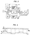
- Fig. 3 illustrates in block form an embodiment of the present invention, in which the parts corresponding to those in Fig. 1 are identified by the same reference numerals.
- the present invention employs offset generating means 21, which comprises, for instance, offset value generating means 22 for generating an offset voltage value and a DA converter 23 for converting the offset voltage value into an analog voltage.
- the offset voltage O from the offset generating means 21 is applied to the analog adder 12 in addition to the application of the noise signal N.
- the offset voltage O is varied more greatly than the quantization step size ⁇ ; namely, it is varied to, for example, +4 ⁇ , O, -4 ⁇ , O, +4 ⁇ , ..., as shown in Fig. 4.
- the variation period To of the offset voltage O is set to, for instance, m times longer than the sampling period Ts in the AD converter 15.
- the period To need not necessarily be held constant and synchronized with the sampling period Ts.
- the AD converter 15 provides a digital output (X + N + O) Q converted from the analog adder output (X + N + O).
- the digital value (O) Q of the offset voltage O is also subtracted, by the digital subtractor 16, from the output digital signal (X + N + O) Q of the AD converter 15, providing a digital signal (X + N + O) Q -(N + O) Q at the output terminal 17.
- the signal thus obtained at the output terminal 17 of the AD converting device is supplied to, for example, a digital fast Fourier transform unit 24, wherein the signal in the time domain is converted to a signal in the frequency domain, for analysis.
- the analog signal X to be converted into digital form is a repetitive signal
- the above-mentioned conversion to the frequency domain is conducted upon each repetition of the input signal X and the corresponding frequency components in the respective conversion results are averaged; this also averages quantization errors.
- Fig. 5 illustrates another embodiment of the present invention.
- respective values (sample values) of a random noise waveform are prestored in a random noise waveform memory 25, clock pulses of a frequency Ts from a clock terminal 26 are counted by a ring counter 27, and its count value is used as an address for reading out the memory 25.
- Each sample value of the random noise waveform read out of the memory 25 is latched in a latch circuit 28, the output of which is converted by the DA converter 14 to an analog signal. Consequently, an analog random noise is obtained from the DA converter 14.
- each sample value of an offset waveform is prestored in an offset waveform memory 29, the clock pulses from the terminal 26 are frequency divided by a frequency divider 31 down to 1/m of the clock pulses, and the frequency-divided outputs are counted by a ring counter 32.
- the count value of the ring counter 32 is used as an address for reading out the offset waveform memory 29.
- the sample values of the offset waveform thus read out of the memory 29 are latched in a latch circuit 33 by the output of the frequency divider 31.
- the latch output is converted by the DA converter 23 to analog form, in consequence of which analog offset voltage is obtained from the DA converter 23.
- the AD converter 15 performs one converting operation upon each application thereto of the clock pulse from the terminal 26.
- the digital subtractor 16 is supplied with the outputs from the latch circuits 28 and 33. In the embodiment of Fig. 5, it is necessary, in practice, to provide delay circuits for timing the operations of the respective parts, but no description will be given thereof for the sake of brevity.
- Fig. 6 shows a modified form of the embodiement of Fig. 5, in which the random noise and the offset voltage are generated by a common means.
- respective sample values of the random noise waveform and the offset waveform superimposed on each other are prestored in a waveform memory 34, which is read out using the count value of the counter 27, and the read-out output is latched in the latch circuit 28, the output of which is supplied to the DA converter 14.
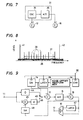
- Fig. 7 illustrates a modification of the offset generating means 21, in which an analog offset voltage is produced directly by a square-wave oscillator 35 and is applied not only to the analog adder 12 but also to an AD converter 36,wherein it is converted to a digital signal for input to the digital subtractor 16.
- the output digital signal at the output terminal 17 is converted to a signal of the frequency domain through use of, for example, the FFT unit 24 in Fig. 3.
- the frequency region (band) for observation is such as indicated by the broken line 37 in Fig. 8
- the frequency spectrum of the analog random noise N is substantially flat in at least the observation region, as indicated by 38, and the noise occurs at random.
- the frequency spectrum 38 of the analog random noise N is sufficiently lower in level than signal components 39 to be observed, as shown, it is not obstructive to the observation of the signal components 39.
- the digital subtractor 16 can be dispensed with in these cases. If the levels of the signal components 39 are sufficiently higher than the level of the offset volotage component 41 or 42, the digital subtractor 16 can be omitted also in the case of reproducing the AD converted output at the terminal 17 into an audio signal.
- the output of the divider 44 is provided via a changeover switch 46 to the analog adder 12.
- This is an example of application to the embodiment depicted in Fig. 6, in which the waveform memory 34 is read out, the read out output is converted to an analog signal to create a superimposed voltage of the random noise and the offset voltage, and the superimposed voltage is supplied to the analog adder 12.
- the output of the analog adder 12 is converted by the AD converter 15 to a digital signal, from which the random noise and the offset component are subtracted by the digital subtractor 16.
- a component of the digital subtractor output corresponding to the high-level portion of the input analog signal in terms of digital value has been shifted to a low level and then converted to a digital signal, which is latched in a latch circuit 47 and, at the same time, it is converted by a DA converter 48 to an analog signal.
- the level of the analog signal is returned to the original analog level, and the output of the DA converter 48 is applied to the analog subtractor 45, wherein the high-level portion of the original input analog signal at the input terminal 11 is subtracted by the DA converter output.
- the level of the remaining low-level portion from the analog subtractor 45 is raised by a multiplier 49, the output of which is provided via the switch 46 to the analog adder 12.
- the dividing number of the divider 44 and the multiplying number of the multiplier 49 are selected such that the full range of the AD converter 15 is utilized most effectively.
- the output of the multiplier 49 is also applied via the analog adder 12 to the AD converter 15 for conversion into a digital signal.
- the digital subtractor 16 the noise component and the offset component are removed from the converted output, and the subtractor output is supplied to an adder 51, wherein it is combined with the high-level portion previously converted and held in the latch circuit 47, into a composite signal, which is provided to the output terminal 17.
- the present inventor conducted the following experiment. As shown in Fig. 10, the output side of an analog subtractor 53 was connected to the input terminal 11 of the AD converting device, and the analog subtractor 53 was connected at one input to the output of a square wave generator 54 and at the other input to the output of a sine wave oscillator 55 via a switch 56. A sine wave of the same frequency and amplitude as those of the fundamental wave of the output square wave of the square wave generator 54 was produced by the sine wave oscillator 55. Incidentally, the digital subtractor 16 was left out.
- the switch 56 was turned ON and the outputs of the both DA converters 13 and 23 were set to zero. Consequently, the fundamental wave component of the output from the square wave generator 54 was cancelled by the sine wave from the oscillator 55 and only high-frequency components of the square wave were provided via the analog adder 12 to the AD converter 15.
- the AD converted output was transformed by the means 24 into a signal of the frequency domain, and the level of each high-frequency component was regarded as a true value.
- the switch 56 was turned OFF, the output of the DA converter 23 was held at zero, and the output of the square wave generator 54 was supplied to the analog adder 12 so as to measure, first, the quantization error according to the prior art device.
- the output of the DA converter 14 was provided to the analog adder 12, and the amplitude of the output of the DA converter 14, that is, the amplitude of the analog random noise was gradually increased, and then the quantization error of the converted output by the AD converter 15 was measured.
- the measured results are shown in Fig. 2 as referred to previously.
- the quantization error is defined as the sum of the differences between the frequency components of the output from the means 24 and the afore-said true values.
- the amplitude of the output from the DA converter 14, that is, the amplitude of the analog offset voltage was gradually increased, starting with zero, while maintaining the amplitude of random noise at 2 ⁇ where the quantization error was minimum as seen in Fig. 2.
- the measured results of the quantization error with respect to the increase in the offset voltage are such as shown in Fig. 11.
- an increase in the amplitude of the offset voltage causes a decrease in the quantization error, and when the alternating amplitude of the offset voltage is ⁇ 4 ⁇ about zero, the quantization error is minimum.
- the amplitude variations in the range of ⁇ ( ⁇ to 7 ⁇ ) are also effective compared to Fig. 2 for reducing the quantization error and variations in the range of ⁇ (3 to 6 ⁇ ) are also appreciably effective.
- the amplitude of a random noise superimposed on an analog signal to be converted can be decreased even by superimposing on the latter an offset voltage of alternating levels; so that the digital subtractor 16 need not always be provided at the output side of the AD converter 15, as mentioned previously.
- a DA converter which is small in the number of bits, small-sized, low-cost, excellent in linearity and high in precision. This ensures correct compensation for cancellation by the digital subtractor 16 if employed.
- the use of the offset voltage not only permits uniform distribution of the quantization error but also suppresses the influences of variations in the quantization step size and the nonlinearity of conversion characteristics of the AD converter.
- a DA converter with a small number of bits can be used as the DA converter 23 for generating the offset voltage, too. Moreover, since the quantization error is reduced through utilization of both the random noise and the offset voltage, a suitable selection of their amplitudes provides for increased freedom in designing the AD converting device.
Landscapes
- Engineering & Computer Science (AREA)
- Theoretical Computer Science (AREA)
- Analogue/Digital Conversion (AREA)
Description
- The present invention relates to an AD converting device which is employed for converting an audio signal, musical signal, image signal, or like analog signal into a digital signal which may be subjected to, for instance, an analysis in the frequency domain and/or time domain.
- A quantization error is incidental to an AD conversion because an AD converter has a limited number of quantization steps. Many attempts have been made to average maldistributed quantization errors through application of a dither to an original analog signal by using a random noise, as set forth in, for example, B. A. Blesser, "Digitization of Audio: A Comprehensive Examination of Theory, Implementation, and Current Practice", Journal of Audio Enginnering Society, Oct. 1978, Vol. 26, No. 10.
- Fig. 1 shows a prior art example. An analog signal X for conversion into a digital signal is applied to an
analog adder 12 from aninput terminal 11. Arandom pulse generator 13 is provided, which is an M-sequence pulse generator comprising a shift register. Random pulses generated in digital form by therandom pulse generator 13 are converted by aDA converter 14 into an analog random noise signal N. which is supplied to theanalog adder 12 for addition to the analog signal X. The adder output (X + N) is provided to anAD converter 15, whereby it is converted, at intervals of a fixed period Ts, into a digital signal of a predetermined number of bits. - The converted output (X + N)Q (where Q indicates that the output is a digital signal) from the
AD converter 15 is applied, as required, to adigital subtractor 16, wherein a random noise value (N)Q supplied from therandom pulse generator 13 is digitally subtracted from the converted output (X + N)Q, providing an output (X + N)Q -(N)Q at anoutput terminal 17. - In the conventional AD converting device of the type that superimposes the random noise on the analog signal to be converted, it is possible to distribute quantization errors uniformly over the quantization step size Δ when the amplitude of the random noise N is selected to exceed about one-half the quantization step size Δ of the
AD converter 15. An increased amplitude of the random noise N will also lessen the influences of the nonlinearity of the quantization characteristic of theAD converter 15 and variations in its quantization step size owing to averaging effects. From this point of view, the random noise N may preferably be large in amplitude. - In the case where the random noise N has a small amplitude but the analog signal to be converted has a large amplitude, small noises will be masked by the signal if it is reproduced into an audio signal. Therefore, the
digital subtractor 16 in Fig. 1 can be left out. Furthermore, when the output at theoutput terminal 17 is subjected to a digital fast Fourier transform (FFT) or digital discrete Fourier transform (DFT) for a frequency analysis, if the random noise N is small, the resultant signal component appearing on the observation screen may have high peaks above the low random noise levels distributed in the analyzing frequency range; and so the random noise is not obstructive to the observation of the signal component. Accordingly, thedigital subtractor 16 can be dispensed with in this case, too. - On the other hand, when the amplitude of the random noise is increased as mentioned above, the noise component is distrubuted uniformly over a wide frequency band with high levels; therefore, it is necessary to remove the random noise component by means of the
digital subtractor 16. - Moreover, according to the above prior art system, the random pulses from the
random pulse generator 13 are converted by thePA converter 14 into an analog signal. In this case, if the amplitude of the random pulses (noise) is large, the nonlinearlity of theDA converter 14 cannot be ignored in the DA conversion and there arises the necessity of employing an expensive DA converter of a large dynamic range of conversion. Thus, the nonlinearity of theDA converter 14 prevents complete elimination of the random noise in spite of its subtraction by thedigital subtractor 16. - Incidentally, there are shown in Fig. 2 variations in a quantization error produced when the amplitude of the random noise N was varied in the conventional AD converting device depicted in Fig. 1. The random noise amplitude on the horizontal axis in Fig. 2 is expressed in normalized form with the quantization step size Δ . As will be seen from Fig. 2, an increase in the amplitude of the random noise N causes a decrease in the quantization error, but in this example, the error reaches a minimum value at a noise amplitude of 2Δ and thereafter it is rather on the increase.
- An AD converting device according to the precharacterizing portion of
claim 1 is disclosed in document EP O 037 259. In this prior art, the analog offset voltage is a square wave voltage synchronized with the sampling signal and having a frequency half that of the sampling frequency. This document discloses that where the amplitude of the offset voltage is selected such that the difference between adjacent sampled values resulting from adjacent samplings is (2n+1)QS/2 with n = 0,1,2,2,... and QS the quantum step, the quantization distortion reduction effect becomes most remarkable. The document further mentions that the analog offset voltage may be used with or without analog random noise being added to the analog signal to be converted. Where analog random noise is added, the level of the noise signal is required to be only one half the level that is conventionally used, thus reducing a deterioration of the S/N ratio. - An AD converting device disclosed in US-A-3,877,022 is concerned with a solution of the problem to enhance the resolution of the AD converting device without unduly complicating it. In particular, the noise signal that is combined with the analog input signal prior to conversion is chosen to have a power spectrum which is outside the power spectrum of the analog input signal and of the sampling signal used in conversion, and the noise signal has a defined amplitude probability density in that selected power spectrum. To that end the document teaches that the noise signal should ideally have an amplitude probability density function which is zero except over the interval between one-half of a quantization step below the analog input signal and one-half of a quantization step above the analog input signal. Over the interval where it is not zero, the amplitude probability density function of the noise signal should have a specified constant value. The effect of this prior art is the same as that of the prior art explained with respect to Fig. 1.
- The document ELECTRONICS INTERNATIONAL, Vol.53, No.20, 11th September 1989, pages 171-172, New York, US; L.M. LOWE: "8-bit a-d converter has 12-bit linearity", discloses an 8-bit AD converter which is said to have a 12-bit linearity. This is accomplished by scattering linearity errors over the AD converter's own full-scale range. Thus randomized, the errors average out over a large number of samples, just as noise does, to leave a high-quality signal. This prior art corresponds to that described with respect to Fig. 1.
- It is therefore an object of the present invention to provide an AD converting device which is relatively simple-structured and low-cost and is able not only to reduce the maldistribution of a quantization error but also to lessen the influences of variations in quantization steps and the nonlinearity of conversion characteristics of the AD converter used.
- Another object of the present invention is to provide an AD converting device which dispenses with a digital subtraction of the random noise from the AD converter output.
- Yet another object of the present invention is to provide an AD converting device which is capable of lessening the influences of non-uniformity of quantization steps and the nonlinearity of conversion characteristics of the AD converter even if a random noise of a relatively small amplitude is employed.
- These objects are achieved with an AD converting device as claimed in
claim 1. - Specific embodiments of the invention are subject matter of the dependent claims.
- The alternation level of the analog offset voltage is selected larger than the amplitude of the random noise, in general, about one to seven times the quantization step size Δ of the AD converter, preferably three to six times, in particular, around four times the quantization step size. The period of variation of the analog offset voltage needs only to satisfy the condition that its frequency spectrum stays outside the frequency band (i.e. the observation frequency region) of the object signal. When the analog offset voltage takes the form of a square wave: its period of variation is selected to be at least four times longer than the conversion period of so-called sampling period Ts of the AD converter, for instance, 256 Ts, and its variation need not be synchronized with sampling by the AD converter.
- The amplitude of the analog random noise is set to 6Δ or less, preferably in the range of Δ/2 to 4Δ or so. With a noise amplitude exceeding 10Δ, the nonlinearity of the DA converter for converting the digital random noise into an analog noise poses a problem and a costly DA converter is required in prior art system.
- As described above, according to the present invention, since the analog offset voltage is superimposed on the analog signal to be converted, the influence of nonuniformity of the quantization steps and the non-linearity of the conversion characteristics on the AD conversion can be lessened even if the amplitude of the analog random noise is reduced. In addition, since the spectrum of the analog offset voltage is placed outside the observation frequency range and the amplitude of the analog random noise is small, neither the offset voltage nor the random noise needs to be subtracted digitally from the AD converter output. Of course, the subtraction may also be conducted. Further, a low-cost PA converter with a small number of bits can be employed for producing the analog random noise because its amplitude is small, and a DA converter of excellent conversion linearity is easily available.
- Moreover, since the amplitude of the random noise and the level alternation (amplitude) of the offset voltage can be selected in various combinations, the freedom in designing the AD converting device is increased accordingly.
-
- Fig. 1 is a block diagram illustrating a conventional AD converting device;
- Fig. 2 is a graph showing the relation between the amplitude of a random noise and a quantization error in the AD converting device depicted in Fig. 1;
- Fig. 3 is a block diagram illustrating an embodiment of the AD converting device of the present invention;
- Fig. 4 is a timing chart showing an example of the relation between a sampling clock and an offset voltage;
- Fig. 5 is a block diagram illustrating another embodiment of the AD converting device which employs waveform memories for generating the random noise and the offset voltage;
- Fig. 6 is a block diagram illustrating another embodiment of the present invention which employs a common waveform memory for producing the random noise and the offset voltage;
- Fig. 7 is a block diagram illustrating another example of the offset voltage generating means;
- Fig. 8 is a frequency spectrum showing, by way of example, the relations between observation band, a signal to be observed, noise, and the offset voltage component;
- Fig. 9 is a block diagram illustrating an example of the present invention as applied to the case of converting an analog signal into a digital signal in two stages;
- Fig. 10 is a block diagram illustrating an example of a measuring system, for explaining the effect of the present invention; and
- Fig. 11 is a graph showing an experimental example of the relation between the amplitude (level variation) of the offset voltage and a quantization error.
- Fig. 3 illustrates in block form an embodiment of the present invention, in which the parts corresponding to those in Fig. 1 are identified by the same reference numerals. The present invention employs offset generating means 21, which comprises, for instance, offset value generating means 22 for generating an offset voltage value and a
DA converter 23 for converting the offset voltage value into an analog voltage. The offset voltage O from the offset generating means 21 is applied to theanalog adder 12 in addition to the application of the noise signal N. The offset voltage O is varied more greatly than the quantization step size Δ; namely, it is varied to, for example, +4Δ, O, -4Δ, O, +4Δ, ..., as shown in Fig. 4. In this case, however, the values of these variations need not always be integral multiples of the quantization step size Δ. The variation period To of the offset voltage O is set to, for instance, m times longer than the sampling period Ts in theAD converter 15. The period To need not necessarily be held constant and synchronized with the sampling period Ts. - The
AD converter 15 provides a digital output (X + N + O)Q converted from the analog adder output (X + N + O). In this example, the digital value (O)Q of the offset voltage O is also subtracted, by thedigital subtractor 16, from the output digital signal (X + N + O)Q of theAD converter 15, providing a digital signal (X + N + O)Q -(N + O)Q at theoutput terminal 17. - The signal thus obtained at the
output terminal 17 of the AD converting device is supplied to, for example, a digital fastFourier transform unit 24, wherein the signal in the time domain is converted to a signal in the frequency domain, for analysis. Where the analog signal X to be converted into digital form is a repetitive signal, the above-mentioned conversion to the frequency domain is conducted upon each repetition of the input signal X and the corresponding frequency components in the respective conversion results are averaged; this also averages quantization errors. - Fig. 5 illustrates another embodiment of the present invention. In this embodiment, respective values (sample values) of a random noise waveform are prestored in a random
noise waveform memory 25, clock pulses of a frequency Ts from aclock terminal 26 are counted by aring counter 27, and its count value is used as an address for reading out thememory 25. Each sample value of the random noise waveform read out of thememory 25 is latched in alatch circuit 28, the output of which is converted by theDA converter 14 to an analog signal. Consequently, an analog random noise is obtained from theDA converter 14. - On the other hand, each sample value of an offset waveform is prestored in an offset
waveform memory 29, the clock pulses from the terminal 26 are frequency divided by afrequency divider 31 down to 1/m of the clock pulses, and the frequency-divided outputs are counted by aring counter 32. The count value of thering counter 32 is used as an address for reading out the offsetwaveform memory 29. The sample values of the offset waveform thus read out of thememory 29 are latched in alatch circuit 33 by the output of thefrequency divider 31. The latch output is converted by theDA converter 23 to analog form, in consequence of which analog offset voltage is obtained from theDA converter 23. - The
AD converter 15 performs one converting operation upon each application thereto of the clock pulse from the terminal 26. Thedigital subtractor 16 is supplied with the outputs from thelatch circuits - Fig. 6 shows a modified form of the embodiement of Fig. 5, in which the random noise and the offset voltage are generated by a common means. In this instance, respective sample values of the random noise waveform and the offset waveform superimposed on each other are prestored in a
waveform memory 34, which is read out using the count value of thecounter 27, and the read-out output is latched in thelatch circuit 28, the output of which is supplied to theDA converter 14. - Fig. 7 illustrates a modification of the offset generating means 21, in which an analog offset voltage is produced directly by a square-
wave oscillator 35 and is applied not only to theanalog adder 12 but also to anAD converter 36,wherein it is converted to a digital signal for input to thedigital subtractor 16. - Let the case be considered that the output digital signal at the
output terminal 17 is converted to a signal of the frequency domain through use of, for example, theFFT unit 24 in Fig. 3. When the frequency region (band) for observation is such as indicated by thebroken line 37 in Fig. 8, the frequency spectrum of the analog random noise N is substantially flat in at least the observation region, as indicated by 38, and the noise occurs at random. Where thefrequency spectrum 38 of the analog random noise N is sufficiently lower in level thansignal components 39 to be observed, as shown, it is not obstructive to the observation of thesignal components 39. When thesignal components 39 are reproduced into an audio signal, it hears that the noise is almost masked by the highintensity signal components 39; and so there may be no need of the subtraction of the digital random noise (N)Q by thedigital subtractor 16 in the above-described embodiments. Similarly, by suitably selecting the offset voltage such that the frequency component of the offset voltage falls outside theobservation band 37, as indicated by 41 or 42 in Fig. 8, the offset component need not be subtracted by thedigital subtractor 16 either. Accordingly, thedigital subtractor 16 can be dispensed with in these cases. If the levels of thesignal components 39 are sufficiently higher than the level of the offsetvolotage component digital subtractor 16 can be omitted also in the case of reproducing the AD converted output at the terminal 17 into an audio signal. - It has been proposed to employ a relatively small, high-performance, high-speed AD converter for an AD conversion, in which an analog signal to be converted to digital form is figuratively divided into a high-level portion and a low-level portion in terms of digital value, the both portions are shifted into substantially the same level range and individually converted to digital signals, and then the digital signals are combined into a composite signal after being adjusted in order. This is introduced in, for instance, HEWLETT PACKARD JOURNAL, Dec. 1984, pp. 13-15. Also in such an instance the present invention can be utilized. For example, as shown in Fig. 9, the analog signal from the
input terminal 11 is supplied to both ananalog divider 44 and ananalog subtractor 45. The output of thedivider 44 is provided via achangeover switch 46 to theanalog adder 12. This is an example of application to the embodiment depicted in Fig. 6, in which thewaveform memory 34 is read out, the read out output is converted to an analog signal to create a superimposed voltage of the random noise and the offset voltage, and the superimposed voltage is supplied to theanalog adder 12. The output of theanalog adder 12 is converted by theAD converter 15 to a digital signal, from which the random noise and the offset component are subtracted by thedigital subtractor 16. As a result of this, a component of the digital subtractor output corresponding to the high-level portion of the input analog signal in terms of digital value has been shifted to a low level and then converted to a digital signal, which is latched in alatch circuit 47 and, at the same time, it is converted by aDA converter 48 to an analog signal. At this time, the level of the analog signal is returned to the original analog level, and the output of theDA converter 48 is applied to theanalog subtractor 45, wherein the high-level portion of the original input analog signal at theinput terminal 11 is subtracted by the DA converter output. The level of the remaining low-level portion from theanalog subtractor 45 is raised by amultiplier 49, the output of which is provided via theswitch 46 to theanalog adder 12. - In this arrangement, the dividing number of the
divider 44 and the multiplying number of themultiplier 49 are selected such that the full range of theAD converter 15 is utilized most effectively. As described above, the output of themultiplier 49 is also applied via theanalog adder 12 to theAD converter 15 for conversion into a digital signal. In thedigital subtractor 16 the noise component and the offset component are removed from the converted output, and the subtractor output is supplied to anadder 51, wherein it is combined with the high-level portion previously converted and held in thelatch circuit 47, into a composite signal, which is provided to theoutput terminal 17. - In order to varify the effect of the present invention, the present inventor conducted the following experiment. As shown in Fig. 10, the output side of an
analog subtractor 53 was connected to theinput terminal 11 of the AD converting device, and theanalog subtractor 53 was connected at one input to the output of asquare wave generator 54 and at the other input to the output of asine wave oscillator 55 via aswitch 56. A sine wave of the same frequency and amplitude as those of the fundamental wave of the output square wave of thesquare wave generator 54 was produced by thesine wave oscillator 55. Incidentally, thedigital subtractor 16 was left out. - At first, the
switch 56 was turned ON and the outputs of the bothDA converters square wave generator 54 was cancelled by the sine wave from theoscillator 55 and only high-frequency components of the square wave were provided via theanalog adder 12 to theAD converter 15. The AD converted output was transformed by themeans 24 into a signal of the frequency domain, and the level of each high-frequency component was regarded as a true value. - After this, the
switch 56 was turned OFF, the output of theDA converter 23 was held at zero, and the output of thesquare wave generator 54 was supplied to theanalog adder 12 so as to measure, first, the quantization error according to the prior art device. At that time, the output of theDA converter 14 was provided to theanalog adder 12, and the amplitude of the output of theDA converter 14, that is, the amplitude of the analog random noise was gradually increased, and then the quantization error of the converted output by theAD converter 15 was measured. The measured results are shown in Fig. 2 as referred to previously. The quantization error is defined as the sum of the differences between the frequency components of the output from themeans 24 and the afore-said true values. - Next, the amplitude of the output from the
DA converter 14, that is, the amplitude of the analog offset voltage was gradually increased, starting with zero, while maintaining the amplitude of random noise at 2Δ where the quantization error was minimum as seen in Fig. 2. The measured results of the quantization error with respect to the increase in the offset voltage are such as shown in Fig. 11. As is evident from Fig. 11, an increase in the amplitude of the offset voltage causes a decrease in the quantization error, and when the alternating amplitude of the offset voltage is ±4Δ about zero, the quantization error is minimum. Further, it is seen from Fig. 11 that the amplitude variations in the range of ±(Δ to 7Δ) are also effective compared to Fig. 2 for reducing the quantization error and variations in the range of ±(3 to 6Δ) are also appreciably effective. - As described above, according to the present invention, the amplitude of a random noise superimposed on an analog signal to be converted can be decreased even by superimposing on the latter an offset voltage of alternating levels; so that the
digital subtractor 16 need not always be provided at the output side of theAD converter 15, as mentioned previously. Furthermore, it is possible to employ, for producing the random noise voltage, a DA converter which is small in the number of bits, small-sized, low-cost, excellent in linearity and high in precision. This ensures correct compensation for cancellation by thedigital subtractor 16 if employed. In addition, the use of the offset voltage not only permits uniform distribution of the quantization error but also suppresses the influences of variations in the quantization step size and the nonlinearity of conversion characteristics of the AD converter. - A DA converter with a small number of bits can be used as the
DA converter 23 for generating the offset voltage, too. Moreover, since the quantization error is reduced through utilization of both the random noise and the offset voltage, a suitable selection of their amplitudes provides for increased freedom in designing the AD converting device.
Claims (14)
- An AD converting device in which an analog random noise is generated by random noise generating means (13,14; 14,25,27; 14,27,34), an analog offset voltage having alternating levels is generated by offset generating means (21; 14,27,34), the analog random noise and the analog offset voltage are added by analog adding means (12) to an analog signal to be converted, and the added output is converted by an AD converter (15) to a digital signal, wherein the variation between successive alternating levels of said offset voltage is greater than the quantization step of the AD converter (15), characterized in that
said analog random noise is equal to or greater in level than half the quantization step of said AD converter (15), and the period between successive alternations of the level of said offset voltage is four times or more the sampling period. - The AD converting device according to claim 1, wherein the random noise generating means comprises digital random noise generating means (13) for generating a digital random noise and first DA converting means (14) for converting the digital random noise into the analog random noise to be applied to the analog adding means.
- The AD converting device according to claim 2, wherein the digital random noise generating means includes first memory means (25) for storing a digital random noise waveform, the output read out of the first memory means being supplied as the digital random noise to the first DA converting means (14).
- The AD converting device according to claim 3, wherein the offset voltage generating means (21) comprises second memory means (19) for storing a digital offset waveform, and second DA converting means (23) for converting the digital offset waveform into the analog offset voltage.
- The AD converting device according to claim 4, wherein one DA converting means (14) is used both as the first DA converting means and as the second DA converting means and one memory means (34) is used both as the first memory means and as the second memory means, and wherein the digital random noise waveform and the digital offset waveform superimposed on each other are stored in the memory means (34) which are repeatedly read out therefrom, converted by the DA converting means (14) to analog form, and then applied to the analog adding means (12).
- The AD converting device according to claim 4, further including means (27) for repeatedly reading out the first memory means (25) in synchronization with first clock pulses of a conversion period of the AD converter (15) and means (23) for repeatedly reading out the second memory means (29) by second clock pulses lower in rate than the first clock pulses.
- The AD converting device according to claim 1, wherein the offset voltage generating means (21) comprises memory means (29) for storing a digital offset waveform and DA converting means (23) for converting the digital offset waveform to the analog offset voltage.
- The AD converting device according to claim 1, wherein the offset generating means (21) includes an offset generator (35) which directly generates the analog offset voltage, characterized in the provision of AD converting means (36) for converting the analog offset voltage from the offset generator into a digital offset signal and digital subtracting means (16) for subtracting the converted digital offset signal from the output of the AD converter (15).
- The AD converting device according to any one of claims 4 to 7, further including digital subtracting means (16) for subtracting from the output of the AD converter (15) the digital offset waveform read out of the memory means (29).
- The AD converting device according to claim 9, wherein the digital subtracting means (16) performs the subtraction of the digital noise waveform from the output of the AD converter as well.
- The AD converting device according to claim 10, comprising:
analog dividing means (44) for dividing the level of the input analog signal by a given value; third DA converting means (48) for converting the output of the digital subtracting means (16) into an analog level; analog subtracting means (45) for subtracting the output of the third DA converting means (48) from the input analog signal; switch means (46) selectively supplying the outputs of the analog dividing means (44) and the analog subtracting means (45) to the analog adding means (12); and combining means (47, 51) for combining the outputs of the digital subtracting means (16) respectively obtainable when the output of the analog dividing means is supplied to the analog adding means and when the output of the analog subtracting means is supplied to the analog adding means, the combined outputs being the output of the AD converting device. - The AD converting device according to any one of claims 1 and 3 to 7, wherein the amplitude of the analog random noise is selected about 6 or less times the quantization step size Δ of the AD converter (15).
- The AD converting device according to claim 12, wherein the level variation of the analog offset voltage is about 7 or less times the quantization step size Δ of the AD converter (15).
- The AD converting device according to any one of claims 1 and 3 to 8, wherein the level variation of the analog offset voltage is about 7 or less times the quantization step size Δ of the AD converter (15).
Applications Claiming Priority (2)
| Application Number | Priority Date | Filing Date | Title |
|---|---|---|---|
| JP60280652A JPS62140518A (en) | 1985-12-13 | 1985-12-13 | A/d converter |
| JP280652/85 | 1985-12-13 |
Publications (3)
| Publication Number | Publication Date |
|---|---|
| EP0225641A2 EP0225641A2 (en) | 1987-06-16 |
| EP0225641A3 EP0225641A3 (en) | 1988-12-07 |
| EP0225641B1 true EP0225641B1 (en) | 1993-04-14 |
Family
ID=17628039
Family Applications (1)
| Application Number | Title | Priority Date | Filing Date |
|---|---|---|---|
| EP86117203A Expired - Lifetime EP0225641B1 (en) | 1985-12-13 | 1986-12-10 | Ad converting device |
Country Status (4)
| Country | Link |
|---|---|
| US (1) | US4761634A (en) |
| EP (1) | EP0225641B1 (en) |
| JP (1) | JPS62140518A (en) |
| DE (1) | DE3688279T2 (en) |
Families Citing this family (30)
| Publication number | Priority date | Publication date | Assignee | Title |
|---|---|---|---|---|
| JPS63244486A (en) * | 1987-03-31 | 1988-10-11 | Toshiba Corp | Semiconductor device |
| JP2573850B2 (en) * | 1987-09-14 | 1997-01-22 | ティアツク株式会社 | Analog-to-digital converter |
| US5010347A (en) * | 1987-09-25 | 1991-04-23 | Nec Corporation | Analog-to-digital converter having an excellent signal-to-noise ratio for small signals |
| JP2575754B2 (en) * | 1987-11-20 | 1997-01-29 | 株式会社アドバンテスト | Frequency response function measurement method |
| JPH0228713A (en) * | 1988-04-26 | 1990-01-30 | Mitsubishi Electric Corp | Device and method for acquiring signal |
| AU623462B2 (en) * | 1989-02-03 | 1992-05-14 | Alcatel Australia Limited | Digital converter |
| JP3012887B2 (en) * | 1989-03-13 | 2000-02-28 | 日本テキサス・インスツルメンツ株式会社 | Signal converter |
| JPH02301327A (en) * | 1989-05-16 | 1990-12-13 | Pioneer Electron Corp | Digital/analog conversion circuit |
| US5144308A (en) * | 1991-05-21 | 1992-09-01 | At&T Bell Laboratories | Idle channel tone and periodic noise suppression for sigma-delta modulators using high-level dither |
| US5113189A (en) * | 1991-06-21 | 1992-05-12 | Motorola, Inc. | Frequency translating coherent analog to digital conversion system for modulated signals |
| US5250948A (en) * | 1991-12-19 | 1993-10-05 | Eastman Kodak Company | High level resolution enhancement for dual-range A/D conversion |
| JPH0554077U (en) * | 1991-12-20 | 1993-07-20 | 宮島 泰重 | Drink holder |
| US5189418A (en) * | 1992-04-16 | 1993-02-23 | Hewlett-Packard Company | Dither error correction |
| DE69325679T2 (en) * | 1992-04-30 | 1999-11-11 | Hewlett Packard Co | Analog / digital converter with automatic offset range control |
| US5351084A (en) * | 1992-07-02 | 1994-09-27 | Global Telecommunications Industries, Inc. | Compressed video bit rate reduction system |
| US5406495A (en) * | 1993-02-01 | 1995-04-11 | Systems Analysis And Integration, Inc. | Substation load distribution monitor system |
| DE69322762T2 (en) * | 1993-02-26 | 1999-06-02 | Schlumberger Industries S.A., Montrouge | AD converter with modulated dither signal |
| US5629703A (en) * | 1995-08-09 | 1997-05-13 | Tektronix, Inc. | Method for reducing harmonic distortion in an analog-to-digital converter system |
| DE19720548C2 (en) * | 1997-05-16 | 2003-07-10 | Rohde & Schwarz | Analog / digital converter |
| SE509408C2 (en) * | 1997-05-27 | 1999-01-25 | Ericsson Telefon Ab L M | Apparatus and method for reducing periodic noise in a sigma-delta modulator |
| US6028543A (en) * | 1997-10-03 | 2000-02-22 | Eg&G Instruments, Inc. | Apparatus for improvement of the speed of convergence to sub-least-significant-bit accuracy and precision in a digital signal averager and method of use |
| US6433723B1 (en) | 1998-07-30 | 2002-08-13 | Siemens Power Transmission & Distribution, Inc. | Analog-to-digital conversion with reduced error |
| FR2783374B1 (en) | 1998-09-11 | 2000-12-08 | Thomson Csf | METHOD AND DEVICE FOR GENERATING A RANDOM SIGNAL AND DIGITAL-ANALOG CONVERSION SYSTEMS USING SUCH A RANDOM SIGNAL |
| US6469792B1 (en) * | 2000-03-01 | 2002-10-22 | Raytheon Company | Method for processing the output of a fiber optic gyroscope to reduce the effects of vibration therefrom |
| US7315277B2 (en) * | 2002-04-30 | 2008-01-01 | The Johns Hopkins University | Bit depth reduction for analog to digital conversion in global positioning system |
| DE102004025577B4 (en) * | 2004-05-25 | 2010-05-06 | Infineon Technologies Ag | Suppression of even harmonic distortions in a non-linear element |
| JP3971414B2 (en) * | 2004-07-16 | 2007-09-05 | ローム株式会社 | A / D conversion device and communication device using the same |
| WO2007038280A1 (en) * | 2005-09-23 | 2007-04-05 | University Of Rochester | Blue-noise-modulated sigma-delta analog-to-digital converter |
| US8174418B2 (en) | 2009-07-14 | 2012-05-08 | Honeywell International Inc. | Inexpensively improving resolution and reducing noise of low-noise signals |
| US10193585B2 (en) * | 2017-02-17 | 2019-01-29 | SiTune Corporation | Tone removal for digital circuits |
Family Cites Families (6)
| Publication number | Priority date | Publication date | Assignee | Title |
|---|---|---|---|---|
| US2669608A (en) * | 1950-10-27 | 1954-02-16 | Bell Telephone Labor Inc | Noise reduction in quantized pulse transmission systems with large quanta |
| US3877022A (en) * | 1973-05-14 | 1975-04-08 | Weston Instruments Inc | Enhancing resolution in analog-to-digital conversion by adding statistically controlled noise to the analog input signal |
| JPS5639576B2 (en) * | 1973-10-17 | 1981-09-14 | ||
| US4327419A (en) * | 1980-02-22 | 1982-04-27 | Kawai Musical Instrument Mfg. Co., Ltd. | Digital noise generator for electronic musical instruments |
| JPS56136027A (en) * | 1980-03-27 | 1981-10-23 | Victor Co Of Japan Ltd | Signal processor having quantization distortion reduced |
| US4550309A (en) * | 1984-02-16 | 1985-10-29 | Hewlett Packard Company | Analog to digital converter |
-
1985
- 1985-12-13 JP JP60280652A patent/JPS62140518A/en active Pending
-
1986
- 1986-12-10 EP EP86117203A patent/EP0225641B1/en not_active Expired - Lifetime
- 1986-12-10 US US06/940,058 patent/US4761634A/en not_active Expired - Fee Related
- 1986-12-10 DE DE86117203T patent/DE3688279T2/en not_active Expired - Fee Related
Also Published As
| Publication number | Publication date |
|---|---|
| JPS62140518A (en) | 1987-06-24 |
| DE3688279T2 (en) | 1993-11-18 |
| DE3688279D1 (en) | 1993-05-19 |
| EP0225641A3 (en) | 1988-12-07 |
| EP0225641A2 (en) | 1987-06-16 |
| US4761634A (en) | 1988-08-02 |
Similar Documents
| Publication | Publication Date | Title |
|---|---|---|
| US4761634A (en) | AD converting device | |
| EP0383689A2 (en) | Digital-to-analog converter | |
| US5138317A (en) | Digital to analogue converter adapted to select input sources based on a preselected algorithm once per cycle of a sampling signal | |
| JP2010045789A (en) | Analog-to-digital converter | |
| US5905453A (en) | Dithered sigma delta modulator having programmable full scale range adjustment | |
| CA2292615A1 (en) | Analogue-to-digital conversion using frequency-modulated input or intermediate values | |
| US5818372A (en) | D/A converter circuit having offset voltage application device | |
| US4864305A (en) | D/A converter | |
| US4937579A (en) | Method of converting analog signals into digital signals and system for carrying out the method | |
| EP0037259A1 (en) | Circuit arrangement and method for reducing quantization distortion in a signal processing device | |
| US4191921A (en) | Corona discharge detection apparatus which eliminates periodic noise | |
| US4758781A (en) | DA converter testing system | |
| US4654634A (en) | Apparatus for processing a sequence of digital data values | |
| JPH08293793A (en) | Circuit for A / D conversion of video radio frequency or intermediate frequency signal | |
| JP3144563B2 (en) | Waveform measuring device | |
| US5760617A (en) | Voltage-to-frequency converter | |
| US4916449A (en) | Wide dynamic range digital to analog conversion method and system | |
| JPS60107932A (en) | Analog-digital converter | |
| US5010339A (en) | Ultra linear spectroscopic analog-to-digital converter | |
| US4729011A (en) | Method and apparatus for digitizing television signals | |
| Carbone et al. | Mean value and variance of noisy quantized data | |
| JPS5821979B2 (en) | Image signal halftone processing method | |
| JP3061884B2 (en) | Analog-to-digital conversion system and spectral histogram generation method | |
| US5638073A (en) | Method of linearizing variations in the transfer characteristic of a D/A converter, as well as an arrangement and use thereof | |
| JPS60197016A (en) | Analog-digital converting circuit device |
Legal Events
| Date | Code | Title | Description |
|---|---|---|---|
| PUAI | Public reference made under article 153(3) epc to a published international application that has entered the european phase |
Free format text: ORIGINAL CODE: 0009012 |
|
| AK | Designated contracting states |
Kind code of ref document: A2 Designated state(s): DE GB NL |
|
| PUAL | Search report despatched |
Free format text: ORIGINAL CODE: 0009013 |
|
| AK | Designated contracting states |
Kind code of ref document: A3 Designated state(s): DE GB NL |
|
| 17P | Request for examination filed |
Effective date: 19890519 |
|
| 17Q | First examination report despatched |
Effective date: 19900926 |
|
| GRAA | (expected) grant |
Free format text: ORIGINAL CODE: 0009210 |
|
| AK | Designated contracting states |
Kind code of ref document: B1 Designated state(s): DE GB NL |
|
| REF | Corresponds to: |
Ref document number: 3688279 Country of ref document: DE Date of ref document: 19930519 |
|
| PGFP | Annual fee paid to national office [announced via postgrant information from national office to epo] |
Ref country code: GB Payment date: 19931130 Year of fee payment: 8 |
|
| PGFP | Annual fee paid to national office [announced via postgrant information from national office to epo] |
Ref country code: DE Payment date: 19931220 Year of fee payment: 8 |
|
| PGFP | Annual fee paid to national office [announced via postgrant information from national office to epo] |
Ref country code: NL Payment date: 19931231 Year of fee payment: 8 |
|
| PLBE | No opposition filed within time limit |
Free format text: ORIGINAL CODE: 0009261 |
|
| STAA | Information on the status of an ep patent application or granted ep patent |
Free format text: STATUS: NO OPPOSITION FILED WITHIN TIME LIMIT |
|
| 26N | No opposition filed | ||
| PG25 | Lapsed in a contracting state [announced via postgrant information from national office to epo] |
Ref country code: GB Effective date: 19941210 |
|
| PG25 | Lapsed in a contracting state [announced via postgrant information from national office to epo] |
Ref country code: NL Effective date: 19950701 |
|
| GBPC | Gb: european patent ceased through non-payment of renewal fee |
Effective date: 19941210 |
|
| NLV4 | Nl: lapsed or anulled due to non-payment of the annual fee |
Effective date: 19950701 |
|
| PG25 | Lapsed in a contracting state [announced via postgrant information from national office to epo] |
Ref country code: DE Effective date: 19950901 |