EP0217281B1 - Method of manufacturing an IC card - Google Patents
Method of manufacturing an IC card Download PDFInfo
- Publication number
- EP0217281B1 EP0217281B1 EP86113130A EP86113130A EP0217281B1 EP 0217281 B1 EP0217281 B1 EP 0217281B1 EP 86113130 A EP86113130 A EP 86113130A EP 86113130 A EP86113130 A EP 86113130A EP 0217281 B1 EP0217281 B1 EP 0217281B1
- Authority
- EP
- European Patent Office
- Prior art keywords
- data
- address
- test
- card
- memory means
- Prior art date
- Legal status (The legal status is an assumption and is not a legal conclusion. Google has not performed a legal analysis and makes no representation as to the accuracy of the status listed.)
- Expired - Lifetime
Links
Images


Classifications
-
- G—PHYSICS
- G06—COMPUTING; CALCULATING OR COUNTING
- G06K—GRAPHICAL DATA READING; PRESENTATION OF DATA; RECORD CARRIERS; HANDLING RECORD CARRIERS
- G06K7/00—Methods or arrangements for sensing record carriers, e.g. for reading patterns
- G06K7/0095—Testing the sensing arrangement, e.g. testing if a magnetic card reader, bar code reader, RFID interrogator or smart card reader functions properly
-
- G—PHYSICS
- G06—COMPUTING; CALCULATING OR COUNTING
- G06K—GRAPHICAL DATA READING; PRESENTATION OF DATA; RECORD CARRIERS; HANDLING RECORD CARRIERS
- G06K19/00—Record carriers for use with machines and with at least a part designed to carry digital markings
- G06K19/06—Record carriers for use with machines and with at least a part designed to carry digital markings characterised by the kind of the digital marking, e.g. shape, nature, code
- G06K19/067—Record carriers with conductive marks, printed circuits or semiconductor circuit elements, e.g. credit or identity cards also with resonating or responding marks without active components
- G06K19/07—Record carriers with conductive marks, printed circuits or semiconductor circuit elements, e.g. credit or identity cards also with resonating or responding marks without active components with integrated circuit chips
- G06K19/077—Constructional details, e.g. mounting of circuits in the carrier
- G06K19/07745—Mounting details of integrated circuit chips
-
- H—ELECTRICITY
- H01—ELECTRIC ELEMENTS
- H01L—SEMICONDUCTOR DEVICES NOT COVERED BY CLASS H10
- H01L2924/00—Indexing scheme for arrangements or methods for connecting or disconnecting semiconductor or solid-state bodies as covered by H01L24/00
- H01L2924/0001—Technical content checked by a classifier
- H01L2924/0002—Not covered by any one of groups H01L24/00, H01L24/00 and H01L2224/00
Definitions
- the present invention relates to an IC card (integrated circuit card) comprising data input/ output terminal means; memory means wherein direct access to at least a portion of the memory means is prevented, said memory means storing secret data when input to said memory means through said data input/output terminal means, said memory means being arranged to output the secret data in response to an access command made indirectly via the data input/output terminal means; an address bus and a data bus associated with said memory means; test address terminals connected to the address bus of said memory means, for enabling addresses of the memory means to be accessed during a test operation; test data terminals arranged to be connected to the data bus of said memory means, for enabling inputting of data to and outputting of data from the memory means during said test operation; and the test address terminals being disconnected from the address bus and/or the test data test terminals being disconnected from the data bus after the completion of the test operation.
- IC card integrated circuit card
- ID cards are available at present, such as plastic cards, embossed cards, and cards with a magnetic stripe. From a structural point of view, these cards are easy to forge. Further, the data recorded on them can be easily read. Many cases of their illegal use have been reported, and this has become a great social problem.
- IC cards with a built-in CPU and a built-in IC memory have been developed.
- the IC memory stores various data about the card owner, such as his or her personal identification number. The data cannot be easily read from the IC memory.
- an IC card system comprising such IC cards and terminals has been put to practical use.
- Fig. 1 is a perspective view of an IC card.
- eight connection pads 12 are arranged on plastic card body 10, in two vertical rows, each consisting of four pads.
- connection pads 12 contact the corresponding pins provided in the terminal, thereby electrically connecting the IC card to the terminal. Of these eight pads, only six are actually used at present.
- Magnetic stripe 14 is adhered to the surface of card body 10.
- An integrated circuit (IC) of the structure shown in Fig. 2 is formed within card body 10.
- This IC comprises CPU (Central Processing Unit) 20 and EEP-ROM (Electrically Erasable Programmable - Read Only Memory) 22.
- the six connection pads, i.e., input/output terminal 1/0, clock terminal CLOCK, reset terminal RESET, power supply terminal Vcc, ground terminal GND and datawriting power supply terminal Vpp, are provided in the IC. Due to its specific use, the IC must be greatly reliable. Therefore, it is subjected to an extremely strict test before delivery.
- EEP-ROM 22 is tested by inputting data to it, and outputting data from it, through input/output terminal 1/0, bit by bit.
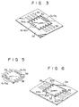
- IC pellet 32 containing the IC (Fig. 2) is put within recess 34a made in base plate 34 of card body 10, and is then so positioned to have eight pads 12 aligned with leads 30, respectively. Leads 30 are then bonded to pads 12.
- the data including secret data stored in EEP-ROM 22 could be read merely by touching a test probe to data pads D1 to Dn and address pads A1 to Am, which remained intact. In other words, the IC card could be forged based on the data thus read from EEP-ROM 22. This greatly reduces the security of the IC card. In the worst possible case, the technical aspects of the IC card system as a whole can be analyzed and unlawfully utilized on a large scale.
- connection pads to the memory bus, which are only usable during test operations after manufacturing the integrated circuit chip on a wafer, but which connections are separated or destroyed when the wafer is cut into separate chips. This is particularly done by placing the connection pads connected to a memory bus of one chip on the area of the adjacent chip, so that the connections are automatically destroyed when cutting the wafer into chips. Moreover, it is indicated that these connections could also be separated if they were formed as fusible poly links, or the separation could be performed by laser beams.
- an IC card of the kind defined is characterized by comparator means for comparing an address input via the data input/output terminal means with a predetermined address, and for generating a coincidence signal upon agreement; and gate means coupled between at least one of said test data terminals and said data bus and/or between said test address terminals and said address bus, for disconnecting at least one of the test terminals when the coincidence signal of said comparator means is present, whereby after the completion of said test operation even when the access command is applied to said test address terminals, and secret data is thus unobtainable from said test data terminals.
- the invention also relates to a method of manufacturing an IC card as defined by claim 6.
- step S1 the card manufacturer forms an IC on a wafer. This IC is similar to the one shown in Fig. 2.
- step S2 the manufacturer tests the IC. To be more precise, a test probe is put into contact with the exposed test data pads and test address pads of the IC, thereby accomplishing various tests. (As described above, the test data pads are coupled to the data bus connecting the CPU and EEP-ROM both included in the IC, and the test address pads are coupled to the address bus connecting the CPU and EEP-ROM.)
- step S3 the wafer is diced into a plurality of IC pellets.
- step S4 the test data pads and test address pads, which are no longer necessary, are removed from each IC pellet, or disconnected from the data bus and address bus formed in the IC pellet.
- Test(data pads D1 to Dn and test address pads A1 to Am are removed by cutting the opposing edge portions of IC pellet 32, on which test pads D1 to Dn and test address pads A1 to Am are formed, along the one- dot-one-dash lines shown in Fig. 5.
- Eight connection pads 38 which will be electrically connected to pads 12 (Fig. 1), are formed on other opposing edge portions of IC pellet 32.
- IC pellet can be cut to remove the test data pads and test address pads, by applying a laser beam or an etching solution to IC pellet 32.
- step S5 die-bonding is carried out to bond IC pellet 32 to base plate 34, and wire- bonding is performed to bond leads 30 to pads 38. More specifically, as shown in Fig. 6, IC pellet 32 is placed in recess 34a made in base plate 34 and is positioned to have pads 38 aligned with the ends (30a) of leads 30. IC pellet 32 is then die-bonded to base plate 34, and pins 38 of IC pellet 32 are connected to ends 30a of leads 30 by hot-pressing or pulse-heating process.
- step S6 a resin is applied onto the major surface of base plate 34, in which IC pellet 32 is now provided, thereby achieving the plasticsealing of IC pellet 32.
- test data is written in the test data area of the memory section of IC pellet 32, in step S7, through input/output terminal 1/0.
- the test data is a minimal amount of data that is required for the fundamental operation of the IC card.
- step S8 the IC pellet is subjected to the final test. Namely, basic tests on codes such as PIN (later described) are carried out.
- step S9 the unit consisting of IC pellet 32, base plate 34 and leads 30 is built in an IC card body.
- the IC card body comprises upper sheet 42, intermediate sheet 44 and lower sheet 46, which are put one upon another and bonded together.
- intermediate sheet 44 made of hardy PVC is bonded to lower sheet 46 made of soft PVC.
- Sheet 44 has an opening. This opening forms a recess 44a when sheet 44 and 46 are bonded.
- the base plate 34 is bonded to sheet 42, forming an IC assembly.
- Upper sheet 42 made of soft PVC has eight through holes, arranged in two rows, each row consisting of four holes. Eight contacts 42a are formed in these holes.
- the IC assembly is positioned within recess 44a such that the IC unit contacts lower sheet 46.
- upper shect 42 is bonded to intermediate sheet 44, such that contacts 42a are connected to base plate 34.
- the IC card body is formed.
- a magnetic stripe (not shown in Fig. 7) is bonded on upper sheet 42.
- an IC card is manufactured.
- This IC card has the same outer appearance as the conventional IC card shown in Fig. 1.
- step S10 the card manufacturer inserts the IC card into a manufacturer's card terminal, and operates the manufacturer's card terminal, thereby writing codes CA (Card Authenticator), IPIN (Initialization Personal Identification Number), PMK (Production Master Key) and PRK (Private Key) into EEP-ROM 22.
- Code CA will be used to encrypt and decrypt messages.
- Code IPIN is a 6- bit code which remains valid until code PIN (Personal Identification Number) is written into EEP-ROM 22.
- Code PMK represents the number assigned to IC cards of the same lot. Code PRK will be used to decrypt an encrypted message.
- step S11 the card manufacturer mails the IC card and the PMK-printed paper to the card issuer under separate cover. Here, the card manufacturer has finished all work required of him.
- the card issuer inserts the IC card into an issuer's card terminal, and operates the issuer's card terminal, thereby inputting code PAN representing the primary account number assigned to the cardholder, and also inputting code PMK printed the sheet of paper mailed from the card manufacturer.
- Code PAN is written into EEP-ROM 22 in step S12 only when code PMK is identical with code PMK written in EEP-ROM 22 in step S10.
- the issuer's card terminal reads code IPIN from EEP-ROM 22 and prints this code on a sheet of paper.
- the card issuer mails the IC card and the IPIN-printed paper to the cardholder.
- the cardholder takes the IC card and the IPIN-printed paper to the card issuer's office.
- the cardholder inserts the IC card in the card terminal installed in the card issuer's office, and then operates the card terminal, thereby inputting his or her personal identification number (PIN) and also code IPIN printed on the paper mailed from the card issuer.
- PIN personal identification number
- Code PIN is written into EEP-ROM 22 only when code IPIN is identical with code IPIN already written in EEP-ROM 22. After code PIN has been thus written into EEP-ROM 22, the IC card can be used.
- test data pads and test address pads are removed from the IC pellet after the IC chip has been tested. Therefore, if the IC card containing this IC pellet chances to fall into the hands of anyone other than the cardholder by theft or loss, and if the IC pellet is removed from the IC card, the data stored in EEP-ROM 22 can by no means be read. This prevents a forgery of the IC card, and ultimately maintains not only the security of the IC card, but also the security of the IC card system. Not all the test pads need be removed after the test of the IC pellet. For instance, it suffices to remove only the test data pads, only the test address pads or only some of the test data pads or test address pads.
- pads 38 are wirebonded to leads 30 in step S5. Without such wirebonding, pads 38 can be connected to leads 30 as in the modification (i.e., an IC pellet) shown in Fig. 8.
- this IC pellet comprises silicon substrate 52, active region 54 formed in the surface of substrate 52, insulation layer 56 formed on the surface of substrate 52 and having contact holes, inner contact pad 58 formed on insulation layer 56 and electrically connected to active region 54 through the contact holes of insulation layer 56, insulation layer 60 formed on inner contact pad 58 and having contact holes, and outer contact pad 62 formed on insulation layer 60 and electrically connected to inner contact pad 58 through the contact holes of insulation layer 60.
- This IC pellet (Fig.
- the anisotropically conductive adhesive consists of a hot-melt insulative adhesive and electrically conductive particles of nickel, silver or carbon, dispersed within the adhesive. It allows the passage of an electric current only in the direction in which it is compressed by hot-pressing.
- outer contact pad 62 is extremely narrow, no conductive particles contained in the anisotropically conductive adhesive can contact pad 62. If this is the case, no electrical connection is accomplished between the IC pellet (Fig. 8) and the base plate. Therefore, in the modification of Fig. 8, outer contact pad 62 is broad enough to ensure the electrical connection between the IC pellet and the base plate. Since no wire-bonding is required in connecting the IC pellet to the base plate, the IC pellet can be efficiently connected to the base plate.
- the internal circuit comprises a system bus 151 comprising an address bus 26 and a data bus 24.
- Data ROM 152, application ROM 153, system program ROM 154, working RAM 155, system control-ler 156, decryption unit 157, and read/write controller 158 are coupled to system bus 151.
- Input buffer 159 is connected to system bus 151, and input controller 160 is coupled to input buffer 159.
- Output buffer 161 is connected to system bus 151, and output controller 162 is connected to output buffer 161.
- Data input/output terminal I/O is connected to input controller 160 and also to output controller 162.
- Data ROM 152 stores data representing all operation conditions of the IC cards, such as data- writing voltage, current tolerance, maximum application time, maximum data transmission capacity, and maximum response-waiting time.
- the condition data is supplied as "answer-to-reset" data to a card terminal (not shown) in conformance with a preset format.
- Application RON 153 stores code APN (Application Name) showing the classification of the IC card. Code APN is put into a specified format and then supplied to the card terminal when an attribute exchange takes place in the card terminal after initial parameters have been set in the card terminal in accordance with the answerto-reset data.
- System program ROM 154 stores codes ACK (acknowledgment) and NAC (non-aknowledgment), as well as every kind of system program.
- Code ACK indicates that the signal transmitted from the card terminal to the IC card is correct, and code NAC shows that this signal is incorrect.
- System controller 156 has an internal decision area. Controller 156 outputs commands to the associated components included in the internal circuit of the IC card, in accordance with the data supplied from input buffer 159 and in accordance with the operation status of the IC card.
- Decryption unit 157 decrypts the input data supplied from the card terminal through input buffer 159, in accordance with an RSA algorithm. It uses the decryption key code (the card issuer's private key) stored in key code memory 157a.
- Unit 157 outputs the decrypted data to comparator 163.
- the output data of comparator 163 is supplied to system controller 156 through system control line 156a.
- System control line 156a is connected to flag 164.
- Flag 164 is set or reset by the output data of comparator 163.
- Read/ write controller 158 controls the data-writing and data-reading from data memory 165 in accordance with the command supplied from system controller 156.
- the data read from data memory 165 under the control of read/write controller 158 is input to comparator 163, system bus 151 or card status buffer 166.
- Read/write controller 158 has a tri-state gate 181.
- Tri-state gate 181 is connected on data lines 182 to which the test data pads (not shown in Fig. 9) of the IC card are connected.
- Flag section 183 comprised of a one-bit memory is connected to read/write controller 158.
- the output of comparator 168 is coupled to a set terminal of flag section 183 as a fetch signal.
- the output signal of flag-setting section 183 is supplied to inverter 184.
- the output of inverter 184 is supplied to the control terminal of tri-state gate 181 and also to the input terminal of flag section 183.
- Data memory 165 is, for example, an EEP-ROM.
- Secret codes CA, IPIN, PAN, CHN, EPD, PRK and RTN, and status data ST are written in this memory.
- Code CHN represents the cardholder's name
- code EPD shows the expiration data of the IC card.
- Code RTN indicates the number of times any incorrect data has been input to the IC card.
- Status data ST represents the present status of the IC card. More precisely, data ST shows whether the IC card has been completely manufactured, duly issued, or made usable by entering code PIN.
- Status data ST is in the same format as code APN (Application Name) stored in application ROM 153. Data ST is transmitted to the card terminal.
- Data memory 165 is not limited to an EEP-ROM; it can be comprised of an EP-ROM (Erasable Programmable - Read Only Memory), for instance.
- System controller 156 is connected to timer 167.
- This timer 167 counts a predetermined period of time during the normal data exchange between the IC card and the card terminal, when a start data write voltage supply message is output by the card terminal. If a positive response code ACK is not supplied from the card terminal to the IC card during said period of time, system controller 156 stops the data exchange between the IC card and the card terminal.
- Read/write controller 158 is connected to system bus 151 by a bus line. This bus line is coupled to one of the two input terminals of address comparator 168. Fixed address unit 169 is connected to the other input terminal of address comparator 168. Unit 169 stores a specific address of memory 165 that is not used. Address comparator 168 compares any address supplied to it via system bus 151 with the address stored in fixed address unit 169. The output data of comparator 168 is supplied to read/write controller 158 and also to the set terminal of flag section 183.
- address comparator 168 When the two addresses compared by address comparator 168 are the same, that is, when the card terminal has input an illegal address, address comparator 168 generates a coincidence signal and read/write control- ler 158 clears all data stored in data memory 165, thereby preventing secret data from being read out of the card.
- a reset signal RESET and a system clock signal are supplied from the card terminal to the IC card through connection pads.
- Voltages Vcc and Vpp are applied from the card terminal to the IC card. Voltage Vcc is used to drive both the IC card and the card terminal, and voltage Vpp is used to write data into data memory 165.
- the card terminal starts applying these voltages to the IC card in response to the answer-to-reset data read from data ROM 152.
- the system clock signal supplied to the IC card is.frequency-divided by frequency divider 170.
- the card terminal supplies an initialization signal to the IC card.
- system controller 156 reads the answer-to-reset data from data ROM 152.
- the answer-to-reset data is supplied to the card terminal through output buffer 161, output controller 162 and input/output terminal 1/0.
- the card terminal sends an enquiry code (ENQ) to the IC card.
- Code ENQ is input to working RAM 155 through input-output terminal 1/0, input controller 160 and input buffer 159.
- System controller 156 determines whether or not code ENQ has been correctly written into working RAM 155. If it determines that code ENQ has been correctly written, system controller 156 supplies code ACK to the card terminal through output buffer 161, output controller 162 and input/output terminal 1/0. If system controller 156 determines that code ENQ has been incorrectly written, it supplies code NAC to the card terminal.
- the card terminal In response to code ACK, the card terminal sends terminal code TC representing the type of the card terminal to the IC card. In response to code NAC, the card terminal ejects the IC card, thereby electrically disconnecting the IC card from it.
- code APN Application Name showing the type of the IC card is read from application ROM 153 under the control of system controller 156. Code APN is temporarily latched in output buffer 161 and is then sent to the card terminal.
- the card terminal determines, from code APN, whether or not the IC card is compatible with the card terminal. If the IC card is found to be compatible, the card terminal sends a command code to the IC card. Conversely, if the IC card is found to be incompatible, the card terminal ejects the IC card, thereby electrically disconnecting the IC card from it.
- code PIN Personal Identification Number
- step S100 data memory 165 is tested for its function. More specifically, a test probe is put into contact with the test data pads connected to data lines 182 and the test address pads connected to address lines 150, as in the test of the IC pellet built in the IC card of the solution of figures 4 and 5. Since flag section 183 is set to "0,” the output of inverter 184 is "1.” Tri-state gate 181 is therefore conductive.
- step S102 the address data identical with the address stored in fixed address unit 169 is input to comparator 168 through system bus 151 in step S102.
- the output of comparator 168 becomes "1," whereby a signal for reading the output of inverter 184 is supplied to flag-setting section 183 through line 185 connecting compa-rator 168 to flag section 183.
- step S104 the output of inverter 184, i.e., "1,” is sent to flag section 183.
- the output of inverter 184 therefore changes to "0,” and tri-state gate 181 becomes inconductive. Consequently, data lines 182 are electrically cut, and the test data pads, which are coupled to these data lines 182, are electrically disconnected from data memory 165.
- the IC pellet is built in an IC card body, whereby the IC card is completed.
- step S110 it is determined whether or not a command for an access to data memory 165 has been supplied to the IC card. If YES, a data memory address is generated in step S112. In the next step, step S114, it is determined whether or not address comparator 168 has found that this address is identical with the address stored in fixed address unit 169. If NO in step S114, an access is made to data memory 165, in step S116. If YES in step S114, read/ write controller 158 clears the data stored in data memory 165 in step S118.
- the two addresses compared by comparator 168 can be identical also when tri-state gate 181 is rendered inconductive after the IC pellet has been tested. Nonetheless, when the data set in flag section 183 is "0" and tri-state gate 181 is made conductive, the data stored in memory 165 is not cleared. Data memory 165 is cleared only when both the output of comparator 168 and the data set in flag section 183 are "1.”
- All data stored in data memory 165 is cleared when the address set in fixed address unit 169 which is not provided in data memory 165 is supplied to the IC card. Therefore, the data cannot be illegally read from data memory 165.
- tri-state gate 181 is used to electrically cut data lines 182, thereby electrically disconnecting the test data pads from data memory 165. Any other means, such as a gate or a switch, can be used for the same purpose. Further, tri-state gate 181 can be replaced by a fuse which is physically cut, thereby to permanently cut data lines 182. Still further, a tri-state gate can be connected between address lines 150 and system bus 151 for electrically connecting or disconnecting the test address pads to or from data memory 165, either in place of, or in addition to, tristate gate 181. Further, plural unused memory addresses may be stored in fixed address unit 169.
- the test data pads are disconnected from the data lines 182 or the test address pads are cut from the address lines 150, after the IC pellet has been tested.
- all test pads are disconnected from the data lines and address lines after the test of the IC pellet. Therefore, an illegal access to the data memory provided within the IC card is prevented, ensuring not only the security of the IC card, but also that of the IC card system.
Description
- The present invention relates to an IC card (integrated circuit card) comprising data input/ output terminal means; memory means wherein direct access to at least a portion of the memory means is prevented, said memory means storing secret data when input to said memory means through said data input/output terminal means, said memory means being arranged to output the secret data in response to an access command made indirectly via the data input/output terminal means; an address bus and a data bus associated with said memory means; test address terminals connected to the address bus of said memory means, for enabling addresses of the memory means to be accessed during a test operation; test data terminals arranged to be connected to the data bus of said memory means, for enabling inputting of data to and outputting of data from the memory means during said test operation; and the test address terminals being disconnected from the address bus and/or the test data test terminals being disconnected from the data bus after the completion of the test operation.
- Recent years have been called "the cashless era." Many things can be bought by using personal identification (ID) cards issued by credit companies and the like, eliminating the need to pay in cash.
- Various kinds of ID cards are available at present, such as plastic cards, embossed cards, and cards with a magnetic stripe. From a structural point of view, these cards are easy to forge. Further, the data recorded on them can be easily read. Many cases of their illegal use have been reported, and this has become a great social problem.
- To resolve this problem, IC cards with a built-in CPU and a built-in IC memory have been developed. The IC memory stores various data about the card owner, such as his or her personal identification number. The data cannot be easily read from the IC memory. Recently, an IC card system comprising such IC cards and terminals has been put to practical use.
- Fig. 1 is a perspective view of an IC card. As shown in this figure, eight
connection pads 12 are arranged onplastic card body 10, in two vertical rows, each consisting of four pads. When the IC card is inserted in a terminal,connection pads 12 contact the corresponding pins provided in the terminal, thereby electrically connecting the IC card to the terminal. Of these eight pads, only six are actually used at present.Magnetic stripe 14 is adhered to the surface ofcard body 10. - An integrated circuit (IC) of the structure shown in Fig. 2 is formed within
card body 10. This IC comprises CPU (Central Processing Unit) 20 and EEP-ROM (Electrically Erasable Programmable - Read Only Memory) 22. The six connection pads, i.e., input/output terminal 1/0, clock terminal CLOCK, reset terminal RESET, power supply terminal Vcc, ground terminal GND and datawriting power supply terminal Vpp, are provided in the IC. Due to its specific use, the IC must be greatly reliable. Therefore, it is subjected to an extremely strict test before delivery. EEP-ROM 22 is tested by inputting data to it, and outputting data from it, through input/output terminal 1/0, bit by bit. Obviously, this method of testing EEP-ROM 22 requires too long a time. To save time, data pads D1 to Dn are coupled to n-bit data bus 24 connectingCPU 20 and EEP-ROM 22, and address pads A1 to Am are coupled to m-bit address bus 26 connectingCPU 20 and EEP-ROM 22. The test probe designed to test EEP-ROM 22 is put into contact with data pads D1 to Dn and address pads A1 to Am, whereby EEP-ROM 22 can be tested within a short time. - After EEP-
ROM 22 has been tested, only leads 30 are bonded to eightpads 12 as illustrated in Fig. 3, but no process is performed on data pads D1 to Dn or address pads A1 to Am. Thereafter, the IC is incorporated intocard body 10. More precisely,IC pellet 32 containing the IC (Fig. 2) is put withinrecess 34a made inbase plate 34 ofcard body 10, and is then so positioned to have eightpads 12 aligned withleads 30, respectively.Leads 30 are then bonded to pads 12. - If the IC card happens to fall into the hands of a person other than the card owner, either by theft or loss, and if the IC is removed from
card body 10, the data including secret data stored in EEP-ROM 22 could be read merely by touching a test probe to data pads D1 to Dn and address pads A1 to Am, which remained intact. In other words, the IC card could be forged based on the data thus read from EEP-ROM 22. This greatly reduces the security of the IC card. In the worst possible case, the technical aspects of the IC card system as a whole can be analyzed and unlawfully utilized on a large scale. - From WO 83/00244 it is already known to disable direct access to a memory, particularly in connection with credit or security cards, by providing connection pads to the memory bus, which are only usable during test operations after manufacturing the integrated circuit chip on a wafer, but which connections are separated or destroyed when the wafer is cut into separate chips. This is particularly done by placing the connection pads connected to a memory bus of one chip on the area of the adjacent chip, so that the connections are automatically destroyed when cutting the wafer into chips. Moreover, it is indicated that these connections could also be separated if they were formed as fusible poly links, or the separation could be performed by laser beams.
- It is an object of the invention to provide an IC card in which this step of separating the connections to test address terminals and test data terminals is more flexibly performed, so that the internal data cannot be illegally read, thereby maintaining the security of not only the card but also the system in which the card is used.
- According to the invention as defined by claim 1, an IC card of the kind defined is characterized by comparator means for comparing an address input via the data input/output terminal means with a predetermined address, and for generating a coincidence signal upon agreement; and gate means coupled between at least one of said test data terminals and said data bus and/or between said test address terminals and said address bus, for disconnecting at least one of the test terminals when the coincidence signal of said comparator means is present, whereby after the completion of said test operation even when the access command is applied to said test address terminals, and secret data is thus unobtainable from said test data terminals.
- The invention also relates to a method of manufacturing an IC card as defined by claim 6.
- Preferable embodiments are defined in the dependent claims.
- This invention can be more fully understood from the following detailed description when taken in conjunction with the accompanying drawings, in which:
- Figure 1 is a perspective view of an IC card;
- Figure 2 shows the internal circuit of the IC card shown in figure 1;
- Figure 3 is a diagram representing the connection between the IC pellet and base plate of a conventional IC card;
- Figure 4 is a flow chart explaining the process of manufacturing an IC card with mechanical disconnection of the test pads;
- Figure 5 is a perspective view of the IC pellet used in the IC card according to the solution of figure 4;
- Figure 6 is a diagram illustrating the connection between the IC pellet and base plate of the IC card according to the solution of figures 4 and 5;
- Figure 7 is a cross-sectional view of the IC card according to the solution of figures 4 and 5;
- Figure 8 is a cross-sectional view of the IC card which is a modification;
- Figure 9 shows the internal circuit of the IC card according to an embodiment of this invention;
- Figure 10 is a flow chart explaining the process of manufacturing the IC card according to the embodiment of figure 9; and
- Figure 11 is a flow chart explaining the operation of the IC card according to the invention.
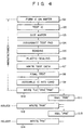
- First, it will be explained how the IC card, e.g., a credit card, is manufactured with reference to the flow chart of figure 4.
- To manufacture an IC card and bring it into a usable condition, a card manufacturer, a card issuer and a cardholder all take part in the process. In step S1, the card manufacturer forms an IC on a wafer. This IC is similar to the one shown in Fig. 2.
- In step S2, the manufacturer tests the IC. To be more precise, a test probe is put into contact with the exposed test data pads and test address pads of the IC, thereby accomplishing various tests. (As described above, the test data pads are coupled to the data bus connecting the CPU and EEP-ROM both included in the IC, and the test address pads are coupled to the address bus connecting the CPU and EEP-ROM.) In the next step, step S3, the wafer is diced into a plurality of IC pellets. In step S4, the test data pads and test address pads, which are no longer necessary, are removed from each IC pellet, or disconnected from the data bus and address bus formed in the IC pellet. Now, only one terminal i.e., input/output terminal 1/0, through which data in the EEP-ROM can be read out, is connected to the IC. This prevents an illegal access to the EEP-ROM. Test(data pads D1 to Dn and test address pads A1 to Am are removed by cutting the opposing edge portions of
IC pellet 32, on which test pads D1 to Dn and test address pads A1 to Am are formed, along the one- dot-one-dash lines shown in Fig. 5. Eightconnection pads 38, which will be electrically connected to pads 12 (Fig. 1), are formed on other opposing edge portions ofIC pellet 32. IC pellet can be cut to remove the test data pads and test address pads, by applying a laser beam or an etching solution toIC pellet 32. - Thereafter, in step S5, die-bonding is carried out to bond
IC pellet 32 tobase plate 34, and wire- bonding is performed to bond leads 30 topads 38. More specifically, as shown in Fig. 6,IC pellet 32 is placed inrecess 34a made inbase plate 34 and is positioned to havepads 38 aligned with the ends (30a) of leads 30.IC pellet 32 is then die-bonded tobase plate 34, and pins 38 ofIC pellet 32 are connected to ends 30a ofleads 30 by hot-pressing or pulse-heating process. - In the next step, step S6, a resin is applied onto the major surface of
base plate 34, in whichIC pellet 32 is now provided, thereby achieving the plasticsealing ofIC pellet 32. Then, test data is written in the test data area of the memory section ofIC pellet 32, in step S7, through input/output terminal 1/0. The test data is a minimal amount of data that is required for the fundamental operation of the IC card. - Then, in step S8, the IC pellet is subjected to the final test. Namely, basic tests on codes such as PIN (later described) are carried out.
- In step S9, the unit consisting of
IC pellet 32,base plate 34 and leads 30 is built in an IC card body. As shown in Fig. 7, the IC card body comprisesupper sheet 42,intermediate sheet 44 andlower sheet 46, which are put one upon another and bonded together. To be more precise,intermediate sheet 44 made of hardy PVC is bonded tolower sheet 46 made of soft PVC.Sheet 44 has an opening. This opening forms a recess 44a whensheet base plate 34 is bonded tosheet 42, forming an IC assembly.Upper sheet 42 made of soft PVC has eight through holes, arranged in two rows, each row consisting of four holes. Eight contacts 42a are formed in these holes. The IC assembly is positioned within recess 44a such that the IC unit contactslower sheet 46. Then,upper shect 42 is bonded tointermediate sheet 44, such that contacts 42a are connected tobase plate 34. As a result, the IC card body is formed. A magnetic stripe (not shown in Fig. 7) is bonded onupper sheet 42. As a result, an IC card is manufactured. This IC card has the same outer appearance as the conventional IC card shown in Fig. 1. - Thereafter, in step S10, the card manufacturer inserts the IC card into a manufacturer's card terminal, and operates the manufacturer's card terminal, thereby writing codes CA (Card Authenticator), IPIN (Initialization Personal Identification Number), PMK (Production Master Key) and PRK (Private Key) into EEP-
ROM 22. Code CA will be used to encrypt and decrypt messages. Code IPIN is a 6- bit code which remains valid until code PIN (Personal Identification Number) is written into EEP-ROM 22. Code PMK represents the number assigned to IC cards of the same lot. Code PRK will be used to decrypt an encrypted message. - After codes CA, IPIN, PMK and PRK have been written into EEP-
ROM 22, the manufacturer's card terminal prints code PMK on a sheet of paper. In step S11, the card manufacturer mails the IC card and the PMK-printed paper to the card issuer under separate cover. Here, the card manufacturer has finished all work required of him. - The card issuer inserts the IC card into an issuer's card terminal, and operates the issuer's card terminal, thereby inputting code PAN representing the primary account number assigned to the cardholder, and also inputting code PMK printed the sheet of paper mailed from the card manufacturer. Code PAN is written into EEP-
ROM 22 in step S12 only when code PMK is identical with code PMK written in EEP-ROM 22 in step S10. When code PAN is written into EEP-ROM 22, the issuer's card terminal reads code IPIN from EEP-ROM 22 and prints this code on a sheet of paper. In step S13, the card issuer mails the IC card and the IPIN-printed paper to the cardholder. - The cardholder takes the IC card and the IPIN-printed paper to the card issuer's office. In step S14, the cardholder inserts the IC card in the card terminal installed in the card issuer's office, and then operates the card terminal, thereby inputting his or her personal identification number (PIN) and also code IPIN printed on the paper mailed from the card issuer. Code PIN is written into EEP-
ROM 22 only when code IPIN is identical with code IPIN already written in EEP-ROM 22. After code PIN has been thus written into EEP-ROM 22, the IC card can be used. - Before delivery the test data pads and test address pads are removed from the IC pellet after the IC chip has been tested. Therefore, if the IC card containing this IC pellet chances to fall into the hands of anyone other than the cardholder by theft or loss, and if the IC pellet is removed from the IC card, the data stored in EEP-
ROM 22 can by no means be read. This prevents a forgery of the IC card, and ultimately maintains not only the security of the IC card, but also the security of the IC card system. Not all the test pads need be removed after the test of the IC pellet. For instance, it suffices to remove only the test data pads, only the test address pads or only some of the test data pads or test address pads. - A modification will now be described. In the first solution,
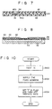
pads 38 are wirebonded to leads 30 in step S5. Without such wirebonding,pads 38 can be connected to leads 30 as in the modification (i.e., an IC pellet) shown in Fig. 8. As illustrated in Fig. 8, which is a cross-sectional view, this IC pellet comprisessilicon substrate 52,active region 54 formed in the surface ofsubstrate 52,insulation layer 56 formed on the surface ofsubstrate 52 and having contact holes,inner contact pad 58 formed oninsulation layer 56 and electrically connected toactive region 54 through the contact holes ofinsulation layer 56,insulation layer 60 formed oninner contact pad 58 and having contact holes, andouter contact pad 62 formed oninsulation layer 60 and electrically connected toinner contact pad 58 through the contact holes ofinsulation layer 60. This IC pellet (Fig. 8) is adhered to a base plate with an anisotropically conducive adhesive. The unit consisting of the IC pellet and base plate is incorporated into an IC card body, thereby forming an IC card. The anisotropically conductive adhesive consists of a hot-melt insulative adhesive and electrically conductive particles of nickel, silver or carbon, dispersed within the adhesive. It allows the passage of an electric current only in the direction in which it is compressed by hot-pressing. Whenouter contact pad 62 is extremely narrow, no conductive particles contained in the anisotropically conductive adhesive can contactpad 62. If this is the case, no electrical connection is accomplished between the IC pellet (Fig. 8) and the base plate. Therefore, in the modification of Fig. 8,outer contact pad 62 is broad enough to ensure the electrical connection between the IC pellet and the base plate. Since no wire-bonding is required in connecting the IC pellet to the base plate, the IC pellet can be efficiently connected to the base plate. - An embodiment of the present invention will now be described with reference to the circuit diagram of Fig. 9, which shows the internal circuit of the IC card.
- As shown in Fig.9, the internal circuit comprises a
system bus 151 comprising anaddress bus 26 and adata bus 24.Data ROM 152,application ROM 153,system program ROM 154, workingRAM 155, system control-ler 156,decryption unit 157, and read/write controller 158 are coupled tosystem bus 151.Input buffer 159 is connected tosystem bus 151, andinput controller 160 is coupled to inputbuffer 159.Output buffer 161 is connected tosystem bus 151, andoutput controller 162 is connected tooutput buffer 161. Data input/output terminal I/O is connected to inputcontroller 160 and also tooutput controller 162. -
Data ROM 152 stores data representing all operation conditions of the IC cards, such as data- writing voltage, current tolerance, maximum application time, maximum data transmission capacity, and maximum response-waiting time. When the IC card is initialized, the condition data is supplied as "answer-to-reset" data to a card terminal (not shown) in conformance with a preset format.Application RON 153 stores code APN (Application Name) showing the classification of the IC card. Code APN is put into a specified format and then supplied to the card terminal when an attribute exchange takes place in the card terminal after initial parameters have been set in the card terminal in accordance with the answerto-reset data.System program ROM 154 stores codes ACK (acknowledgment) and NAC (non-aknowledgment), as well as every kind of system program. Code ACK indicates that the signal transmitted from the card terminal to the IC card is correct, and code NAC shows that this signal is incorrect.System controller 156 has an internal decision area.Controller 156 outputs commands to the associated components included in the internal circuit of the IC card, in accordance with the data supplied frominput buffer 159 and in accordance with the operation status of the IC card.Decryption unit 157 decrypts the input data supplied from the card terminal throughinput buffer 159, in accordance with an RSA algorithm. It uses the decryption key code (the card issuer's private key) stored in key code memory 157a.Unit 157 outputs the decrypted data tocomparator 163. The output data ofcomparator 163 is supplied tosystem controller 156 through system control line 156a. System control line 156a is connected toflag 164.Flag 164 is set or reset by the output data ofcomparator 163. Read/write controller 158 controls the data-writing and data-reading from data memory 165 in accordance with the command supplied fromsystem controller 156. The data read from data memory 165 under the control of read/write controller 158 is input tocomparator 163,system bus 151 orcard status buffer 166. Read/write controller 158 has atri-state gate 181.Tri-state gate 181 is connected on data lines 182 to which the test data pads (not shown in Fig. 9) of the IC card are connected. -
Flag section 183 comprised of a one-bit memory is connected to read/write controller 158. The output ofcomparator 168 is coupled to a set terminal offlag section 183 as a fetch signal. The output signal of flag-settingsection 183 is supplied toinverter 184. The output ofinverter 184 is supplied to the control terminal oftri-state gate 181 and also to the input terminal offlag section 183. - Data memory 165 is, for example, an EEP-ROM. Secret codes CA, IPIN, PAN, CHN, EPD, PRK and RTN, and status data ST are written in this memory. Code CHN represents the cardholder's name, and code EPD shows the expiration data of the IC card. Code RTN indicates the number of times any incorrect data has been input to the IC card. Status data ST represents the present status of the IC card. More precisely, data ST shows whether the IC card has been completely manufactured, duly issued, or made usable by entering code PIN. Status data ST is in the same format as code APN (Application Name) stored in
application ROM 153. Data ST is transmitted to the card terminal. Data memory 165 is not limited to an EEP-ROM; it can be comprised of an EP-ROM (Erasable Programmable - Read Only Memory), for instance. -
System controller 156 is connected totimer 167. Thistimer 167 counts a predetermined period of time during the normal data exchange between the IC card and the card terminal, when a start data write voltage supply message is output by the card terminal. If a positive response code ACK is not supplied from the card terminal to the IC card during said period of time,system controller 156 stops the data exchange between the IC card and the card terminal. - Read/
write controller 158 is connected tosystem bus 151 by a bus line. This bus line is coupled to one of the two input terminals ofaddress comparator 168. Fixedaddress unit 169 is connected to the other input terminal ofaddress comparator 168.Unit 169 stores a specific address of memory 165 that is not used.Address comparator 168 compares any address supplied to it viasystem bus 151 with the address stored in fixedaddress unit 169. The output data ofcomparator 168 is supplied to read/write controller 158 and also to the set terminal offlag section 183. When the two addresses compared byaddress comparator 168 are the same, that is, when the card terminal has input an illegal address, addresscomparator 168 generates a coincidence signal and read/write control-ler 158 clears all data stored in data memory 165, thereby preventing secret data from being read out of the card. - When the IC card is electrically coupled to the card terminal, a reset signal RESET and a system clock signal are supplied from the card terminal to the IC card through connection pads. Voltages Vcc and Vpp are applied from the card terminal to the IC card. Voltage Vcc is used to drive both the IC card and the card terminal, and voltage Vpp is used to write data into data memory 165. The card terminal starts applying these voltages to the IC card in response to the answer-to-reset data read from
data ROM 152. The system clock signal supplied to the IC card is.frequency-divided byfrequency divider 170. - The data exchange between the IC card shown in Fig. 9 and the card terminal will now be explained. When the IC card is inserted into the card terminal and thus electrically connected thereto, the card terminal supplies an initialization signal to the IC card. In response to the initialization signal,
system controller 156 reads the answer-to-reset data fromdata ROM 152. The answer-to-reset data is supplied to the card terminal throughoutput buffer 161,output controller 162 and input/output terminal 1/0. - If the answer-to-reset data is found to be correct, the card terminal sends an enquiry code (ENQ) to the IC card. Code ENQ is input to working
RAM 155 through input-output terminal 1/0,input controller 160 andinput buffer 159.System controller 156 determines whether or not code ENQ has been correctly written into workingRAM 155. If it determines that code ENQ has been correctly written,system controller 156 supplies code ACK to the card terminal throughoutput buffer 161,output controller 162 and input/output terminal 1/0. Ifsystem controller 156 determines that code ENQ has been incorrectly written, it supplies code NAC to the card terminal. - In response to code ACK, the card terminal sends terminal code TC representing the type of the card terminal to the IC card. In response to code NAC, the card terminal ejects the IC card, thereby electrically disconnecting the IC card from it.
- When terminal code TC is supplied to the IC card, code APN (Application Name) showing the type of the IC card is read from
application ROM 153 under the control ofsystem controller 156. Code APN is temporarily latched inoutput buffer 161 and is then sent to the card terminal. - The card terminal determines, from code APN, whether or not the IC card is compatible with the card terminal. If the IC card is found to be compatible, the card terminal sends a command code to the IC card. Conversely, if the IC card is found to be incompatible, the card terminal ejects the IC card, thereby electrically disconnecting the IC card from it.
- When the command code is supplied to the IC card, code PIN (Personal Identification Number) stored in the IC card is compared with code PIN input through the keyboard of the card terminal. If these compared codes are identical, data will be exchanged between the IC card and the card terminal, thereby enabling a financial transaction.
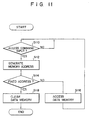
- With reference to the flow chart of Fig. 10, it will be briefly explained how the IC card of the embodiment is manufactured. First, in step S100, data memory 165 is tested for its function. More specifically, a test probe is put into contact with the test data pads connected to data lines 182 and the test address pads connected to address
lines 150, as in the test of the IC pellet built in the IC card of the solution of figures 4 and 5. Sinceflag section 183 is set to "0," the output ofinverter 184 is "1."Tri-state gate 181 is therefore conductive. Hence, the data stored in those addresses of data memory 165 which have been designated by the signals supplied from the test probe through the test address pads,address lines 150 andsystem bus 151, is read out to the test data pads coupled to data lines 182, throughtri-state gate 181 of read/write controller 158. Data memory 165 is thereby tested. - Upon completion of the test of data memory 165, the address data identical with the address stored in fixed
address unit 169 is input tocomparator 168 throughsystem bus 151 in step S102. As a result, the output ofcomparator 168 becomes "1," whereby a signal for reading the output ofinverter 184 is supplied to flag-settingsection 183 throughline 185 connecting compa-rator 168 toflag section 183. Then, in step S104, the output ofinverter 184, i.e., "1," is sent toflag section 183. The output ofinverter 184 therefore changes to "0," andtri-state gate 181 becomes inconductive. Consequently, data lines 182 are electrically cut, and the test data pads, which are coupled to these data lines 182, are electrically disconnected from data memory 165. Thereafter, the IC pellet is built in an IC card body, whereby the IC card is completed. - If any person other than the cardholder receives this IC card by theft or by chance, he or she has no way to access to data memory 165 since the data pads have been disconnected from data lines 182. In short, an illegal reading of the data from data memory 165 can be prevented. This ensures not only the security of the IC card but also that of the IC card system as a whole.
- Furthermore, some security measures are taken during the use of the IC card, as will be explained with reference to the flow chart of Fig 11. In step S110, it is determined whether or not a command for an access to data memory 165 has been supplied to the IC card. If YES, a data memory address is generated in step S112. In the next step, step S114, it is determined whether or not address
comparator 168 has found that this address is identical with the address stored in fixedaddress unit 169. If NO in step S114, an access is made to data memory 165, in step S116. If YES in step S114, read/write controller 158 clears the data stored in data memory 165 in step S118. The two addresses compared bycomparator 168 can be identical also whentri-state gate 181 is rendered inconductive after the IC pellet has been tested. Nonetheless, when the data set inflag section 183 is "0" andtri-state gate 181 is made conductive, the data stored in memory 165 is not cleared. Data memory 165 is cleared only when both the output ofcomparator 168 and the data set inflag section 183 are "1." - All data stored in data memory 165 is cleared when the address set in fixed
address unit 169 which is not provided in data memory 165 is supplied to the IC card. Therefore, the data cannot be illegally read from data memory 165. - In the embodiment,
tri-state gate 181 is used to electrically cut data lines 182, thereby electrically disconnecting the test data pads from data memory 165. Any other means, such as a gate or a switch, can be used for the same purpose. Further,tri-state gate 181 can be replaced by a fuse which is physically cut, thereby to permanently cut data lines 182. Still further, a tri-state gate can be connected betweenaddress lines 150 andsystem bus 151 for electrically connecting or disconnecting the test address pads to or from data memory 165, either in place of, or in addition to,tristate gate 181. Further, plural unused memory addresses may be stored in fixedaddress unit 169. - As described above, in the present invention, the test data pads are disconnected from the data lines 182 or the test address pads are cut from the
address lines 150, after the IC pellet has been tested. Alternatively, all test pads are disconnected from the data lines and address lines after the test of the IC pellet. Therefore, an illegal access to the data memory provided within the IC card is prevented, ensuring not only the security of the IC card, but also that of the IC card system.
Claims (6)
Applications Claiming Priority (4)
| Application Number | Priority Date | Filing Date | Title |
|---|---|---|---|
| JP60216743A JPH0676000B2 (en) | 1985-09-30 | 1985-09-30 | IC card manufacturing method |
| JP216743/85 | 1985-09-30 | ||
| JP237134/85 | 1985-10-23 | ||
| JP60237134A JPH0734216B2 (en) | 1985-10-23 | 1985-10-23 | IC card |
Publications (4)
| Publication Number | Publication Date |
|---|---|
| EP0217281A2 EP0217281A2 (en) | 1987-04-08 |
| EP0217281A3 EP0217281A3 (en) | 1988-12-14 |
| EP0217281B1 true EP0217281B1 (en) | 1991-02-27 |
| EP0217281B2 EP0217281B2 (en) | 1995-04-26 |
Family
ID=26521598
Family Applications (1)
| Application Number | Title | Priority Date | Filing Date |
|---|---|---|---|
| EP86113130A Expired - Lifetime EP0217281B2 (en) | 1985-09-30 | 1986-09-24 | Method of manufacturing an IC card |
Country Status (3)
| Country | Link |
|---|---|
| US (1) | US4845351A (en) |
| EP (1) | EP0217281B2 (en) |
| DE (1) | DE3677686D1 (en) |
Families Citing this family (33)
| Publication number | Priority date | Publication date | Assignee | Title |
|---|---|---|---|---|
| DE3744841C2 (en) * | 1986-11-19 | 1990-08-23 | Kabushiki Kaisha Toshiba, Kawasaki, Kanagawa, Jp | |
| JPS63182795A (en) * | 1987-01-20 | 1988-07-28 | インターナシヨナル・ビジネス・マシーンズ・コーポレーシヨン | Portable card and manufacture thereof |
| US4908502A (en) * | 1988-02-08 | 1990-03-13 | Pitney Bowes Inc. | Fault tolerant smart card |
| JPH02202642A (en) * | 1989-02-01 | 1990-08-10 | Toshiba Corp | Device for supervising program action |
| US5202852A (en) * | 1989-02-09 | 1993-04-13 | Mitsubishi Denki Kabushiki Kaisha | Programmable read only memory card with improved buffer circuit |
| US5237609A (en) * | 1989-03-31 | 1993-08-17 | Mitsubishi Denki Kabushiki Kaisha | Portable secure semiconductor memory device |
| FR2649818B1 (en) * | 1989-07-12 | 1991-10-18 | Securite Systemes Identificati | DEVICE FOR VERIFYING MICROCIRCUIT CARDS |
| FR2661533A1 (en) * | 1990-04-27 | 1991-10-31 | Matra Communication | METHOD OF CONDEMNING A MEMORY ELECTRONIC MEMBER AND ELECTRONIC CARD COMPRISING A CONDEMNED ELECTRONIC MEMBER. |
| US5619066A (en) * | 1990-05-15 | 1997-04-08 | Dallas Semiconductor Corporation | Memory for an electronic token |
| JPH0452890A (en) * | 1990-06-15 | 1992-02-20 | Mitsubishi Electric Corp | Ic card |
| US5266783A (en) * | 1991-05-13 | 1993-11-30 | First Tracks | Identification system requiring momentary contact by limb-worn ID unit with reader detector array |
| US5994770A (en) * | 1991-07-09 | 1999-11-30 | Dallas Semiconductor Corporation | Portable electronic data carrier |
| US5552999A (en) * | 1991-07-09 | 1996-09-03 | Dallas Semiconductor Corp | Digital histogram generator systems and methods |
| US5638418A (en) * | 1993-02-05 | 1997-06-10 | Dallas Semiconductor Corporation | Temperature detector systems and methods |
| JP2842750B2 (en) * | 1992-04-07 | 1999-01-06 | 三菱電機株式会社 | IC card |
| US6422476B1 (en) * | 1993-11-05 | 2002-07-23 | Intermec Ip Corp. | Method, apparatus and character set for encoding and decoding data characters in data carriers, such as RFID tags |
| US5848541A (en) * | 1994-03-30 | 1998-12-15 | Dallas Semiconductor Corporation | Electrical/mechanical access control systems |
| US5831827A (en) * | 1994-04-28 | 1998-11-03 | Dallas Semiconductor Corporation | Token shaped module for housing an electronic circuit |
| US5604343A (en) * | 1994-05-24 | 1997-02-18 | Dallas Semiconductor Corporation | Secure storage of monetary equivalent data systems and processes |
| US5679944A (en) * | 1994-06-15 | 1997-10-21 | Dallas Semiconductor Corporation | Portable electronic module having EPROM memory, systems and processes |
| US5451763A (en) * | 1994-07-05 | 1995-09-19 | Alto Corporation | Personal medical IC card and read/write unit |
| NL9401406A (en) * | 1994-08-31 | 1996-04-01 | Nederland Ptt | Payment system with improved integrity. |
| US5615130A (en) * | 1994-12-14 | 1997-03-25 | Dallas Semiconductor Corp. | Systems and methods to gather, store and transfer information from electro/mechanical tools and instruments |
| US5731629A (en) * | 1995-03-10 | 1998-03-24 | Data-Disk Technology, Inc. | Personal memory devices carried by an individual which can be read and written to |
| JPH10214232A (en) * | 1997-01-30 | 1998-08-11 | Rohm Co Ltd | Ic card, and ic card operating method |
| JP2000057120A (en) * | 1998-08-05 | 2000-02-25 | Nec Corp | Eeprom incorporating one-chip microcomputer |
| KR20010024985A (en) * | 1998-08-19 | 2001-03-26 | 가나이 쓰토무 | Method of manufacturing IC cards |
| JP2000099678A (en) * | 1998-09-18 | 2000-04-07 | Hitachi Ltd | Ic card and its production |
| JP2001135597A (en) * | 1999-08-26 | 2001-05-18 | Fujitsu Ltd | Method for manufacturing semiconductor device |
| KR100476876B1 (en) * | 2002-11-08 | 2005-03-17 | 박정웅 | Card provided with a password input key |
| US8171293B2 (en) * | 2005-12-30 | 2012-05-01 | Apple Inc. | Receiver non-repudiation via a secure device |
| JP4861022B2 (en) * | 2006-02-28 | 2012-01-25 | 富士通セミコンダクター株式会社 | Semiconductor device test circuit and test method, semiconductor wafer, and semiconductor chip manufacturing method |
| JP5350677B2 (en) * | 2008-05-19 | 2013-11-27 | 株式会社東芝 | Bus signal control circuit and signal processing circuit having bus signal control circuit |
Family Cites Families (7)
| Publication number | Priority date | Publication date | Assignee | Title |
|---|---|---|---|---|
| US3971916A (en) * | 1974-03-25 | 1976-07-27 | Societe Internationale | Methods of data storage and data storage systems |
| US4105156A (en) * | 1976-09-06 | 1978-08-08 | Dethloff Juergen | Identification system safeguarded against misuse |
| US4446475A (en) * | 1981-07-10 | 1984-05-01 | Motorola, Inc. | Means and method for disabling access to a memory |
| DE3318101A1 (en) * | 1983-05-18 | 1984-11-22 | Siemens AG, 1000 Berlin und 8000 München | CIRCUIT ARRANGEMENT WITH A STORAGE AND ACCESS CONTROL UNIT |
| FR2569054B1 (en) * | 1984-08-10 | 1986-11-28 | Eurotechnique Sa | DEVICE FOR NEUTRALIZING ACCESS TO A PROTECTED AREA OF AN INTEGRATED CIRCUIT |
| US4650975A (en) * | 1984-08-30 | 1987-03-17 | Casio Computer Co., Ltd. | IC card and an identification system thereof |
| JPS61201390A (en) * | 1985-03-04 | 1986-09-06 | Casio Comput Co Ltd | Ic card |
-
1986
- 1986-09-18 US US06/909,217 patent/US4845351A/en not_active Expired - Lifetime
- 1986-09-24 DE DE8686113130T patent/DE3677686D1/en not_active Expired - Lifetime
- 1986-09-24 EP EP86113130A patent/EP0217281B2/en not_active Expired - Lifetime
Also Published As
| Publication number | Publication date |
|---|---|
| EP0217281A3 (en) | 1988-12-14 |
| DE3677686D1 (en) | 1991-04-04 |
| EP0217281A2 (en) | 1987-04-08 |
| EP0217281B2 (en) | 1995-04-26 |
| US4845351A (en) | 1989-07-04 |
Similar Documents
| Publication | Publication Date | Title |
|---|---|---|
| EP0217281B1 (en) | Method of manufacturing an IC card | |
| EP0213534B1 (en) | Ic card | |
| EP0209811B1 (en) | Ic card system | |
| EP0193856A2 (en) | IC card | |
| EP0216298B1 (en) | Identification system | |
| US5486687A (en) | Memory card having a recessed portion with contacts connected to an access card | |
| US4961142A (en) | Multi-issuer transaction device with individual identification verification plug-in application modules for each issuer | |
| TW388942B (en) | Anti-tamper bond wire shield for an intergated circuit | |
| US5036461A (en) | Two-way authentication system between user's smart card and issuer-specific plug-in application modules in multi-issued transaction device | |
| TW200816056A (en) | IC card and IC card socket | |
| JP2002517868A (en) | Automatic recovery of integrated circuit cards | |
| US5969333A (en) | Data collection system for card readers | |
| AU701547B2 (en) | Connector for a smart card reader apparatus and card reader comprising same | |
| JPH10505959A (en) | Carrier module | |
| JP2002216098A (en) | Integral welding and test method in manufacturing smart card | |
| EP0220703B1 (en) | Ic card system | |
| KR19980703178A (en) | Connectors for smart card reader devices | |
| JP2000182019A (en) | Method for confirming data for identifying ic card | |
| JPH0676000B2 (en) | IC card manufacturing method | |
| JPH0855200A (en) | Ic card | |
| JP3725695B2 (en) | Self-destructive semiconductor device | |
| JP3594672B2 (en) | IC card | |
| JPH0338396A (en) | Next generation ic card | |
| JP3328188B2 (en) | Integrated circuit device and IC card using the same | |
| TW202331596A (en) | Biometric smartcard module |
Legal Events
| Date | Code | Title | Description |
|---|---|---|---|
| PUAI | Public reference made under article 153(3) epc to a published international application that has entered the european phase |
Free format text: ORIGINAL CODE: 0009012 |
|
| AK | Designated contracting states |
Kind code of ref document: A2 Designated state(s): DE FR GB |
|
| PUAL | Search report despatched |
Free format text: ORIGINAL CODE: 0009013 |
|
| AK | Designated contracting states |
Kind code of ref document: A3 Designated state(s): DE FR GB |
|
| 17P | Request for examination filed |
Effective date: 19890602 |
|
| 17Q | First examination report despatched |
Effective date: 19891011 |
|
| GRAA | (expected) grant |
Free format text: ORIGINAL CODE: 0009210 |
|
| AK | Designated contracting states |
Kind code of ref document: B1 Designated state(s): DE FR GB |
|
| REF | Corresponds to: |
Ref document number: 3677686 Country of ref document: DE Date of ref document: 19910404 |
|
| ET | Fr: translation filed | ||
| PLBI | Opposition filed |
Free format text: ORIGINAL CODE: 0009260 |
|
| 26 | Opposition filed |
Opponent name: GAO GESELLSCHAFT FUER AUTOMATION UND ORGANISATION Effective date: 19911127 |
|
| PLAB | Opposition data, opponent's data or that of the opponent's representative modified |
Free format text: ORIGINAL CODE: 0009299OPPO |
|
| R26 | Opposition filed (corrected) |
Opponent name: GAO GESELLSCHAFT FUER AUTOMATION UND ORGANISATION Effective date: 19911127 |
|
| PUAH | Patent maintained in amended form |
Free format text: ORIGINAL CODE: 0009272 |
|
| STAA | Information on the status of an ep patent application or granted ep patent |
Free format text: STATUS: PATENT MAINTAINED AS AMENDED |
|
| 27A | Patent maintained in amended form |
Effective date: 19950426 |
|
| AK | Designated contracting states |
Kind code of ref document: B2 Designated state(s): DE FR GB |
|
| ET3 | Fr: translation filed ** decision concerning opposition | ||
| REG | Reference to a national code |
Ref country code: GB Ref legal event code: IF02 |
|
| PGFP | Annual fee paid to national office [announced via postgrant information from national office to epo] |
Ref country code: FR Payment date: 20050823 Year of fee payment: 20 |
|
| PGFP | Annual fee paid to national office [announced via postgrant information from national office to epo] |
Ref country code: GB Payment date: 20050921 Year of fee payment: 20 |
|
| PGFP | Annual fee paid to national office [announced via postgrant information from national office to epo] |
Ref country code: DE Payment date: 20050922 Year of fee payment: 20 |
|
| REG | Reference to a national code |
Ref country code: GB Ref legal event code: PE20 |
|
| PG25 | Lapsed in a contracting state [announced via postgrant information from national office to epo] |
Ref country code: GB Free format text: LAPSE BECAUSE OF EXPIRATION OF PROTECTION Effective date: 20060923 |