EP0208476A2 - Magnetic field sensor having magneto-optic element - Google Patents
Magnetic field sensor having magneto-optic element Download PDFInfo
- Publication number
- EP0208476A2 EP0208476A2 EP86304959A EP86304959A EP0208476A2 EP 0208476 A2 EP0208476 A2 EP 0208476A2 EP 86304959 A EP86304959 A EP 86304959A EP 86304959 A EP86304959 A EP 86304959A EP 0208476 A2 EP0208476 A2 EP 0208476A2
- Authority
- EP
- European Patent Office
- Prior art keywords
- magnetic field
- thin film
- magnetic
- film plane
- magnetooptic
- Prior art date
- Legal status (The legal status is an assumption and is not a legal conclusion. Google has not performed a legal analysis and makes no representation as to the accuracy of the status listed.)
- Granted
Links
Images


Classifications
-
- G—PHYSICS
- G01—MEASURING; TESTING
- G01R—MEASURING ELECTRIC VARIABLES; MEASURING MAGNETIC VARIABLES
- G01R33/00—Arrangements or instruments for measuring magnetic variables
- G01R33/02—Measuring direction or magnitude of magnetic fields or magnetic flux
- G01R33/032—Measuring direction or magnitude of magnetic fields or magnetic flux using magneto-optic devices, e.g. Faraday or Cotton-Mouton effect
- G01R33/0322—Measuring direction or magnitude of magnetic fields or magnetic flux using magneto-optic devices, e.g. Faraday or Cotton-Mouton effect using the Faraday or Voigt effect
Definitions
- This invention relates to a magnetic field sensor which uses the magneto-optic effect of a magnetic material.
- it provides a magnetic field sensor which can measure a wide range of magnetic fields with a high degree of accuracy.
- the optical magnetic field sensor has been developed as a current sensing device for electrical systems.
- magnetic garnet single crystal and ZnSe single crystal having a large magneto-optic effect (Faraday effect) and little optical absorption have been disclosed in reports of optical magnetic field sensors which use these in combination with optical fibres (e.g. National Technical Report, Vol. 29, No. 5, Oct. 1983, pp 70-80; Keiso, Vol. 26, No. 11, Oct. 1983, pp 56-60 and Japanese Patent Disclosure No. 58-139082).
- optical magnetic field sensors consist of a light source part (e.g. a light-emitting diode), a magnetic field detection part, containing magnetic garnet single crystal having a Faraday effect (e.g. (Y-Tb) 3 Fe 5 O 12 , (Y-Sm-Lu-Ca) 3 (Fe-Ge) 5 O 12 , [Y 0.3 Sm 0.5 Lu 1.4 Ca 0.6 Gd 0.2 ](Fe 4.4 Ge 0.6 )O 12 ) and polarizer, a light-measuring part which receives and measures the light which is radiated from the light source part and passes through the magnetic field detection part, and an optical transmission line which links by optical means the light source part, magnetic field detection part and light-measuring part.
- a light source part e.g. a light-emitting diode
- magnetic field detection part containing magnetic garnet single crystal having a Faraday effect (e.g. (Y-Tb) 3 Fe 5 O 12 , (
- FIG. 7 of the accompanying drawings which is a block diagram of a conventional magnetic field sensor, there is a light source 1, a polarizer 2, a Faraday element (magnetic garnet in the form of a thin film) 3 as a magneto-optical element, a polarizer 4 and a photo-receptor element 5, arranged in sequence. They are linked, by optical means for light transmission, such as optical fibres, lenses or the like (not shown).
- the direction of the axis of easy magnetization of Faraday element 3 is at right angles to the thin film plane, and maze-like magnetic domains are formed in the thin film.
- This Faraday element 3 has the thin film element disposed at right angles to L'he direction 6 of the magnetic field to be measured, so that its axis of easy magnetization is parallel to the direction of the magnetic field to be measured (Japanese Patent Disclosure Nos. 58-139082, 58-27071, 58-27072). The light is transmitted at right angles to the thin film plane of Faraday element 3.
- Polarizers 2 and 4 are arranged so that their axes of polarization make an angle of 45° with respect to each other.
- the principle of this optical magnetic field sensor will now be explained.
- the light radiated from light source 1 first becomes polarized light at polarizer 2, then passes through Faraday element 3.
- Faraday element 3 When the magnetic field applied to Faraday elements 3 is 0 (zero), Faraday element 3 is in a demagnetized state and, since there is no magnetization component in the direction of transmission of the light, the plane of polarization of the light does not rotate.
- the axes of polarization between polarizers 2 and 4 are rotated through an angle of 45° with respect to each other, the light from light source 1 is detected by photoreceptor element 5. In this case, the light is reduced only by the amount of attenuation in the members constituting the sensor.
- the arrangement of this kind of magnetic field sensor in which the direction of the axis of ease of magnetization of the magnetic garnet single crystal in the form of a thin film is at right angles to the thin film plane, maze-like magnetic domains are formed in the film plane, the axis of easy magnetization of the magnetic garnet single crystal is parallel to the direction of the magnetic field to be measured, and the magnetic field is measured by the changes in magnetization produced by movements of the walls of the domains, gives rise to the following problems. If the diameter of the beam of light is small, it is liable to be affected by non-uniformity of the pattern width of the magnetic domains, and by the width of these domains.
- the.angle g may also change, depending on the shape and direction of the magnetic garnet single crystals, in relation to the same magnetic field being measured. This makes it difficult to measure the magnetic field with a high degree of accuracy.
- a further problem is that since, if the saturation magnetization is large, the energy of the demagnetizing field is also increased, the saturation magnetization can not, in general, be permitted to be large, with the result that it is difficult to measure a high magnetic field.
- Non-magnetic ZnSe can be used in place of magnetic garnet single crystal when measuring a high magnetic field. But there is a problem here too, in the ZnSe has only a small magnetooptic effect and low sensitivity.
- the conventional optical magnetic field sensor is a difficulty to measure for the small magnetic field having the limitation by the saturation magnetization Ms. Because, the measurement sensitivity S with M is expressed in the cause of the magnetized directin or the shape of the magnetic garnet single crystals to be used as Faraday elements;
- a magnetic field detection part which contains a magnetooptic element consisting of a magnetic materials having a magnetooptic effect
- a light measurement part which measures the light that has been radiated from the light source part and has passed through the magnetic field detection part, is characterized in that the magnetooptic element is arranged such that its axis of easy magnetization is at right angles to the direction of the magnetic field to be measured.
- the magnetooptic element is in the form of a thin film, with its axis of easy magnetization in the thin film plane, that is, the direction of the easy magnetization axis is parallel to'the thin film plane, the thin film plane of the magnetooptic element is at right angles to the direction of the magnetic field to be measured, and the light is transmitted at right angles to the thin film plane, that is , a direction of the incident light beam is at right angles to the thin film plane;
- the magnetic materials which is used in above mentioned cases (1), (2), (3) and (4) is preferably constituted the magnetooptic element has uniaxial magnetic anisotropy.
- the anisotropic magnetic field H of the magnetic ' materials constituting the magnetooptic element, at right angles to its thin film planes, and its saturation magnetization 4 ⁇ M S should satisfy the relation H K ⁇ 4 ⁇ M S .
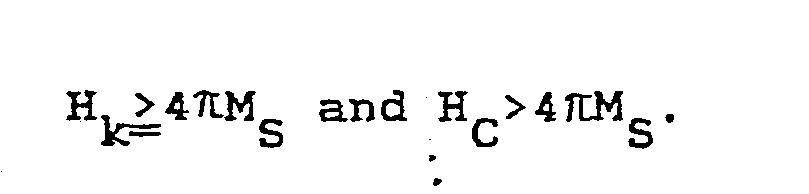
- the anisotropic magnetic field H K at right angles to the thin film plane of the magnetic materials, its coercive force He and its saturation magnetization 4 ⁇ M S should satisfy the relation H K ⁇ 4 ⁇ M S and H C >4 ⁇ M S .
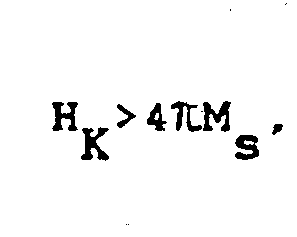
- the anisotropic magnetic field H K at right angles to the thin film plane of the magnetic materials and its saturation magnetization 4 ⁇ M S should satisfy the relation H k >4 ⁇ M S .
- Magnetic garnet expressed (for example) by the general formulae given below, is used as the magnetic materials. Magnetic materials fulfilling the conditions described above, and thus magnetic field sensors of the constructions (1) to (4) described above, can be obtained by altering its composition as appropriate.
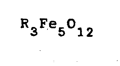
- the magnetic garnet used has the composition expressed by the ist general formula R 3 Fe 5 O 12 (where R is at least one element selected from Y, La, Ce, Nd, Pr, Sm, Eu, Gd, Tb, Dy, Ho, Er, Tm, Yb and Lu), the composition expressed by the 2nd general formula [Bi x R 3-x ]Fe 5 O 12 (where R is at least one element selected from Y, La, Ce, Nd, Pr, Sm, Eu, Gd, Tb, Dy, Ho, Er, Tm, Yb and Lu, 0.01 ⁇ x ⁇ 2.5), or the composition expressed by the 3rd general formula [Bi x R 3-x ](Fe 5-y-z M y N z )O 12 (where R is at least one element selected from Y, Ca, Sr, La, Ce, Nd, Pr, Sm, Eu, Gd, Tb, Dy, Ho, Er, Tm, Yb and Lu; M is at least one element selected from Ga, Al, Ge, Si,
- Bi(Bismuth) has the action of enhancing the magnetooptic effect and increasing the sensitivity of the magnetic field sensor.
- the reason why the range of x, which represents the Bi content, was set at 0.01 ⁇ x ⁇ 2.5 is that with x at less than 0.01 there is no observable increase in the magnetooptic effect, while with x at more than 2.5 it is difficult to grow the single crystal, or the yield is inferior, or else more faults occur in the single crystal, making it unsuitable for use.
- the M which in the 3rd general formula is substituted for part of the Fe(Iron) is a non-magnetic element which has the action of turning the easy axis of magnetization to the thin film plane by reducing the perpendicular magnetic anisotropism, or of facing it at right angles to the thin film plane by reducing the saturization magnetization.
- the reason why the range of y, which represents the M content, was set at 0.1 ⁇ y ⁇ 2.0 is that with y at less than 0.01 the effects mentioned were not obtained, while with y at more than 2.0 the magnetooptic effect is reduced.
- the N which in the 3rd general formula is similarly substituted for part of the Fe has the action of increasing magnetization in the thin film plane or at right angles to it, and makes it possible to measure higher magnetic fields.
- the reason why the range of z, which represents the N content, was set at 0.01 ⁇ z ⁇ 1.0 is that with z at less than 0.01 the effects mentioned are not obtained, while with z at more than 1.0 the magnetooptic effect is reduced.
- M Ga, Al, Ge, Si, V, Sb
- N Ti, Cr, Mn, Ni, Co, Zr, Hf. Sn, Mg, In, Ta, Nb, Sc
- cases of construction (1), (3) and (4) can be measure over a wide range of magnetic field with a high accuracy
- case of construction (2) can be measuring over a small condition of the magnetic field with a high sensitivity and a high accuracy.
- the magnetic garnet expressed by general formulas R3Fe5012, [Bi x R 3-x ]Fe 5 O 12 or [Bi x R 3-x )(Fe 5-y-z M y R z )O 12 can be given an angle of Faraday rotation which is constant over a wide range of temperatures, by adjusting the Gd, Tb and Dy content of R, the M content y and the N content z.
- the thickness of the magnetic garnet film used in the invention is determined with reference to transmittivity and the size of the angle of Faraday rotation.
- the thickness is usually 1-400pm, and preferably 4-100 ⁇ m; several films may be used, superimposed.
- the thickness is usually at least 10 ⁇ m, and preferably at least 40 ⁇ m; several films may be used, arrayed in the direction of transmission of the light.
- a thin sheet, of a maximum thickness of 5mm may be used in place of the thin film.
- several thin films of magnetic garnet are used, of different temperature characteristics Faraday rotation angle, with their composition adjusted as described above, performance can be obtained which is stable despite changes of temperature, enabling measurement to be made of magnetic fields over a wide range of temperatures.
- the magnetic garnet thin film used in the invention can be of any shape (circular, rectangular, etc.), and there is no need to adopt any specific shape.
- the ratio of thickness t to length (especially minimum length of the thin film or thin sheet is preferably t/l s ⁇ 0.5.
- the magnetic garnet used in the invention can be either single crystal or polycrystalline; but usually single crystal, which absorbs little light, is preferable.
- Common methods of growing such single crystals include the flux method process, which uses the oxides PbO, PbF 2 , Bi 2 0 3 , Mo03, V 0 etc. as flux, the CVD (Chemical Vapor Deposition) method, the LPE (Liquid Phase Epitaxial) method, the FZ (Floating zone) method, the TSSG (Top Seeded Solution Growth) method and the hydrothermal method.
- Anisotropy induced by uniaxial growth tends to occur in magnetic garnet single crystal grown by the LPE or flux methods, which are those most commonly used at the present time.
- magnetic garnet single crystal grown by the flux method for example, has uniaxial magnetic anisotropy
- the magnetic garnet thin film is prepared by cutting horizontally to the plane of the film in the direction in which the uniaxial magnetic anisotropy has developed (this is the easy axis of magnetization).
- the easy axis of magnetization and the direction of measuring magnetic field can provide at right angle to each other, for the magnetic field sensor of every constructions (1), (2), (3) and (4).
- the easy axis of magnetization is in any one of the directions ⁇ 111>, ⁇ 110> and ⁇ 100>.
- the uniaxial magnetic anisotropy energy K U can be change to maximum to about 10 5 erg/cm 3 by controlling the composition.
- M s can be prepere to the range of 0-160Gauss.
- H becomes to the value of maximum some 10KOe.
- large K U can be giving in which the composition elements containe Pr, Nd, Sm, Eu, Tb and Bi.
- gadolinium gallium garnet Gd 3 Ga 5 O 12 which has ⁇ 111 ⁇ faces is usually used as the substrate of the construction (3) or (4), and the thin film is formed by epitaxial growth on this substrate of the desired magnetic garnet single crystal.
- the easy axis of magnetization can be made to be in the thin film plane if the axis is in the ⁇ 1 10> direction. If the axis is in the ⁇ 111> or ⁇ 100> direction, it can similarly be made to be in the thin film plane by using ⁇ 110 ⁇ face substrate.
- the easy axis of magnetization of magnetic garnet and the direction of the magnetic field to be measured are perfectly coincided at right angles, but :f it does accuracy not at right angles, a object of the present invention may sufficiently achieve by changing relatively in the sensitivity of measurenent, and when increasing the sensitivity of measurement in the construction (2), it is desirable to reduce the uniaxial magnetic anisotropy.
- Fig. 1 is a block diagram of a magnetic field sensor according to the invention.
- a light source 11 a polarizer 12, a Faraday element 13 in the form of a thin film, a polarizer 14 and a photoreceptor element 15 are arranged in sequence. They are linked, by optical means such as optical fibres, lenses or the like (not shown in the drawing).
- the easy axis of magnetization of Faraday element 13 is in the thin film plane, and the thin film plane is arranged at right angles to the direction 16 of the magnetic field to be measured.
- the light is transmitted at right angles to the thin film ' plane of Faraday element 13.
- the arrangement is such that, as shown in Fig. 2, the beam of light 17 which passes through Faraday element 13 does not traverse the magnetic walls 18 of Faraday element 13.
- Fig. 3 is a block diagram of another magnetic field sensor according to the invention.
- a light source 21, a polarizer 22, a Faraday element 23 in the form of a thin film, a polarizer 24 and a photoreceptor 25 are arranged in sequence. They are linked, by optical means such as optical fibres, lenses or the like (not shown in the drawing).
- the thin film plane is parallel to the direction 26 of the magnetic field to be measured, so that the easy axis of magnetization of Faraday element 23 is unidirectional, at right angles to the thin film plane, and at right angles to the direction 26 of the magnetic field to be measured.
- the light is transmitted at right angles to the thin film plane of Faraday element 23.
- Fig. 4 is a block diagram of another magnetic field sensor according to the invention.
- a light source 31 a polarizer 32, a Faraday element 33 in the form of a thin film, a polarizer 34 and a photoreceptor 35 are arranged in sequence. They are linked, by optical means such as optical fibres, lenses or the like (not shown in the drawing).
- the thin film plane is parallel to the direction 36 of the magnetic field to be measured, so that the easy axis of magnetization of Faraday element 33 is at right angles to the thin film plane and to the direction 36 of the magnetic field to be measured.
- the light is transmitted parallel to the thin film plane of Faraday element 33.
- the incident light beam 37 which passes through Faraday element 33 can traverse the magnetic walls of Faraday element 33.
- Measurement of a magnetic field is effected by the magnetic field sensor shown in Fig. 4 on the same principle as in the case of the magnetic field sensor shown in Fig. 1.
- Fig. 6 is a block diagram of another magnetic field sensor according to the invention.
- a light source 41, a polarizer 42, a Faraday element 43 in the form of a thin film, a polarizer 44 and a photoreceptor 45 are arranged in sequence. They are linked, by optical means such as optical fibres, lenses or the like (not shown in the drawing).
- the thin film plane is parallel to the direction 46 of the magnetic field to be measured, so that the axis of easy magnetization of Faraday element 43 is in the thin film plane and at right angles to the direction 46 of the magnetic field to be measured.
- the light is transmitted parallel into the thin film plane of Faraday element 43.
- the polarizers were rutile Ti0 2 single crystal
- the photoreceptor was a photodiode (p-i-n PD) of InGaAs.
- the Faraday elements used consisted of the thin films of magnet garnet of Embodiments 1-19 having the composition shown in the Tables 1 and 2 below (Embodiment 1-4 for the magnetic field sensor of Fig. 1, Embodiments 5-9 for the magnetic field sensor of Fig. 3, Embodiments 10-14 for the magnetic field sensor of Fig. 4 and Embodiments 1 5-19 for the magnetic field sensor of Fig. 6). Changes in output P were investigated by applying magnetic fields to each Faraday element in the prescribed direction.
- Magnetic garnet thin films were made by being as follows.
- the magnetic garnet thin films of constructions of Embodiments 1-4 and 15-19 were grown by LPE method or flux method and cutting to parallel to the direction of the single axis of anisotropic magnetic on a Gd 3 Ga 5 O 12 , Nd 3 Ga 5 O 12 or (GdCa) 3 (MgZrGa) 5 O 12 single crystal substrate'as it becomes to ⁇ 110 ⁇ plane or ⁇ 111 ⁇ plane in the thin film plane'for the easy magnetized axis of thickness 0.5mm.
- the magnetic garnet thin films of constructions of Embodiments 5-14 were grown by LPE method or flux method and cutting at right angle to the direction of the single axis of anisotropic magnetic on a Gd 3 Ga 5 O 12 , Nd 3 Ga 5 O 12 or (GdCa) 3 (MgZrGa) 5 O 12 single crystal substrate as it becomes to ⁇ 111 ⁇ plane at right angle on the thin film plane for the easy magnetized axis of thickness 0.5mm.
- the thickness of the thin film of magnetic garnet was, for example, 40 ⁇ m-400 ⁇ m in the case of the magnetic garnet thin film of Embodiment 1-9, and 200pm-700pm in that of the thin film of Embodiment 10-19.
- Fig. 8 shows the relation between the applied magnetic field and the angle of Faraday rotation, for Embodiments 1, 4 and 10 and Examples 1 and 2 for Comparison; and Fig. 9, the relation between the magnetic field applied and the angle of Faraday rotation for Embodiment 15 and Example 4 for Comparison.
- the magnetic field sensor of the Embodiments 1-14 of the present invention appears a high output power and an exelent resolution (resolving power), and it is clear that the magnetic field sensor of Embodiments 1-14 has a very widly measring range of magnetic field than each magnetic field sensor of comparison Examples 1-3. And, the magnetic field sensor of Embodiments 15-19 have a high measuring sensitivity than comparisons.
- the construction and the magnetic materials of the magnetic field sensor according to the invention can be utilize as a magnetic field sensor used with the optical heterodyne phase detector (Japanese Patent Disclosure Nos. 59-19875, 59-52774), which the magnetic field measurement having the high sensitivity is possible.
- Fig. 10 shows four curves relation to the angle of Faraday rotation for the temperature of the magentooptic element 13.
Landscapes
- Engineering & Computer Science (AREA)
- Power Engineering (AREA)
- Physics & Mathematics (AREA)
- Condensed Matter Physics & Semiconductors (AREA)
- General Physics & Mathematics (AREA)
- Measuring Magnetic Variables (AREA)
Abstract
Description
- This invention relates to a magnetic field sensor which uses the magneto-optic effect of a magnetic material. In particular, it provides a magnetic field sensor which can measure a wide range of magnetic fields with a high degree of accuracy.
- In the field of electric power, the efficient running and automation of electric power systems of increasing capacity necessitate digital control and protection systems for high voltage plate in substations and the like. Current and voltage sensors for controlling and measuring the current and voltage of high-voltage power transmitters and transformers are indispensable for this purpose. The need for the equipment to be small, low-cost and reliable means that current and voltage sensors must be well insulated against high voltages, resistant to electro-magnetic faults, miniaturised, and of high performance.
- Hitherto, control and measurement of current has been effected by using a. large transformer with a core and windings, but this means that there is a space problem and there are problems related to poor insulation against high voltage and poor resistance to electro-magnetic noise.
- In order to solve the problems associated with transformers described, the optical magnetic field sensor has been developed as a current sensing device for electrical systems. In recent years, magnetic garnet single crystal and ZnSe single crystal having a large magneto-optic effect (Faraday effect) and little optical absorption have been disclosed in reports of optical magnetic field sensors which use these in combination with optical fibres (e.g. National Technical Report, Vol. 29, No. 5, Oct. 1983, pp 70-80; Keiso, Vol. 26, No. 11, Oct. 1983, pp 56-60 and Japanese Patent Disclosure No. 58-139082).
- These optical magnetic field sensors consist of a light source part (e.g. a light-emitting diode), a magnetic field detection part, containing magnetic garnet single crystal having a Faraday effect (e.g. (Y-Tb)3Fe5O12, (Y-Sm-Lu-Ca)3(Fe-Ge)5O12, [Y0.3Sm0.5Lu1.4Ca0.6Gd0.2](Fe4.4Ge0.6)O12) and polarizer, a light-measuring part which receives and measures the light which is radiated from the light source part and passes through the magnetic field detection part, and an optical transmission line which links by optical means the light source part, magnetic field detection part and light-measuring part.
- As shown in Figure 7 of the accompanying drawings which is a block diagram of a conventional magnetic field sensor, there is a
light source 1, apolarizer 2, a Faraday element (magnetic garnet in the form of a thin film) 3 as a magneto-optical element, apolarizer 4 and a photo-receptor element 5, arranged in sequence. They are linked, by optical means for light transmission, such as optical fibres, lenses or the like (not shown). The direction of the axis of easy magnetization of Faradayelement 3 is at right angles to the thin film plane, and maze-like magnetic domains are formed in the thin film. This Faradayelement 3 has the thin film element disposed at right angles toL'he direction 6 of the magnetic field to be measured, so that its axis of easy magnetization is parallel to the direction of the magnetic field to be measured (Japanese Patent Disclosure Nos. 58-139082, 58-27071, 58-27072). The light is transmitted at right angles to the thin film plane of Faradayelement 3.Polarizers - The principle of this optical magnetic field sensor will now be explained. The light radiated from
light source 1 first becomes polarized light atpolarizer 2, then passes through Faradayelement 3. When the magnetic field applied to Faradayelements 3 is 0 (zero), Faradayelement 3 is in a demagnetized state and, since there is no magnetization component in the direction of transmission of the light, the plane of polarization of the light does not rotate. As the axes of polarization betweenpolarizers light source 1 is detected byphotoreceptor element 5. In this case, the light is reduced only by the amount of attenuation in the members constituting the sensor. - When on the other hand a magnetic field H is applied to Faraday
element 3, the magnetic field H induces a magnetization component in Faradayelement 3 in the direction of transmission of the light, and the plane of polarization of the linearly polarized light passing throughFaraday element 3 is rotated through an angle θ proportionate to M, namely

polarizer 4 and detected by thephotoreceptor element 5. In the magnetic field sensor described above, therefore, the size of magnetic field H is measured by the change in light intensity P. - However, the arrangement of this kind of magnetic field sensor, in which the direction of the axis of ease of magnetization of the magnetic garnet single crystal in the form of a thin film is at right angles to the thin film plane, maze-like magnetic domains are formed in the film plane, the axis of easy magnetization of the magnetic garnet single crystal is parallel to the direction of the magnetic field to be measured, and the magnetic field is measured by the changes in magnetization produced by movements of the walls of the domains, gives rise to the following problems. If the diameter of the beam of light is small, it is liable to be affected by non-uniformity of the pattern width of the magnetic domains, and by the width of these domains. This means that if the magnetic field to be measured changes dynamically, the.angle g may also change, depending on the shape and direction of the magnetic garnet single crystals, in relation to the same magnetic field being measured. This makes it difficult to measure the magnetic field with a high degree of accuracy. A further problem is that since, if the saturation magnetization is large, the energy of the demagnetizing field is also increased, the saturation magnetization can not, in general, be permitted to be large, with the result that it is difficult to measure a high magnetic field.
- Non-magnetic ZnSe can be used in place of magnetic garnet single crystal when measuring a high magnetic field. But there is a problem here too, in the ZnSe has only a small magnetooptic effect and low sensitivity.
- In addition to the above mentioned problems that is liable to affected by the width of the magnetic domains, the conventional optical magnetic field sensor is a difficulty to measure for the small magnetic field having the limitation by the saturation magnetization Ms. Because, the measurement sensitivity S with M is expressed in the cause of the magnetized directin or the shape of the magnetic garnet single crystals to be used as Faraday elements;

- It is object of the present invention to provide a magnetic field sensor which can measure a wide range of Magnetic fields with a high output power signal and with a high degree of accuracy.
- To accomplish the objects of the present invention, provides with a light source part, a magnetic field detection part which contains a magnetooptic element consisting of a magnetic materials having a magnetooptic effect, and a light measurement part which measures the light that has been radiated from the light source part and has passed through the magnetic field detection part, is characterized in that the magnetooptic element is arranged such that its axis of easy magnetization is at right angles to the direction of the magnetic field to be measured.
- The following may be cited as specific_examples of the construction of the magnetic field sensor of the invention: (1) a construction in which the magnetooptic element is in the form of a thin film, with its axis of easy magnetization in the thin film plane, that is, the direction of the easy magnetization axis is parallel to'the thin film plane, the thin film plane of the magnetooptic element is at right angles to the direction of the magnetic field to be measured, and the light is transmitted at right angles to the thin film plane, that is , a direction of the incident light beam is at right angles to the thin film plane; (2) a construction in which the magnetooptic elemtn is in the form of a thin film, with its axis of easy magnetization in the thin film plane, the thin film plane of the magnetooptic element is parallel to the direction of the magnetic field to be measured, and the light is transmitted parallel to the thin film plane; (3) a construction in which the magnetooptic element is in the form of a thin film, with its axis of easy magnetization facing in one direction, at right angles to the thin film plane, the thin film plane of the magnetooptic element is parallel to the direction of the magnetic field to be measured, and the light is transmitted at right angles to the thin film plane of the magnetooptic element; or (3) a construction in which the magnetooptic element is in the form of a thin film, with its axis of easy magnetization at right angles-to the thin film plane, the thin film plane of the magnetooptic element is parallel to the direction of the magnetic field to be measured, and the light is transmitted parallel to the thin film plane of the magnetooptic element.
- The magnetic materials which is used in above mentioned cases (1), (2), (3) and (4) is preferably constituted the magnetooptic element has uniaxial magnetic anisotropy.
- When the axis of easy magnetization of the magnetic materials is in the thin film plane, as in constructions (1) or (2), the anisotropic magnetic field H of the magnetic ' materials constituting the magnetooptic element, at right angles to its thin film planes, and its saturation magnetization 4πMS should satisfy the relation HK<4πMS. When the axis of easy magnetization of the magnetic materials faces in one direction, at right angles to the thin film plane, as in construction (3), the anisotropic magnetic field H K at right angles to the thin film plane of the magnetic materials, its coercive force He and its saturation magnetization 4πMS should satisfy the relation HK≧4πMS and HC>4πMS. When the axis of easy magnetization of the magnetic materials is at right angles to the thin film plane, as in constructin (4), the anisotropic magnetic field HK at right angles to the thin film plane of the magnetic materials and its saturation magnetization 4πMS should satisfy the relation Hk>4πMS.
- Magnetic garnet, expressed (for example) by the general formulae given below, is used as the magnetic materials. Magnetic materials fulfilling the conditions described above, and thus magnetic field sensors of the constructions (1) to (4) described above, can be obtained by altering its composition as appropriate.
- The magnetic garnet used has the composition expressed by the ist general formula R3Fe5O12 (where R is at least one element selected from Y, La, Ce, Nd, Pr, Sm, Eu, Gd, Tb, Dy, Ho, Er, Tm, Yb and Lu), the composition expressed by the 2nd general formula [BixR3-x]Fe5O12 (where R is at least one element selected from Y, La, Ce, Nd, Pr, Sm, Eu, Gd, Tb, Dy, Ho, Er, Tm, Yb and Lu, 0.01≦x≦2.5), or the composition expressed by the 3rd general formula [BixR3-x](Fe5-y-zMyNz)O12 (where R is at least one element selected from Y, Ca, Sr, La, Ce, Nd, Pr, Sm, Eu, Gd, Tb, Dy, Ho, Er, Tm, Yb and Lu; M is at least one element selected from Ga, Al, Ge, Si, V and Sb, and N is at least one element selected from Ti, Cr, Mn, Ni, Co, Zr, Hf, Sn, Mg, In, Ta, Nb and Sc, 0.01≤x≤2.5, 0.01≤y≤2.0, 0.01≤z≤1.0).
- - An explanation follows of the action of the elements constituting the magnetic garnet expressed by these formula, and of the reasons for the limits set to their contents in each case.
- Bi(Bismuth) has the action of enhancing the magnetooptic effect and increasing the sensitivity of the magnetic field sensor. The reason why the range of x, which represents the Bi content, was set at 0.01≤x≤2.5 is that with x at less than 0.01 there is no observable increase in the magnetooptic effect, while with x at more than 2.5 it is difficult to grow the single crystal, or the yield is inferior, or else more faults occur in the single crystal, making it unsuitable for use.
- The M which in the 3rd general formula is substituted for part of the Fe(Iron) is a non-magnetic element which has the action of turning the easy axis of magnetization to the thin film plane by reducing the perpendicular magnetic anisotropism, or of facing it at right angles to the thin film plane by reducing the saturization magnetization. The reason why the range of y, which represents the M content, was set at 0.1<y<2.0 is that with y at less than 0.01 the effects mentioned were not obtained, while with y at more than 2.0 the magnetooptic effect is reduced.
- The N which in the 3rd general formula is similarly substituted for part of the Fe has the action of increasing magnetization in the thin film plane or at right angles to it, and makes it possible to measure higher magnetic fields. The reason why the range of z, which represents the N content, was set at 0.01≤z≤1.0 is that with z at less than 0.01 the effects mentioned are not obtained, while with z at more than 1.0 the magnetooptic effect is reduced.
- Because it contains Bi, magnetic garnet expressed by the general formulae given above has a very large magnetooptic effect and outstanding magnetic field sensitivity, and thus can measure minute magnetic fields. The M (Ga, Al, Ge, Si, V, Sb) and N (Ti, Cr, Mn, Ni, Co, Zr, Hf. Sn, Mg, In, Ta, Nb, Sc) components enable it, moreover, to measure high magnetic fields. Among the N components, ..his effect is particularly marked in the case of Co(Cobalt).
- By selecting the suitable composition, above mentioned cases of construction (1), (3) and (4) can be measure over a wide range of magnetic field with a high accuracy, and the case of construction (2) can be measuring over a small condition of the magnetic field with a high sensitivity and a high accuracy.
- Furthermore, in this invention the magnetic garnet expressed by general formulas R3Fe5012, [BixR3-x]Fe5O12 or [BixR3-x)(Fe5-y-zMyRz)O12 can be given an angle of Faraday rotation which is constant over a wide range of temperatures, by adjusting the Gd, Tb and Dy content of R, the M content y and the N content z.
- The thickness of the magnetic garnet film used in the invention is determined with reference to transmittivity and the size of the angle of Faraday rotation. When the light is transmitted at right angles to the thin film plane of the magnetic materials, as in magnetic field sensors of constructions (1) or (3), the thickness is usually 1-400pm, and preferably 4-100µm; several films may be used, superimposed. When the light is transmitted parallel to the thin film plane of the magnetic materials, as in a magnetic field sensor of construction (2) or (4), the thickness is usually at least 10µm, and preferably at least 40µm; several films may be used, arrayed in the direction of transmission of the light. Alternatively, a thin sheet, of a maximum thickness of 5mm, may be used in place of the thin film. In particular, if several thin films of magnetic garnet are used, of different temperature characteristics Faraday rotation angle, with their composition adjusted as described above, performance can be obtained which is stable despite changes of temperature, enabling measurement to be made of magnetic fields over a wide range of temperatures.
- The magnetic garnet thin film used in the invention can be of any shape (circular, rectangular, etc.), and there is no need to adopt any specific shape. The ratio of thickness t to length (especially minimum length of the thin film or thin sheet is preferably t/ℓs≦0.5.
- The magnetic garnet used in the invention can be either single crystal or polycrystalline; but usually single crystal, which absorbs little light, is preferable. Common methods of growing such single crystals include the flux method process, which uses the oxides PbO, PbF2,
Bi 203, Mo03,V 0 etc. as flux, the CVD (Chemical Vapor Deposition) method, the LPE (Liquid Phase Epitaxial) method, the FZ (Floating zone) method, the TSSG (Top Seeded Solution Growth) method and the hydrothermal method. - Anisotropy induced by uniaxial growth (uniaxial magnetic anisotropy) tends to occur in magnetic garnet single crystal grown by the LPE or flux methods, which are those most commonly used at the present time.
- When magnetic garnet single crystal grown by the flux method, for example, has uniaxial magnetic anisotropy, it can be used in the magnetic field sensors of constructions (1) and (2), the magnetic garnet thin film is prepared by cutting horizontally to the plane of the film in the direction in which the uniaxial magnetic anisotropy has developed (this is the easy axis of magnetization). And magnetic garnet single crystal which can be used in the magnetic field sensors of constructions (3) or (4) if the magnetic garnet thin film is prepared by cutting vertically in the direction in which the uniaxial magnetic anisotropy has developed. Such as if the magnetic garnet thin film is prepared by cutting horizontally or vertically in the direction in which the uniaxil magnetic anisotropy has developed, the easy axis of magnetization and the direction of measuring magnetic field can provide at right angle to each other, for the magnetic field sensor of every constructions (1), (2), (3) and (4).
- In magnetic garnet single crystal thin film, the easy axis of magnetization, while it also depends on the composition, is in any one of the directions <111>, <110> and <100>. In the magnetic field sensor of constructions (1), (2), (3) and (4) having such uniaxial magnetic anisotropy, because the change of magnetization occures by the rotation of magnetic moment, the limit of the magnetic field H that can be measured is the sum of the s demagnetizing field (N·41πMs) and the anisotropic magnetic field Hk (=2KU/MS). This makes it possible to measure high magnetic fields.
- Namely, the uniaxial magnetic anisotropy energy KU can be change to maximum to about 105erg/cm3 by controlling the composition. Ms can be prepere to the range of 0-160Gauss. H becomes to the value of maximum some 10KOe. And then the s measurement of the high magnetic field is possible. paticuraly, large KU can be giving in which the composition elements containe Pr, Nd, Sm, Eu, Tb and Bi. And in the magnetic field sensor of the construction (2), the limit of the magnetic field Hs can be to small than Ms, because the affection of the demagnetizing is not but the change of the magnetization lieses by magnetic rotations, and measuring sensitivity S (S=θF·ℓ/Hs) becomes to large, because of the measurement of the high sensitivity and high accuracy for small magnetic field becomes to possible.
- In the LPE method, gadolinium gallium garnet Gd3Ga5O12 (GGG) which has {111} faces is usually used as the substrate of the construction (3) or (4), and the thin film is formed by epitaxial growth on this substrate of the desired magnetic garnet single crystal. In the case of the substrate of the construction (1) or (2), the easy axis of magnetization can be made to be in the thin film plane if the axis is in the <110> direction. If the axis is in the <111> or <100> direction, it can similarly be made to be in the thin film plane by using {110} face substrate.
- When growing magnetic garnet single crystal with e.g. a high Bi content, it is preferable to use a single crystal substrate of Nd 3 Ga 5 0 12' Sm3Ga5012 or their derivatives, in which there is minimal mismatch of lattice constants with the magnetic garnet single crystal, in place of the GGG substrate.
- With the magnetic field sensor according to the present invention, it is desirable, the easy axis of magnetization of magnetic garnet and the direction of the magnetic field to be measured are perfectly coincided at right angles, but :f it does accuracy not at right angles, a object of the present invention may sufficiently achieve by changing relatively in the sensitivity of measurenent, and when increasing the sensitivity of measurement in the construction (2), it is desirable to reduce the uniaxial magnetic anisotropy.
- It is further desirable, when necessary to control the magnitude of the uniaxis magnetic absotropy in the construction (1) and using a specific orientation plane of magnetic garnet crystal, to reduce the uniaxial magnetic anisotropy that is produced at right angles to that plane. With magnetic garnet single crystal which has uniaxial anisotropy at right angles to the thin film plane, this uniaxial magnetic anisotropy can be reduced, and the direction of magnetization made to lie in the thin film plane, by annealing. The temperature of this annealing is preferably 900-1500°C. This is because if the annealing temperature is lower than 900°C there is no observable reduction of uniaxial magnetic anisotropy, while if it exceeds 1500°C the light absorption coefficient increases, with a consequent reduction in the sensitivity of the magnetic field sensor.
- With a magnetic field sensor of this kind, since the easy axis of magnetization of the magnetooptic element (Faraday element) is at right angles to the direction of the magnetic field to be measured, the magnetization component in the direction of the magnetic field to be measured is -produced by a mechanism of the magnetic rotation magnetic and this magnetization component changes linearly in proportion to the size of the magnetic field to be measured, right up to high magnetic fields. Again, since the effect of non-uniformity of the pattern of the magnetic domains, and of the width of the magnetic domains, can be avoided, not only when the magnetooptic element does not form maze-like magnetic domains, but even when it does form such domains, magnetic fields can be measured with a high degree of accuracy.
-
- Fig. 1 is a block diagram of a optical magnetic field sensor according to the invention.
- Fig. 2 shows the ralation of directions of, the incident light beam which passes through Faraday element, the magnetic field to be measured and the easy axis of magnetization.
- Fig. 3, Fig. 4 and Fig. 5 are a block diagram of a magnetic field sensor according to another embodiment of the invention, respectively.
- Fig. 6 shows the ralation of directions of, the incident light beam which passes through Faraday element, the magnetic field to be measured and the easy axis of magnetization, of another embodiment.
- Fig. 7 is a block diagram of the conventional magnetic field sensor.
- Fig. 8 and Fig. 9 show the characteristics for embodiments and comparisons, respectively.
- Fig. 10 shows the characteristics for temperature of the superimporsed construction according to the invention.
- Embodiments of the invention are explained below, referring to the drawings.
- Fig. 1 is a block diagram of a magnetic field sensor according to the invention. In this drawing, a
light source 11, apolarizer 12, aFaraday element 13 in the form of a thin film, apolarizer 14 and aphotoreceptor element 15 are arranged in sequence. They are linked, by optical means such as optical fibres, lenses or the like (not shown in the drawing). - In this magnetic field sensor, the easy axis of magnetization of
Faraday element 13 is in the thin film plane, and the thin film plane is arranged at right angles to thedirection 16 of the magnetic field to be measured. The light is transmitted at right angles to the thin film ' plane ofFaraday element 13. - The arrangement is such that, as shown in Fig. 2, the beam of light 17 which passes through
Faraday element 13 does not traverse themagnetic walls 18 ofFaraday element 13. Polarizers 12 and 14 are disposed such that the axis of polarization between them is rotated through an angle of 45°. Signal-processing is carried out to ensure that when the magnetic field to be measured H=0, the output signal P=O. - The principle of this magnetic field sensor will now be explained. First, the light radiated from
light source 11 passes via optical fibres (not shown in the drawing) throughpolarizer 12, becoming linearly polarized light. Next, this linearly polarized light strikes, at right angles, the thin film plane ofFaraday element 13. When magnetic field to be measured H is applied toFaraday element 13, magnetization M is produced in the transmission direction of the light, in proportion to the magnetic field, and after the linearly polarized light has passed throughFaraday element 13, the angle θ of inclination of its plane of polarization is rotated in proportion to this magnetization by an amount θ=θF·ℓ·M/MS (where θF: coefficient of Faraday rotation, ℓ: optical path of Faraday element, MS: saturation magnetization of magnetic garnet). Its plane of polarization having been rotated through the angler, the linearly polarized light passes throughpolarizer 14 and is directed via optical fibres tophotoreceptor 15, to obtain output signal P. Thus magnetic field H is measured as output signal P. - Fig. 3 is a block diagram of another magnetic field sensor according to the invention. In this drawing, a
light source 21, apolarizer 22, aFaraday element 23 in the form of a thin film, apolarizer 24 and aphotoreceptor 25 are arranged in sequence. They are linked, by optical means such as optical fibres, lenses or the like (not shown in the drawing). - In this magnetic field sensor, the thin film plane is parallel to the
direction 26 of the magnetic field to be measured, so that the easy axis of magnetization ofFaraday element 23 is unidirectional, at right angles to the thin film plane, and at right angles to thedirection 26 of the magnetic field to be measured. The light is transmitted at right angles to the thin film plane ofFaraday element 23. - Polarizers 22 and 24 are disposed such that the axis of polarization between them is rotated through an angle of 45°. Single-processing is carried out to ensure that when the magnetic field to be measured H=0, the output signal P=O. Measurement of a magnetic field is effected by the magnetic field sensor shown in Fig. 3 on the same principle as in the case of the magnetic field sensor shown in Fig. 1.
- Fig. 4 is a block diagram of another magnetic field sensor according to the invention. In this drawing, a
light source 31, apolarizer 32, aFaraday element 33 in the form of a thin film, apolarizer 34 and aphotoreceptor 35 are arranged in sequence. They are linked, by optical means such as optical fibres, lenses or the like (not shown in the drawing). - In this magnetic field sensor, the thin film plane is parallel to the
direction 36 of the magnetic field to be measured, so that the easy axis of magnetization ofFaraday element 33 is at right angles to the thin film plane and to thedirection 36 of the magnetic field to be measured. The light is transmitted parallel to the thin film plane ofFaraday element 33. - As shown in Fig. 5, the
incident light beam 37 which passes throughFaraday element 33 can traverse the magnetic walls ofFaraday element 33. Polarizers 32 and 34 are disposed such that the axis of polarization between them is rotated through an angle of 45°. Single-processing is carried out to ensure that when the magnetic field to be measured H=O, the output signal P=0. - Measurement of a magnetic field is effected by the magnetic field sensor shown in Fig. 4 on the same principle as in the case of the magnetic field sensor shown in Fig. 1.
- Fig. 6 is a block diagram of another magnetic field sensor according to the invention. In this drawing, a
light source 41, apolarizer 42, aFaraday element 43 in the form of a thin film, apolarizer 44 and aphotoreceptor 45 are arranged in sequence. They are linked, by optical means such as optical fibres, lenses or the like (not shown in the drawing). - In this magnetic field sensor, the thin film plane is parallel to the
direction 46 of the magnetic field to be measured, so that the axis of easy magnetization ofFaraday element 43 is in the thin film plane and at right angles to thedirection 46 of the magnetic field to be measured. The light is transmitted parallel into the thin film plane ofFaraday element 43. - Polarizers 42 and 44 are disposed such that the axis of polarization between them is rotated through an angle of 45. Single-processing is carried out to ensure that when the -magnetic field to be measured H=0, the output signal P=0. Measurement of a magnetic field is effected by the magnetic field sensor shown in Fig. 6 on the same principle as in the case of the magnetic field sensor shown in Fig. 1.
- In the magnetic field sensors shown above, the light source used was an LED of wavelength X = 1.3µm, the polarizers were rutile Ti02 single crystal, and the photoreceptor was a photodiode (p-i-n PD) of InGaAs. The Faraday elements used consisted of the thin films of magnet garnet of Embodiments 1-19 having the composition shown in the Tables 1 and 2 below (Embodiment 1-4 for the magnetic field sensor of Fig. 1, Embodiments 5-9 for the magnetic field sensor of Fig. 3, Embodiments 10-14 for the magnetic field sensor of Fig. 4 and Embodiments 15-19 for the magnetic field sensor of Fig. 6). Changes in output P were investigated by applying magnetic fields to each Faraday element in the prescribed direction.
- These magnetic garnet thin films were made by being as follows. The magnetic garnet thin films of constructions of Embodiments 1-4 and 15-19 were grown by LPE method or flux method and cutting to parallel to the direction of the single axis of anisotropic magnetic on a Gd3Ga5O12, Nd3Ga5O12 or (GdCa)3(MgZrGa)5O12 single crystal substrate'as it becomes to {110} plane or {111} plane in the thin film plane'for the easy magnetized axis of thickness 0.5mm. The magnetic garnet thin films of constructions of Embodiments 5-14 were grown by LPE method or flux method and cutting at right angle to the direction of the single axis of anisotropic magnetic on a Gd3Ga5O12, Nd3Ga5O12 or (GdCa)3(MgZrGa)5O12 single crystal substrate as it becomes to {111} plane at right angle on the thin film plane for the easy magnetized axis of thickness 0.5mm.
- The thickness of the thin film of magnetic garnet was, for example, 40µm-400µm in the case of the magnetic garnet thin film of Embodiment 1-9, and 200pm-700pm in that of the thin film of Embodiment 10-19.
- Conventional magnetic field sensors (Fig. 7), with a Faraday element consisting of non-magnetic ZnSe single crystal (film thickness 5mm) such as has been mentioned in the published reports (Example 1 for Comparison), and of magnetic garnet thin film of the compositions listed in the Table below (Examples 2, 3 and 4 for Comparison) (film thickness 100µm, 100µm and 500µm, respectively), were prepared for comparison with the magnetic field sensors described above, and measurement carried out in the manner described.
- The Tables 1 and 2 below summarize the output, resolving power and range of magnetic field measured, of the various magnetic field sensors. Fig. 8 shows the relation between the applied magnetic field and the angle of Faraday rotation, for
Embodiments Embodiment 15 and Example 4 for Comparison.
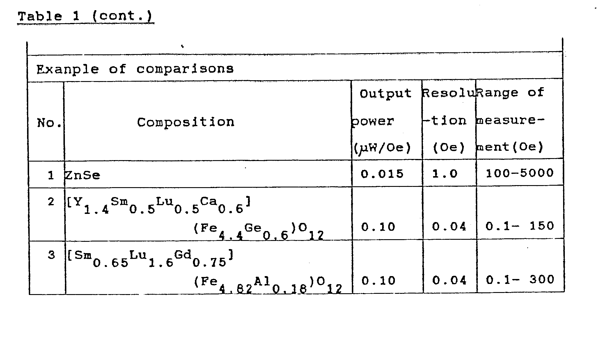

- As is evident from Tables 1 and 2 that the magnetic field sensor of the Embodiments 1-14 of the present invention appears a high output power and an exelent resolution (resolving power), and it is clear that the magnetic field sensor of Embodiments 1-14 has a very widly measring range of magnetic field than each magnetic field sensor of comparison Examples 1-3. And, the magnetic field sensor of Embodiments 15-19 have a high measuring sensitivity than comparisons.
- And more, it is obvious that the Faraday rotation changes linearly until the maximum magnetic field to be measured for the applied magnetic field of on the plotted curves for the magnetic field sensor of Embodiments (1), (2), (10) and (15) as shown in Fig. 8 and Fig. 9.
- Still more, the same results was obtained by the thin film monocrystal (thickness 0.2-Imm) which grown with used the flux method.
- And still more, the construction and the magnetic materials of the magnetic field sensor according to the invention can be utilize as a magnetic field sensor used with the optical heterodyne phase detector (Japanese Patent Disclosure Nos. 59-19875, 59-52774), which the magnetic field measurement having the high sensitivity is possible.
- Fig. 10 shows four curves relation to the angle of Faraday rotation for the temperature of the
magentooptic element 13. - One curve is appeared the caracteristics indicated as Superimposed Construction Mode which is obtained by the
magnetooptic element 13 which is constructed in layers of several thin films of magnetic garnet such as G1: {Gd1.8(Y,Tb)1.2}Fe5O12, G2: (Gd1.0(Y,Tb)2.0)Fe5O12 and G3: {Gd0.3(Y,Tb)2.7}Fe5O12, parformanee can be obtained which is stable despite changes of temperature, enabling measurement to be made of magnetic fields over a wide range of temperature. And, other three curves are indicated with characteristics according to each magentic garnet of different types as Gl, G2 and G3.
Claims (16)


Applications Claiming Priority (6)
| Application Number | Priority Date | Filing Date | Title |
|---|---|---|---|
| JP14373285 | 1985-06-29 | ||
| JP143732/85 | 1985-06-29 | ||
| JP168944/85 | 1985-07-31 | ||
| JP16894485 | 1985-07-31 | ||
| JP266948/85 | 1985-11-27 | ||
| JP26694885 | 1985-11-27 |
Publications (3)
| Publication Number | Publication Date |
|---|---|
| EP0208476A2 true EP0208476A2 (en) | 1987-01-14 |
| EP0208476A3 EP0208476A3 (en) | 1987-08-19 |
| EP0208476B1 EP0208476B1 (en) | 1993-01-20 |
Family
ID=27318709
Family Applications (1)
| Application Number | Title | Priority Date | Filing Date |
|---|---|---|---|
| EP86304959A Expired - Lifetime EP0208476B1 (en) | 1985-06-29 | 1986-06-26 | Magnetic field sensor having magneto-optic element |
Country Status (4)
| Country | Link |
|---|---|
| US (1) | US4896103A (en) |
| EP (1) | EP0208476B1 (en) |
| JP (1) | JPH0766044B2 (en) |
| DE (1) | DE3687548T2 (en) |
Cited By (14)
| Publication number | Priority date | Publication date | Assignee | Title |
|---|---|---|---|---|
| EP0353057A3 (en) * | 1988-07-28 | 1990-03-28 | Ngk Insulators, Ltd. | Optical component and magnetic-field sensor using superposed single crystal elements having different optical properties |
| DE4027049A1 (en) * | 1989-09-07 | 1991-03-21 | Siemens Ag | METHOD FOR CHECKING CURRENT PATHS IN AN ELECTRONIC OR ELECTRICAL COMPONENT AND DEVICE FOR IMPLEMENTING THE METHOD |
| EP0501726A3 (en) * | 1991-03-01 | 1992-09-16 | Teijin Seiki Company Limited | Magnetic-field measuring apparatus |
| EP0510621A3 (en) * | 1991-04-25 | 1993-12-08 | Matsushita Electric Industrial Co Ltd | Magneto-optical element and magnetic field measurement apparatus |
| EP0565085A3 (en) * | 1992-04-10 | 1994-06-15 | Mitsubishi Gas Chemical Co | Magnetic field sensor |
| EP0573007A3 (en) * | 1992-06-03 | 1994-06-15 | Mitsubishi Gas Chemical Co | Magneto-optic sensor head |
| EP0415668B1 (en) * | 1989-08-29 | 1995-03-22 | Ngk Insulators, Ltd. | High sensitivity optical magnetic field sensors |
| EP0604721A3 (en) * | 1992-10-30 | 1995-03-29 | Ibm | Magneto-optic probe. |
| EP1806755A1 (en) * | 2006-01-10 | 2007-07-11 | TDK Corporation | Magnetic garnet single crystal and method for producing the same as well as optical element using the same |
| US7758766B2 (en) | 2007-09-17 | 2010-07-20 | Tdk Corporation | Magnetic garnet single crystal and Faraday rotator using the same |
| US7811465B2 (en) | 2004-11-19 | 2010-10-12 | Tdk Corporation | Magnetic garnet single crystal and optical element using same as well as method of producing single crystal |
| US7828895B2 (en) | 2006-01-27 | 2010-11-09 | Tdk Corporation | Method of producing optical element |
| US8142676B2 (en) | 2006-02-20 | 2012-03-27 | Tdk Corporation | Magnetic garnet single crystal and optical element using the same |
| CN104360152A (en) * | 2014-11-13 | 2015-02-18 | 北京航空航天大学 | Microwave sensor based on NV color center diamond |
Families Citing this family (26)
| Publication number | Priority date | Publication date | Assignee | Title |
|---|---|---|---|---|
| JPS62150185A (en) * | 1985-12-24 | 1987-07-04 | Matsushita Electric Ind Co Ltd | Magnetic field measuring device |
| US4952014A (en) * | 1987-10-19 | 1990-08-28 | At&T Bell Laboratories | Optical systems with thin film polarization rotators and method for fabricating such rotators |
| JPH0766114B2 (en) * | 1988-11-11 | 1995-07-19 | 富士電気化学株式会社 | Magneto-optical element material |
| IT1248820B (en) * | 1990-05-25 | 1995-01-30 | Pirelli Cavi Spa | FIELD DIRECTIONAL POLARIMETRIC SENSOR |
| US5640516A (en) * | 1991-04-02 | 1997-06-17 | Tdk Corporation | Faraday rotator |
| US5192862A (en) * | 1991-12-19 | 1993-03-09 | Simmonds Precision Products, Inc. | Polarizerless magneto-optic speed and torque sensor |
| US5412469A (en) * | 1992-11-16 | 1995-05-02 | Simmonds Precision Products, Inc. | Optical spectrum analyzer and encoder using a modulated phase grating wherein said grating diffracts the wavelength as a function of the magnetic field |
| US5493220A (en) * | 1993-03-05 | 1996-02-20 | Northeastern University | Magneto-optic Kerr effect stress sensing system |
| US5631559A (en) * | 1993-03-05 | 1997-05-20 | Northeastern University | Method and apparatus for performing magnetic field measurements using magneto-optic kerr effect sensors |
| US5994898A (en) * | 1993-03-05 | 1999-11-30 | Northeastern University | Apparatus and method for measuring instantaneous power using a magneto-optic Kerr effect sensor |
| US5757538A (en) * | 1995-02-16 | 1998-05-26 | Tokin Corporation | Optical isolator |
| JPH08306531A (en) * | 1995-05-10 | 1996-11-22 | Murata Mfg Co Ltd | Magnetostatic wave device |
| US5801875A (en) * | 1995-07-05 | 1998-09-01 | Lucent Technologies Inc. | Article comprising a magneto-optic material having low magnetic moment |
| JP3388319B2 (en) * | 1996-05-31 | 2003-03-17 | レンセレー ポリテクニク インスティテュート | Electro-optical and magneto-optical sensing devices and methods for characterizing free space electromagnetic radiation |
| JP3493119B2 (en) * | 1997-08-25 | 2004-02-03 | Fdk株式会社 | Faraday rotation angle variable device |
| JP3408738B2 (en) | 1998-03-03 | 2003-05-19 | エフ・ディ−・ケイ株式会社 | Faraday rotator |
| EP1055957A3 (en) | 1999-05-28 | 2004-03-10 | Shin-Etsu Chemical Company, Ltd. | Faraday rotator and magneto-optical element using the same |
| US7336418B1 (en) | 2000-03-01 | 2008-02-26 | Fdk Corporation | Optical attenuator |
| JP2001349872A (en) * | 2000-06-06 | 2001-12-21 | Shimadzu Corp | Magnetic sensor |
| US6647771B2 (en) | 2000-08-30 | 2003-11-18 | Mlhd, Inc. | External pressure display for vehicle tires |
| JP3812525B2 (en) * | 2002-09-20 | 2006-08-23 | 株式会社村田製作所 | Optical magnetic field sensor |
| FR2856791B1 (en) * | 2003-06-27 | 2005-11-04 | Centre Nat Rech Scient | METHOD AND DEVICE FOR MAGNETO-OPTICAL IMAGING |
| US8659291B2 (en) * | 2008-12-31 | 2014-02-25 | Infinitum Solutions, Inc. | Magneto-optical detection of a field produced by a sub-resolution magnetic structure |
| US8289818B2 (en) | 2008-12-31 | 2012-10-16 | Infinitum Solutions, Inc. | Magneto-optic write-head characterization using the recording medium as a transducer layer |
| US8427929B2 (en) | 2010-09-08 | 2013-04-23 | Infinitum Solutions, Inc. | Sub-optical-resolution kerr signal detection for perpendicular write-head characterization |
| CN105022004B (en) * | 2015-07-07 | 2017-12-05 | 华南师范大学 | Waveguide magnetic field/current sensor and its device based on surface phasmon |
Family Cites Families (10)
| Publication number | Priority date | Publication date | Assignee | Title |
|---|---|---|---|---|
| US3245314A (en) * | 1962-06-28 | 1966-04-12 | Bell Telephone Labor Inc | Optical rotation devices employing a ferromagnetic chromium trihalide |
| US3316050A (en) * | 1963-08-09 | 1967-04-25 | Bell Telephone Labor Inc | Optical modulator employing the dichroic absorption of antiferromagnetic nif2 |
| US3527577A (en) * | 1968-05-03 | 1970-09-08 | Ibm | Magneto-optical materials |
| US4225239A (en) * | 1979-07-05 | 1980-09-30 | The United States Of America As Represented By The Secretary Of The Navy | Magneto-optic bias of ring laser using reflective magneto-optic element at near-grazing incidence |
| JPS56168622A (en) * | 1980-05-30 | 1981-12-24 | Nec Corp | Magnetooptic nonreciprocal optical element |
| JPS5737277A (en) * | 1980-08-18 | 1982-03-01 | Hitachi Ltd | Measuring device for magnetic field |
| JPS5827072A (en) * | 1981-08-12 | 1983-02-17 | Hitachi Ltd | Photomagnetic field measuring apparatus |
| JPS5827071A (en) * | 1981-08-12 | 1983-02-17 | Hitachi Ltd | Photomagnetic field detector |
| JPS58139082A (en) * | 1982-02-15 | 1983-08-18 | Hitachi Ltd | Magnetic field measuring device |
| FR2524650A1 (en) * | 1982-04-06 | 1983-10-07 | Thomson Csf | OPTICAL MAGNETOMETER |
-
1986
- 1986-04-18 JP JP61089407A patent/JPH0766044B2/en not_active Expired - Lifetime
- 1986-06-26 EP EP86304959A patent/EP0208476B1/en not_active Expired - Lifetime
- 1986-06-26 DE DE8686304959T patent/DE3687548T2/en not_active Expired - Fee Related
-
1988
- 1988-04-11 US US07/183,302 patent/US4896103A/en not_active Expired - Fee Related
Cited By (20)
| Publication number | Priority date | Publication date | Assignee | Title |
|---|---|---|---|---|
| US4984875A (en) * | 1988-07-28 | 1991-01-15 | Ngk Insulators, Ltd. | Optical component and magnetic-field sensor using superposed single crystal elements having different optical properties |
| EP0353057A3 (en) * | 1988-07-28 | 1990-03-28 | Ngk Insulators, Ltd. | Optical component and magnetic-field sensor using superposed single crystal elements having different optical properties |
| EP0415668B1 (en) * | 1989-08-29 | 1995-03-22 | Ngk Insulators, Ltd. | High sensitivity optical magnetic field sensors |
| DE4027049A1 (en) * | 1989-09-07 | 1991-03-21 | Siemens Ag | METHOD FOR CHECKING CURRENT PATHS IN AN ELECTRONIC OR ELECTRICAL COMPONENT AND DEVICE FOR IMPLEMENTING THE METHOD |
| EP0501726A3 (en) * | 1991-03-01 | 1992-09-16 | Teijin Seiki Company Limited | Magnetic-field measuring apparatus |
| US5281912A (en) * | 1991-03-01 | 1994-01-25 | Teijin Seiki Co., Ltd. | Magneto-optic magnetic-field measuring apparatus for measuring a magnetic field intensity by measuring an angle of diffraction |
| EP0510621A3 (en) * | 1991-04-25 | 1993-12-08 | Matsushita Electric Industrial Co Ltd | Magneto-optical element and magnetic field measurement apparatus |
| EP0565085A3 (en) * | 1992-04-10 | 1994-06-15 | Mitsubishi Gas Chemical Co | Magnetic field sensor |
| US5463316A (en) * | 1992-06-03 | 1995-10-31 | Mitsubishi Gas Chemical Co., Ltd. | Magnetooptic sensor head |
| EP0573007A3 (en) * | 1992-06-03 | 1994-06-15 | Mitsubishi Gas Chemical Co | Magneto-optic sensor head |
| EP0604721A3 (en) * | 1992-10-30 | 1995-03-29 | Ibm | Magneto-optic probe. |
| US7811465B2 (en) | 2004-11-19 | 2010-10-12 | Tdk Corporation | Magnetic garnet single crystal and optical element using same as well as method of producing single crystal |
| US8815011B2 (en) | 2004-11-19 | 2014-08-26 | Tdk Corporation | Magnetic garnet single crystal and optical element using same as well as method of producing single crystal |
| EP1806755A1 (en) * | 2006-01-10 | 2007-07-11 | TDK Corporation | Magnetic garnet single crystal and method for producing the same as well as optical element using the same |
| US7695562B2 (en) | 2006-01-10 | 2010-04-13 | Tdk Corporation | Magnetic garnet single crystal and method for producing the same as well as optical element using the same |
| US7828895B2 (en) | 2006-01-27 | 2010-11-09 | Tdk Corporation | Method of producing optical element |
| US8142676B2 (en) | 2006-02-20 | 2012-03-27 | Tdk Corporation | Magnetic garnet single crystal and optical element using the same |
| US7758766B2 (en) | 2007-09-17 | 2010-07-20 | Tdk Corporation | Magnetic garnet single crystal and Faraday rotator using the same |
| CN104360152A (en) * | 2014-11-13 | 2015-02-18 | 北京航空航天大学 | Microwave sensor based on NV color center diamond |
| CN104360152B (en) * | 2014-11-13 | 2017-04-12 | 北京航空航天大学 | Microwave sensor based on NV color center diamond |
Also Published As
| Publication number | Publication date |
|---|---|
| US4896103A (en) | 1990-01-23 |
| EP0208476B1 (en) | 1993-01-20 |
| JPH0766044B2 (en) | 1995-07-19 |
| EP0208476A3 (en) | 1987-08-19 |
| JPS62188982A (en) | 1987-08-18 |
| DE3687548D1 (en) | 1993-03-04 |
| DE3687548T2 (en) | 1993-05-19 |
Similar Documents
| Publication | Publication Date | Title |
|---|---|---|
| EP0208476B1 (en) | Magnetic field sensor having magneto-optic element | |
| EP0510621B1 (en) | Magneto-optical element and magnetic field measurement apparatus | |
| US4581579A (en) | Optical magnetic-field measuring apparatus having improved temperature characteristics | |
| US5408565A (en) | Thin-film magneto-optic polarization rotator | |
| EP0935141B1 (en) | Optical magnetic field sensor using magneto-optical element | |
| US4728178A (en) | Faceted magneto-optical garnet layer and light modulator using the same | |
| US6288827B1 (en) | Faraday rotator | |
| US5640516A (en) | Faraday rotator | |
| US5535046A (en) | Faraday rotator | |
| US5898516A (en) | Faraday rotator having a rectangular shaped hysteresis | |
| EP0752713A1 (en) | Article comprising a magneto-optic material having low magnetic moment | |
| US6108120A (en) | Faraday rotation angle varying apparatus | |
| Levy et al. | Permanent magnet film magneto‐optic waveguide isolator | |
| von Känel | Magnetic and optical properties of the layer type magnets (CH2) 2 (ND3) 2MnCl4 and (CH2) n (NH3) 2CuCl4, n= 2, 3, 5 | |
| EP0785454A1 (en) | Faraday rotator for magneto-optic sensors | |
| RU2138069C1 (en) | Magnetooptical thin-film structure | |
| US6031654A (en) | Low magnet-saturation bismuth-substituted rare-earth iron garnet single crystal film | |
| EP0166924A2 (en) | Faceted magneto-optical garnet layer | |
| EP0565085A2 (en) | Magnetic field sensor | |
| RU2098856C1 (en) | Magnetooptical element | |
| JPH05134221A (en) | Magneto-optical material, manufacturing method thereof, and optical element using the same | |
| Okubo et al. | Magnetic field optical sensors using (TbY) IG crystals with stripe magnetic domain structure | |
| Kamada et al. | Application of bismuth-substituted iron garnet films to magnetic field sensors | |
| JPH0527207A (en) | Faraday rotator | |
| JPH04304418A (en) | Faraday rotator |
Legal Events
| Date | Code | Title | Description |
|---|---|---|---|
| PUAI | Public reference made under article 153(3) epc to a published international application that has entered the european phase |
Free format text: ORIGINAL CODE: 0009012 |
|
| 17P | Request for examination filed |
Effective date: 19860718 |
|
| AK | Designated contracting states |
Kind code of ref document: A2 Designated state(s): BE CH DE LI |
|
| PUAL | Search report despatched |
Free format text: ORIGINAL CODE: 0009013 |
|
| AK | Designated contracting states |
Kind code of ref document: A3 Designated state(s): BE CH DE LI |
|
| 17Q | First examination report despatched |
Effective date: 19900420 |
|
| GRAA | (expected) grant |
Free format text: ORIGINAL CODE: 0009210 |
|
| AK | Designated contracting states |
Kind code of ref document: B1 Designated state(s): BE CH DE LI |
|
| PG25 | Lapsed in a contracting state [announced via postgrant information from national office to epo] |
Ref country code: LI Effective date: 19930120 Ref country code: CH Effective date: 19930120 Ref country code: BE Effective date: 19930120 |
|
| REF | Corresponds to: |
Ref document number: 3687548 Country of ref document: DE Date of ref document: 19930304 |
|
| REG | Reference to a national code |
Ref country code: CH Ref legal event code: PL |
|
| PLBE | No opposition filed within time limit |
Free format text: ORIGINAL CODE: 0009261 |
|
| STAA | Information on the status of an ep patent application or granted ep patent |
Free format text: STATUS: NO OPPOSITION FILED WITHIN TIME LIMIT |
|
| 26N | No opposition filed | ||
| PGFP | Annual fee paid to national office [announced via postgrant information from national office to epo] |
Ref country code: DE Payment date: 19990626 Year of fee payment: 14 |
|
| PG25 | Lapsed in a contracting state [announced via postgrant information from national office to epo] |
Ref country code: DE Free format text: LAPSE BECAUSE OF NON-PAYMENT OF DUE FEES Effective date: 20010403 |