EP0206653B1 - Method and means for loading and storing data in a reduced instruction set computer - Google Patents
Method and means for loading and storing data in a reduced instruction set computer Download PDFInfo
- Publication number
- EP0206653B1 EP0206653B1 EP19860304493 EP86304493A EP0206653B1 EP 0206653 B1 EP0206653 B1 EP 0206653B1 EP 19860304493 EP19860304493 EP 19860304493 EP 86304493 A EP86304493 A EP 86304493A EP 0206653 B1 EP0206653 B1 EP 0206653B1
- Authority
- EP
- European Patent Office
- Prior art keywords
- instruction
- address
- cycle
- displacement
- register
- Prior art date
- Legal status (The legal status is an assumption and is not a legal conclusion. Google has not performed a legal analysis and makes no representation as to the accuracy of the status listed.)
- Expired
Links
Images



Classifications
-
- G—PHYSICS
- G06—COMPUTING OR CALCULATING; COUNTING
- G06F—ELECTRIC DIGITAL DATA PROCESSING
- G06F9/00—Arrangements for program control, e.g. control units
- G06F9/06—Arrangements for program control, e.g. control units using stored programs, i.e. using an internal store of processing equipment to receive or retain programs
- G06F9/30—Arrangements for executing machine instructions, e.g. instruction decode
- G06F9/30003—Arrangements for executing specific machine instructions
- G06F9/3004—Arrangements for executing specific machine instructions to perform operations on memory
- G06F9/30043—LOAD or STORE instructions; Clear instruction
-
- G—PHYSICS
- G06—COMPUTING OR CALCULATING; COUNTING
- G06F—ELECTRIC DIGITAL DATA PROCESSING
- G06F9/00—Arrangements for program control, e.g. control units
- G06F9/06—Arrangements for program control, e.g. control units using stored programs, i.e. using an internal store of processing equipment to receive or retain programs
- G06F9/30—Arrangements for executing machine instructions, e.g. instruction decode
- G06F9/30145—Instruction analysis, e.g. decoding, instruction word fields
- G06F9/3016—Decoding the operand specifier, e.g. specifier format
- G06F9/30167—Decoding the operand specifier, e.g. specifier format of immediate specifier, e.g. constants
-
- G—PHYSICS
- G06—COMPUTING OR CALCULATING; COUNTING
- G06F—ELECTRIC DIGITAL DATA PROCESSING
- G06F9/00—Arrangements for program control, e.g. control units
- G06F9/06—Arrangements for program control, e.g. control units using stored programs, i.e. using an internal store of processing equipment to receive or retain programs
- G06F9/30—Arrangements for executing machine instructions, e.g. instruction decode
- G06F9/30181—Instruction operation extension or modification
- G06F9/30185—Instruction operation extension or modification according to one or more bits in the instruction, e.g. prefix, sub-opcode
-
- G—PHYSICS
- G06—COMPUTING OR CALCULATING; COUNTING
- G06F—ELECTRIC DIGITAL DATA PROCESSING
- G06F9/00—Arrangements for program control, e.g. control units
- G06F9/06—Arrangements for program control, e.g. control units using stored programs, i.e. using an internal store of processing equipment to receive or retain programs
- G06F9/30—Arrangements for executing machine instructions, e.g. instruction decode
- G06F9/34—Addressing or accessing the instruction operand or the result ; Formation of operand address; Addressing modes
- G06F9/345—Addressing or accessing the instruction operand or the result ; Formation of operand address; Addressing modes of multiple operands or results
-
- G—PHYSICS
- G06—COMPUTING OR CALCULATING; COUNTING
- G06F—ELECTRIC DIGITAL DATA PROCESSING
- G06F9/00—Arrangements for program control, e.g. control units
- G06F9/06—Arrangements for program control, e.g. control units using stored programs, i.e. using an internal store of processing equipment to receive or retain programs
- G06F9/30—Arrangements for executing machine instructions, e.g. instruction decode
- G06F9/34—Addressing or accessing the instruction operand or the result ; Formation of operand address; Addressing modes
- G06F9/35—Indirect addressing
-
- G—PHYSICS
- G06—COMPUTING OR CALCULATING; COUNTING
- G06F—ELECTRIC DIGITAL DATA PROCESSING
- G06F9/00—Arrangements for program control, e.g. control units
- G06F9/06—Arrangements for program control, e.g. control units using stored programs, i.e. using an internal store of processing equipment to receive or retain programs
- G06F9/30—Arrangements for executing machine instructions, e.g. instruction decode
- G06F9/34—Addressing or accessing the instruction operand or the result ; Formation of operand address; Addressing modes
- G06F9/355—Indexed addressing
-
- G—PHYSICS
- G06—COMPUTING OR CALCULATING; COUNTING
- G06F—ELECTRIC DIGITAL DATA PROCESSING
- G06F9/00—Arrangements for program control, e.g. control units
- G06F9/06—Arrangements for program control, e.g. control units using stored programs, i.e. using an internal store of processing equipment to receive or retain programs
- G06F9/30—Arrangements for executing machine instructions, e.g. instruction decode
- G06F9/38—Concurrent instruction execution, e.g. pipeline or look ahead
- G06F9/3824—Operand accessing
- G06F9/383—Operand prefetching
Definitions
- cache hints are imbedded in a fixed field in the instruction to supply information to a data cache memory. This optional information they supply may be used by a cache controller in the cache memory to reduce cache misses, to reduce memory traffic between cache and main memory, and to determine whether or not to prefetch the next cache line.
- these cache hints are provided by instructions to improve the performance of a cache system.
- Figures 4A-4C show specific store examples of the instruction sequence of Figure 2;
- Figure 4A shows STORE WORD,
- Figure 4B shows STORE WORD MODIFY, and
- Figure 4C shows STORE BYTE.
- Figure 7 shows an alternate embodiment of the invention in the form of an instruction sequence for short displacement load and store.
- the instructions enable loading of data with a possible address modification 120.
- address modification 120 is specified with an "m" field 520, then the index register can be shifted 122 or left unshifted 124. This index shift or not 122, 124 is determined by a "u" field 522. Examples of this instruction set 510 are shown in Figures 6A-6B.
- An alternate embodiment of the invention is the instruction for indexed loads 510 in Figure 5 and the instruction for short displacement loads and stores 710 in Figure 7.
- the general format of an indexed load instruction is shown in Figure 5, namely, 03 / b / x / s / u / 0 / cc / e / m / t and of short displacement loads and stores is shown in Figure 7, that is, 03 / b / f / s / a / l / cc / e / m / f', where: 03 is a 6-bit field code 512, 712 to specify the present load or store operation; b is a 5-bit field 514, 714 identifying a source register "b"; x is a 5-bit field 516 identifying a source register "x"; f is a 5-bit field 716 identifying a signed immediate field in the case of load instructions and a control source register in the case of store instructions; s is a 2-bit
Landscapes
- Engineering & Computer Science (AREA)
- Software Systems (AREA)
- Theoretical Computer Science (AREA)
- Physics & Mathematics (AREA)
- General Engineering & Computer Science (AREA)
- General Physics & Mathematics (AREA)
- Executing Machine-Instructions (AREA)
- Memory System Of A Hierarchy Structure (AREA)
Description
- In a prior art computer with microprogramming, the control section of such a computer generally is provided with an autonomous read-only storage. Each time a program instruction begins, the control unit generates an address to its read-only storage derived from the function or operation code of the instruction. This address locates what may be the first of a series of words which supply the control signals to the computer for carrying out the particular instruction being processed. Each instruction in effect generates a transfer to a microsubroutine associated with it, and the resultant step-by-step operation of the machine corresponds to the execution of a program on a very detailed level.
- In such a computer in the prior art, program instructions generally comprise an operation code, i.e., the opcode, together with information relative to the location of the operands, that is, the data to be operated on. These operands sometimes may also have additional operational information. The length of the program instructions may be relatively long or relatively short depending on the quantity of data involved. The operating codes generally indicate the operation to be performed. Once the length of the operating code is established, it is possible to have only a certain fixed set of different operating codes and related program instructions. However, not all the operating codes which may theoretically be expressed with a certain number of bits, i.e., operating codes within the fixed set, are used to characterize program instructions for which the computer is provided with microprogramming resources. Generally, only a part or subset is used, and thus programming efficiency is degraded.
- Also in a prior art computer, the memory of the computer provides the largest hardware cost. Therefore, the key to hardware speed and minimum size lies in efficient use of the memory. Fixed instruction length computers require the same number of bits for each instruction word regardless of the simplicity or complexity of the operation to be executed. As an example, many bits can be wasted in instructions which specify simple operations, while many instructions can be wasted in complex operations where an instruction's capability is limited by its length. Therefore, it is desired to design a computer with an instruction set which can perform all applications most efficiently.
- To increase the efficiency of computers compared to the microprogramming used in the prior art, the concept of optimizing compilers is used and implemented (1) to compile programming languages down to instructions that are as unencumbered as microinstructions in a large virtual address space and (2) to make the instruction cycle time as fast as the technology would allow. Computers having such optimized compilers are designed to have fewer instructions than those in the prior art, and what few instructions they do have are simple and would generally execute in one cycle. Such computers have been aptly named reduced instruction set computers (RISCs). Instructions that are part of a reduced instruction set in a RISC machine and that provide increased efficiency in a novel way have been invented and are described herein.
- Specifically, during the time a computer is executing a program, much of the execution time is spent, inside instruction loops. Many of these loops include accesses to array elements. Still another kind of instruction that requires frequent access inside loops is stack accessing. Invariably, these kinds of instructions require address modification of one sort or another. And since it is a frequent and repeatedly executed operation, address modification should be executed efficiently.
- Reduced instruction set machines in the prior art typically use simple, primitive instructions to implement such loops. But these primitive instructions may increase the number of instructions in a loop and, hence, may increase execution time. Thus, a mechanism that allows instructions to automatically step along arrays or records and thereby minimize loop execution times becomes highly desirable.
- In the prior art, computers have used the induction variable itself as an index to set up such a mechanism. Unfortunately, this type of system works only when an array step size is equal to the induction step size. Although this problem can be solved with a modification in optimizing compilers by changing the induction variable, other problems occur whenever more than one array with a different step size is used in the loop. Other approaches to automatic stepping are found in auto-increment and auto-decrement modes, which automatically step a base register by some fixed amount either before or after a reference. In these cases, the fixed amount for the step is usually the size of the element being addressed.
- According to the present invention there is provided a computer system comprising:
- A. an instruction comprising:
- a. a first field specifying a base register;
- b. a second field specifying a displacement; and
- c. a third field specifying modification of a selected address; and
- B. means for performing operations in response to said instruction;
characterised in that:
said first, second and third fields form a single instruction suitable for operation within a single cycle of said computer system, and
wherein said displacement is either the value of an index shifted or unshifted or a displacement shifted by a data size as determined by fields embedded within said single instruction. - A computer system in accordance with the precharacterising clause of the preceding paragraph is disclosed in Electro/80 Conference Record, Boston MA, May 1980, Vol. 5 p. 1-10 - "Architectural issues in the design of the Intel® 8086 microcomputer system" by A.C. Hartmann.
- A method of operating the above specified computer system, is also within the invention.
- In keeping with the RISC philosophy of using simple operations that can be performed in one machine cycle by relatively simple hardware, only one main type of memory addressing is implemented for loading and storing instructions in the preferred embodiment of the computer system in accordance with the invention. In this memory addressing, the summation of the value of a base register with a displacement is used to determine a memory address. The displacement in preferred embodiments can be immediate data or the value of an index register.
- In one preferred embodiment, only one major operation code is needed for instructions for loading or storing data, regardless of whether the displacement is an index register value or an immediate data. This embodiment of a single major opcode simplifies instructions and enables flexibility in loading and storing operations and performance of the operations in a single cycle. In this advantageous embodiment, codes are imbedded in fixed positions within the instruction to allow direct control. In contrast to that in the prior art, this embodiment allows control without further extensive decoding.
- One example of the flexibility with only one major opcode for loading or storing data is the automatic address modification performed together with the loading or storing operation. In fact, this single instruction for automatic address modification requires such minimal decoding that most of the advantages of a microcode instruction are achieved.
- In another embodiment, for example in the one major opcode described above, cache hints are imbedded in a fixed field in the instruction to supply information to a data cache memory. This optional information they supply may be used by a cache controller in the cache memory to reduce cache misses, to reduce memory traffic between cache and main memory, and to determine whether or not to prefetch the next cache line. In short, these cache hints are provided by instructions to improve the performance of a cache system.
- A novel approach is used with the present invention to solve the problem of lengthy loop execution time. In accordance with this approach, a method of automatic address modification is provided. This method is linked to the operation of loading or storing data in a data structure itself and may be used for stepping through many data structures. The step increments can be varied so that the increments are different for different data structures. In accordance with the preferred embodiment of the invention, all memory reference instructions for either loading or storing data contain one bit that indicates whether the displacement is a register or a literal, viz., a constant, and another bit that indicates whether or not the base register should be updated with the effective address. If the displacement is a short literal, there is a further bit which specifies whether the address used to access memory is the preor post-modified base register; otherwise the post-modified value is used. And if the displacement is a register, then this bit specifies whether the register's value is to be shifted or not by the size of the data being loaded or stored. This operation allows stepping the address by either a variable displacement in a register, by data size, or by both.
- In an alternate embodiment of the invention, programming language semantics is used to effect a large, fixed displacement to modify the address. As a consequence, there also exists a form of loading or storing instruction having a long displacement for modifying a base register. In this embodiment, pre- or post-modification is a function of the displacement sign, which determines a step direction of increments or decrements. This novel approach of specifying address modification does not use up any bits of the displacement. As a result, the displacement field in the instruction is of an optimal length that can accommodate most displacement values without necessarily resorting to an extra register like the prior art for holding the displacement value.
- In these novel embodiments of the invention, the instruction set defined has both literal and variable step sizes which are independent of the unit size being accessed. In other words, the base address can be modified by either an index register or a signed literal value. In addition, the literal step mode allows the stepping to occur either before or after the access. This flexibility can be used for stacks growing in either direction. And since the step size is not tied to the element size being accessed, this stepping can be used to step through records even though only a field of the record is being accessed. Further, if the stepping is made by a variable amount, both larger step sizes than can be specified by a small literal and easier branching to offset pointers are achieved. For selecting pre- or post-modified address, only an additional multiplexer is required in the preferred embodiments of this invention.
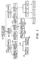
- Figure 1 depicts instruction sets in accordance with the invention.
- Figure 2 shows an embodiment of the invention in the form of an instruction sequence for long displacement load and store.
- Figures 3A-3C show specific load examples of the instruction sequence of Figure 2; Figure 3A shows LOAD WORD, Figure 3B shows LOAD WORD MODIFY, and Figure 3C shows LOAD BYTE.
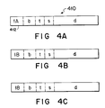
- Figures 4A-4C show specific store examples of the instruction sequence of Figure 2; Figure 4A shows STORE WORD, Figure 4B shows STORE WORD MODIFY, and Figure 4C shows STORE BYTE.
- Figure 5 shows an embodiment of the invention in the form of an instruction sequence for indexed load.
- Figures 6A-6B show specific examples of the instruction sequence of Figure 5; Figure 6A shows LOAD WORD INDEXED and Figure 6B shows LOAD BYTE INDEXED.
- Figure 7 shows an alternate embodiment of the invention in the form of an instruction sequence for short displacement load and store.
- Figures 8A-8B show specific examples of the instruction sequence of Figure 7; Figure 8A shows LOAD WORD SHORT and Figure 8B shows LOAD BYTE SHORT.
- Figures 9A-9C show specific examples of the instruction sequence of Figure 7; Figure 9A shows STORE WORD SHORT, Figure 9B shows STORE BYTE SHORT, and Figure 9C shows STORE BYTES SHORT.
- Figure 10 illustrates an apparatus for address modification in accordance with the invention.
- Figure 11 shows the format of the major operation code representing the instructions of Figures 5 and 7.
- Basically, the means and method in accordance with the invention provide a set of
instructions 110 as shown in Figure 1 for loading and storing data efficiently and expeditiously. Each instruction is designed such that it may be executed within a single cycle of the computer system. Examples of such instruction sets are illustrated in Figures 2, 5, and 7. Examples illustrating such instructions are shown in the remaining figures. - In the case of an instruction set for
long displacement 210 as shown in Figure 2, a field "d" 212 is specified in the instruction sequence. This "d"field 212 defines the amount of displacement, or increment, a pointer, for example, in a register stack, moves. An address can also be modified with this instruction; thisaddress modification 112 can be modified, for example, by a further field embedded in theinstruction sequence 114; this field determines whether such a modification is to take place before data is stored or loaded 116, or after data is stored or loaded 118. This field is the sign bit for thedisplacement word 212. Examples of this long displacement instruction set are shown in Figures 3A-C for loading and in Figures 4A-C for storing. And because the sign bit is already part of the long displacement, no extra or special bit is required for providing this pre- or post-modification information so that whatever bit is available in the instruction string can be used for specifying the displacement. The net result is a displacement specifier that can represent most of the displacement values that are required. - In the case of an instruction set for an indexed load or
store 510, the instructions enable loading of data with apossible address modification 120. Whenaddress modification 120 is specified with an "m"field 520, then the index register can be shifted 122 or left unshifted 124. This index shift or not 122, 124 is determined by a "u"field 522. Examples of thisinstruction set 510 are shown in Figures 6A-6B. - Figure 7 shows the case of an
instruction 710 for short displacement load or store. Theinstruction sequence 710 is defined such that a field "m" 720 determines whether or not an address modification is to be made. When one is made, a further embeddedfield 724 determines whether the modification is made pre- or post-load or store. In this way, a flexible method of handling data in an autonomous manner is achieved. Examples of instructions of this sort are shown in Figures 8A-B for short displacement loading and Figures 9A-C for short displacement storing. - To effect some of these instructions in accordance with the invention, certain preliminary operations need be made and used, namely,
memory load
mem load(addr,low,high), and
memory store
mem store(addr,low,high,data)
are used. These operations are described in the ensuing paragraphs. - 1. For a memory load operation "mem load(addr,low,high)":
- a. when virtual memory translation is on, that is, when the processor status word (PSW) D-bit is "1", then the memory to be loaded from "mem load" is the virtual memory with an address comprising the range of bits of virtual memory from the low bit "low" to the high bit "high" beyond the beginning of the byte of virtual memory with address "addr", where "addr" is a 64-bit virtual address;
- b. otherwise, the memory to be loaded from "mem load" is the real memory with an address comprising the range of bits of real memory from the low bit "low" to the high bit "high" beyond the beginning of the byte of real memory with an address comprising the 32 low order bits, that is, bits 32nd to 63rd, of memory "addr".
- 2. For a memory store operation "mem store(addr,low,high,data)":
- a. when virtual memory translation is on, that is, when the processor status word (PSW) D-bit is "1", then "data" is assigned to the virtual memory with an address comprising the range of bits of virtual memory from the low bit "low" to the high bit "high" beyond the beginning of the byte of real memory with address "addr", where "addr" is a 64-bit virtual address; and
- b. otherwise, "data" is assigned to the real memory with an address comprising the range of bits of real memory from the low bit "low" to the high bit "high" beyond the beginning of the byte of real memory with an address comprising the 32 low order bits, that is, bits 32nd to 63rd, of memory "addr".
- The effective address generated for an
instruction 210 in Figures 1 and 2 is "eff addr1(b,d,s,w,m)", which is calculated as follows: - a. if d < 0 or m = 0, then return the value of "y" with its "w" low-order bits set to zero and assign this to "offset", where "y" is the value of general register "b" added to the value of "d" whose bits are extended to the left with sign bits to a 32-bit quantity taking the rightmost bit as the sign bit;
- b. otherwise, return the value of "y" with its "w" low-order bits set to zero and assign this to "offset", where "y" is the value of general register "b" only;
- c. If s = 0, then assign to "space" the value of the space register having an address comprising 4 added to the high two
bits - d. otherwise, assign the value of space register "s" to "space";
- e. then concatenate "space" and "offset" and assign the result to "eff addr1".
- In other words, in the preferred embodiment, the effective space number is the contents of space register "s" if "s" is nonzero, or is the contents of the space register whose number is the sum of 4 and the two high-order bits of general register "b" if "s" is zero. Also, the 14-bit byte displacement d is in 2's complement notation with the sign bit as its rightmost bit.
- For instructions other than those for "load a word and modify" and "store a word and modify", an effective offset "offset" is determined by the sum of the contents of general register "b" and the sign-extended displacement "d", with the appropriate number of low-order bits ignored. And for instructions for "load a word and modify" and "store a word and modify", the effective offset "offset" depends on the sign of the displacement "d". If "d" is negative as indicated by its sign bit, the effective offset is the sign-extended value of "d" added to the general register "b", with the appropriate number of low-order bits ignored. This effective offset is the value stored into general register "b" (pre-decrement). If "d" is nonnegative, the effective offset is the original contents of general register "b", with the appropriate number of low-order bits ignored. The sum of the contents of general register "b" and the sign-extended value of "d" is stored into the general register "b" (post-increment).
- As examples of the implementation of the invention,
operation codes 214, or opcodes, are used fob long displacement load andstore instructions 210. Theseopcodes 214 specify the particular data transfer to be performed; they also specify whether address modification is to take place. These opcodes has the general format shown in Figure 2, namely,
op / b / t / s / d,
where:
op is a 6-bit field 214 specifying the operation code, e.g., load or store, address modification or not, and data size (word, halfword, or byte);
b is a five-bit field 216 identifying the source register;
t is a five-bit field 218 identifying the target register;
s is a two-bit field 220 specifying a space register; and
d is a 14-bit field 212 specifying a displacement. - As a first example, the instruction for loading a word in a general register is
LDW d(s,b),t
and has the specific format shown in Figure 3A, namely,
12 / b / t / s / d,
where 12 is the 6-bit opcode 314 for the instruction LOAD WORD (LDW). - The
instruction LDW 310 initially calculates an effective address "eff addr1" and then loads the aligned word at that address into the general register "t". Specifically, its operation is as follows: - 1 . During the first cycle, T:
"eff addr1(b,d,s,2,0)" is assigned to "addr"; and - 2. during the second cycle, T + 1:
"mem load(addr,0,31)" is assigned to general register "t", where "eff addr1" and "mem load" are as described earlier. - As a second example, the instruction for loading a word into a general register and then performing an address modification is
LDWM d(s,b),t
and has the specific format shown in Figure 3B, namely,
13 / b / t / s / d,
where 13 is the 6-bit opcode 316 for the instruction LOAD WORD and MODIFY (LDWM). - This
instruction 311 calculates an effective address "eff addr1" and loads the aligned word at that address into the general register "t". The contents of general register "b" is either pre-decremented or post-incremented by the absolute value of the displacement "d" 318, according to the sign of thedisplacement 318. Specifically, the operation of theinstruction 311 is as follows: - 1. During the first cycle, T:
- a. "eff addr1(b,d,s,2,1)" is assigned to "addr"; and
- b. the sum of the contents of general register "b" and the quantity resulting from removing the low-order bit of "d" 318 and extending the remainder on the left with sign bits to a 32-bit quantity, taking the removed bit as the sign bit, is assigned to general register "b".
- 2. During the second cycle, T + 1:
"mem load(addr,0,31)" is assigned to general register "t".
As a third example, the instruction for storing a word from a general register is
STW t,d(s,b)
and has the specific format shown in Figure 4A, namely,
1A / b / t / s / d,
where 1A is the 6-bit opcode 412 for the instruction STORE WORD (STW) 410. Specifically, theinstruction 410 initially calculates an effective address "eff addr1" and stores the contents of general register "t" into the aligned word at that address. In operation, theinstruction 410 proceeds as follows:
During the first cycle, T:- a. the contents of effective address "eff addr1(b,d,s,2,0)" is assigned to "addr"; and
- b. a memory store as described earlier is made for "mem store(addr,0,31,GR[t])", where GR[t] is general register "t".
- An alternate embodiment of the invention is the instruction for indexed
loads 510 in Figure 5 and the instruction for short displacement loads andstores 710 in Figure 7. The general format of an indexed load instruction is shown in Figure 5, namely,
03 / b / x / s / u / 0 / cc / e / m / t
and of short displacement loads and stores is shown in Figure 7, that is,
03 / b / f / s / a / l / cc / e / m / f',
where:
03 is a 6-bit field code
b is a 5-bit field
x is a 5-bit field 516 identifying a source register "x";
f is a 5-bit field 716 identifying a signed immediate field in the case of load instructions and a control source register in the case of store instructions;
s is a 2-bit field
u is a 1-bit specifier 522, where a "0" indicates an index register, and a "1" indicates an index register shifted by the data size, that is, the index value is multiplied by the size of the data item being loaded;
a is a premodify orpostmodify bit 724, where, whenever themodification bit 520, 720 m = 1, "0" signifies modification after data movement and "1" signifies modification before data movement;
cc is a 2-bit field
e is a 4-bit field
m is a modifybit 520, 720;
t is a 5-bit field 530 identifying a source register "t" in the case of store instructions and a target register "t" in the case of load instructions; and
f' is a 5-bit field 730 identifying a target register in the case of load instructions and an immediate field in the case of store instructions. - Note that the formats in Figures 5 and 7 are identical but for the "x"/"f", "a"/"u" and "0"/"1" pairs. They have a common opcode of "03". The "x" and "f" fields can both be represented by "F", a 5-bit field that identifies an immediate or a register. Likewise, the other pairs can be represented by a "U" field and an "L" field; these fields are described below. The remaining fields in combination with these fields distinguish the different operations within this major operation code. The result, as shown in Figure 11, is a
major operation code 1110 representing the instructions in both Figures 5 and 7. In Figure 11, the "e" field is described in further details. - The format of the major instruction shown in Figure 11 is reproduced here:
03 / b / F / s / U / L / cc / D / E / S / m / T,
where:
F is a 5-bit displacement field 1114 representing either "x" 516 or "f" 716 as before;
U is a 5-bit field 1116 representing either "u" 522 or "a" 724 as before;
L is a 1-bit literal 1118, where a "1" signifies using an immediate as a displacement and a "0" signifies using the value of an index register as a displacement;
D is a 1-bit field 1120, where a "1" signifies store and a "0" signifies load;
E is a 1-bit field 1122 to signify special operation, e.g., store byte or store bytes;
S is a 2-bit field 1124 for specifying data size, that is, "00" means no shift, or byte; "01" meansshift 1, or halfword; "10" meansshift 2, or word; and "11" means shift 3, or double word;
T is a 5-bit field 1126 representing "t" 530 or "f'" 730 as before; and
"b", "s", "cc", and "m" are as before. - In this format, the concatenation 1112 of fields "D", "E" and "S" represent the previously described 4-bit field "e" 528, 728 used for code extension.
- The cache control bits "cc" 526, 726 in the instructions in accordance with the invention provide a special advantage to the computer system using a cache memory. This "cc" field, which is imbedded within the instruction, provides cache hints to the cache memory. These cache hints are information encoded to identify the data structure being accessed by the load or store data instruction, e.g., STACK POP for load, STACK PUSH for store, SEQUENTIAL READ for load, and SEQUENTIAL WRITE for store. This optional information that is supplied may be used by a cache controller to reduce cache misses, to reduce memory traffic between cache and main memory, to determine whether or not to prefetch the next cache line, and to provide any other instructions that would improve the performance of the cache memory.
- If address modification is specified in an indexed load, an effective offset "offset" is defined as the contents of the general register "b" in a postmodify situation. Address modification results in replacing the contents of general register "b" by the sum of the index value, possibly shifted by the data size, and the previous contents of general register "b". This operation is given by the following two routines:
- 1. For the index value "ind val(x,sh,u)", the following operation is made:
- a. if u = 0, then the value of general register "x" is assigned to "ind val";
- b. otherwise, the value of general register "x", left-shifted by "sh", is assigned to "ind val".
- 2. For calculating the "eff addr2(b,s,x,m,u,sh)", an effective address, the following operation is made:
- a. if m = 1, then the value of general register "b" with its "sh" low-order bits set to zero is assigned to effective offset "offset";
- b. otherwise, the sum of the value of general register "b" and "ind val(x,sh,u)", as defined above, with its "sh" low-order bits set to zero, is assigned to effective offset "offset"; and
- c. if s = 0, then the value of the space register having an address comprising the value of the first two high-order bits "0" and "1" of general register "b" added to 4 is assigned to a space register "space";
- d. otherwise, the contents of space register "s" is assigned to a space register "space"; and
- e. the concatenation of the values of "space" and "offset" is assigned to effective address "eff addr2".
- As a first example, the instruction for loading an
index word 610 is
LDWX,u,m,cc x(s,b),t
and has the format as shown in Figure 6A, namely,
03 / b / x / s / u / 0 / cc / 2 / m / t,
where 03 is theopcode 612 for the operation LOAD WORD INDEXED (LDWX). Its operation is as follows: - 1. During the first cycle, T:
- a. effective address "eff addr2(b,s,x,m,u,2)" is assigned an address "addr"; and
- b. the value of general register "b" added to the index value "ind val(x,2,u)" replaces the original value in general register "b".
- 2. During the second cycle, T + 1:
the contents of the load memory "mem load(addr,0,31)",
described above, is assigned to general register "t". - As a second example, the instruction for storing a short word (STORE WORD SHORT) 910 is
STWS,m,a,cc t,i(s,b)
and has the format as shown in Figure 9A, namely,
03 / b / t / s / a / l / cc / A / m / i,
where the fields are as described in the general format and:
03 is a 6-bit field 912 specifying the operation code for STORE WORD SHORT; and
A is a 4-bit field 914 specifying an operation code extension. - This
instruction 910 calculates an effective address "eff addr3" and the value of general register "t" is stored into the aligned word at that address. Specifically, - 1. During the cycle T:
- a. effective address "eff addr3(b,i,s,a,m,2)" is calculated analogously to the previous calculation for "eff addr2(b,s,x,m,u,sh)", above, and the value thereto is assigned to an address "addr";
- b. if the modification bit 916 m = 1, that is, if modify is specified, then the value of general register "b" is added to "low sign ext(i)", which is calculated analogously to that in previous examples, and the sum value is assigned to general register "b"; in other words, the original value of general register "b" is replaced with the sum; and
- 2. during the second cycle, T + 1, the operation "mem store(addr,0,31,GR[t])" described above is made.
- In all the above examples, in a pipelined computer system, the first cycle T of a subsequent load or store instruction (LOAD, STORE) may be executed simultaneously with the second cycle (T + 1) of a current load or store instruction so that the effective execution time for one load or store instruction is still one cycle.
- Figure 10 shows an apparatus in accordance with the preferred embodiment for implementing a load or store instruction having a code for address modification. Accordingly, values of a base register "b" (not shown) and an index register "x" (not shown) are read onto a "b"
register bus 1012 and anindex register bus 1014, respectively, from ageneral register file 1010. Theindex register bus 1014 is coupled to a four-to-one multiplexer 1016; it is also coupled to themultiplexer 1016 as a shiftedvalue 1018. Also coupled to themultiplexer 1016 arevalues instruction register 1020. Thesevalues bus 1012 and theoutput 1026 of themultiplexer 1016 are coupled to an arithmetic logic unit (ALU) 1028, where address generation is performed in response to the twoinputs result 1030 from theALU 1028 is used for address modification by coupling it through anoptional pipeline register 1032 on aresult bus 1034 back to thegeneral register file 1010, where the modified address generated is assigned in the base register (not shown). The registers in thegeneral register 1010 are addressed through anaddress decoder 1036, which responds to inputs from theinstruction register 1020. Theoutput 1030 of theALU 1028 is also coupled to acache memory 1038 through a two-to-one multiplexer 1040 and anoptional pipeline register 1042. The two-to-one multiplexer 1040 has as its inputs the "b"register value 1012 and the modifiedaddress 1030.Data 1046 addressed by theoutput 1048 of the two-to-one multiplexer 1040 in thecache memory 1038 anddata 1050 from thegeneral register file 1010 are loaded to thegeneral register file 1010 and thecache memory 1038, respectively. The two-to-one multiplexer 1040 is responsive to a pre- or post-modification specifier, and the four-to-one multiplexer 1016 is responsive to a displacement specifier. The hardware elements shown in Figure 10 are those found in all computer systems; no special or additional hardware elements are required to implement the instruction for load and store data with address modification to result in a highly efficient and greatly simplified one-cycle operation of the instruction.
Claims (9)
- A computer system comprising:A. an instruction comprising:a. a first field (b) specifying a base register;b. a second field (d) specifying a displacement; andc. a third field (m) specifying modification of a selected address; andB. means for performing operations in response to said instruction;
characterised in that:
said first, second and third fields are comprised in a single instruction suitable for operation within a single cycle of said computer system, and
wherein said displacement is either the value of an index (u) shifted or unshifted or a displacement shifted by a data size as determined by fields embedded within said single instruction. - A system according to claim 1 wherein said instruction further comprises a fourth field (116,118), also forming part of said single instruction, specifying modification of a selected address before or after a selected operation.
- A system according to claim 2 wherein said fourth field is the sign bit of said second field.
- A system according to claim 3 wherein said fourth field is a single bit.
- A system according to any of claims 1 to 4 wherein said second field (d) is a field for specifying immediate data.
- A method for transferring data between a first and second storage device in a computer system comprising:
providing an instruction comprising:a. a first field (b) specifying a base register;b. a second field (d) specifying a displacement; andc. a third field (m) specifying modification of a selected address, andperforming operations in response to said instruction;
characterised in that:
said first, second and third fields are comprised in a single instruction suitable for operation within a single cycle of said computer system, and
wherein said displacement is either the value of an index (u) shifted or unshifted or a displacement shifted by a data size as determined by fields embedded within said single instruction. - A method according to claim 6, comprising the steps of:
locating a base address and a displacement from an instruction within a cycle of said computer system;
identifying from said instruction within said cycle of said computer system a selected method from a plurality of methods for forming an address to said first storage device;
determining from a sign bit of said displacement when said base address will be augmented by said displacement;
forming said address according to said instruction within said cycle of said computer system; and
transferring data between said second storage device and said address of said first storage device within said cycle of said computer system. - A method according to claim 6, comprising the steps of:
locating a base address and an index register from an instruction within a cycle of said computer system;
identifying from said instruction within said cycle of said computer how much the contents of said index register will be shifted;
shifting said contents of said index register in response to said instruction within said cycle of said computer system;
determining from said instruction within said cycle of said computer system when to augment the contents of said base register with said contents of said shifted index register;
forming an address to said first storage device in response to said instruction within said cycle of said computer by summing said contents of said index register and said base address;
augmenting said contents of said base register within said cycle of said computer system according to said instruction; and
transferring data between said second storage device and said address of said first storage device within said cycle of said computer system. - A method according to claim 6, comprising the steps of:
identifying a base address, a displacement, and data size from an instruction within a cycle of said computer system;
shifting said displacement by said data size in response to said instruction within said cycle of said computer system;
identifying from said instruction within said cycle of said computer system when said base register is augmented by said shifted displacement;
forming an address to said first storage device by adding said shifted displacement to the contents of said base register within said cycle of said computer system;
augmenting said contents of said base register according to said instruction within said cycle of said computer and
transferring data between said second storage device and said address of said first storage device within said cycle of said computer system.
Applications Claiming Priority (2)
| Application Number | Priority Date | Filing Date | Title |
|---|---|---|---|
| US75081085A | 1985-06-28 | 1985-06-28 | |
| US750810 | 1985-06-28 |
Publications (3)
| Publication Number | Publication Date |
|---|---|
| EP0206653A2 EP0206653A2 (en) | 1986-12-30 |
| EP0206653A3 EP0206653A3 (en) | 1988-10-26 |
| EP0206653B1 true EP0206653B1 (en) | 1992-10-21 |
Family
ID=25019262
Family Applications (1)
| Application Number | Title | Priority Date | Filing Date |
|---|---|---|---|
| EP19860304493 Expired EP0206653B1 (en) | 1985-06-28 | 1986-06-12 | Method and means for loading and storing data in a reduced instruction set computer |
Country Status (4)
| Country | Link |
|---|---|
| EP (1) | EP0206653B1 (en) |
| JP (1) | JPS623334A (en) |
| CA (1) | CA1273435A (en) |
| DE (1) | DE3686984T2 (en) |
Cited By (4)
| Publication number | Priority date | Publication date | Assignee | Title |
|---|---|---|---|---|
| US7197601B2 (en) | 2003-05-12 | 2007-03-27 | International Business Machines Corporation | Method, system and program product for invalidating a range of selected storage translation table entries |
| US9182984B2 (en) | 2012-06-15 | 2015-11-10 | International Business Machines Corporation | Local clearing control |
| US9241735B2 (en) | 2003-12-05 | 2016-01-26 | Onset Medical Corporation | Expandable percutaneous sheath |
| US9454490B2 (en) | 2003-05-12 | 2016-09-27 | International Business Machines Corporation | Invalidating a range of two or more translation table entries and instruction therefore |
Families Citing this family (6)
| Publication number | Priority date | Publication date | Assignee | Title |
|---|---|---|---|---|
| DE69315630T2 (en) * | 1992-07-23 | 1998-07-16 | Rockwell International Corp | Data access in a RISC digital signal processor |
| WO1997031310A1 (en) * | 1996-02-23 | 1997-08-28 | Advanced Micro Devices, Inc. | A microprocessor configured to execute instructions which specify increment of a source operand |
| US6990570B2 (en) | 1998-10-06 | 2006-01-24 | Texas Instruments Incorporated | Processor with a computer repeat instruction |
| DE69839910D1 (en) * | 1998-10-06 | 2008-10-02 | Texas Instruments Inc | Method and apparatus for iterative command execution |
| US7103754B2 (en) | 2003-03-28 | 2006-09-05 | International Business Machines Corporation | Computer instructions for having extended signed displacement fields for finding instruction operands |
| US7356710B2 (en) * | 2003-05-12 | 2008-04-08 | International Business Machines Corporation | Security message authentication control instruction |
-
1986
- 1986-06-12 EP EP19860304493 patent/EP0206653B1/en not_active Expired
- 1986-06-12 DE DE19863686984 patent/DE3686984T2/en not_active Expired - Fee Related
- 1986-06-20 JP JP61144654A patent/JPS623334A/en active Pending
- 1986-06-27 CA CA000512684A patent/CA1273435A/en not_active Expired
Cited By (9)
| Publication number | Priority date | Publication date | Assignee | Title |
|---|---|---|---|---|
| US7197601B2 (en) | 2003-05-12 | 2007-03-27 | International Business Machines Corporation | Method, system and program product for invalidating a range of selected storage translation table entries |
| US7281115B2 (en) | 2003-05-12 | 2007-10-09 | International Business Machines Corporation | Method, system and program product for clearing selected storage translation buffer entries |
| US7284100B2 (en) | 2003-05-12 | 2007-10-16 | International Business Machines Corporation | Invalidating storage, clearing buffer entries, and an instruction therefor |
| US7890731B2 (en) | 2003-05-12 | 2011-02-15 | International Business Machines Corporation | Clearing selected storage translation buffer entries based on table origin address |
| US8122224B2 (en) | 2003-05-12 | 2012-02-21 | International Business Machines Corporation | Clearing selected storage translation buffer entries bases on table origin address |
| US8452942B2 (en) | 2003-05-12 | 2013-05-28 | International Business Machines Corporation | Invalidating a range of two or more translation table entries and instruction therefore |
| US9454490B2 (en) | 2003-05-12 | 2016-09-27 | International Business Machines Corporation | Invalidating a range of two or more translation table entries and instruction therefore |
| US9241735B2 (en) | 2003-12-05 | 2016-01-26 | Onset Medical Corporation | Expandable percutaneous sheath |
| US9182984B2 (en) | 2012-06-15 | 2015-11-10 | International Business Machines Corporation | Local clearing control |
Also Published As
| Publication number | Publication date |
|---|---|
| DE3686984D1 (en) | 1992-11-26 |
| EP0206653A3 (en) | 1988-10-26 |
| EP0206653A2 (en) | 1986-12-30 |
| CA1273435A (en) | 1990-08-28 |
| DE3686984T2 (en) | 1993-03-11 |
| JPS623334A (en) | 1987-01-09 |
Similar Documents
| Publication | Publication Date | Title |
|---|---|---|
| US4454578A (en) | Data processing unit with pipelined operands | |
| US5809306A (en) | Variable address length compiler and processor improved in address management | |
| KR100327776B1 (en) | Data processing method using multiple instruction sets | |
| US5717946A (en) | Data processor | |
| US5522051A (en) | Method and apparatus for stack manipulation in a pipelined processor | |
| EP0415461B1 (en) | Central processing unit supporting variable length instructions | |
| US6253311B1 (en) | Instruction set for bi-directional conversion and transfer of integer and floating point data | |
| US20060174089A1 (en) | Method and apparatus for embedding wide instruction words in a fixed-length instruction set architecture | |
| US5249280A (en) | Microcomputer having a memory bank switching apparatus for accessing a selected memory bank in an external memory | |
| JPH0926878A (en) | Data processing device | |
| KR20180067582A (en) | Vector load instruction | |
| US7574583B2 (en) | Processing apparatus including dedicated issue slot for loading immediate value, and processing method therefor | |
| KR20180066146A (en) | Vector data transfer instruction | |
| USRE32493E (en) | Data processing unit with pipelined operands | |
| US5590358A (en) | Processor with word-aligned branch target in a byte-oriented instruction set | |
| KR100682635B1 (en) | Microprocessor containing multiple register files occupying the same logical space | |
| US5717910A (en) | Operand compare/release apparatus and method for microinstrution sequences in a pipeline processor | |
| JPH07120278B2 (en) | Data processing device | |
| EP0206653A2 (en) | Method and means for loading and storing data in a reduced instruction set computer | |
| JP2001523022A (en) | Computer processor and method for data streaming | |
| US4812971A (en) | Central processing unit for a digital computer | |
| US4893235A (en) | Central processing unit for a digital computer | |
| US4608633A (en) | Method for decreasing execution time of numeric instructions | |
| CA1254661A (en) | Method and means for instruction combination for code compression | |
| US20020108029A1 (en) | Program counter (PC) relative addressing mode with fast displacement |
Legal Events
| Date | Code | Title | Description |
|---|---|---|---|
| PUAI | Public reference made under article 153(3) epc to a published international application that has entered the european phase |
Free format text: ORIGINAL CODE: 0009012 |
|
| AK | Designated contracting states |
Kind code of ref document: A2 Designated state(s): CH DE FR GB IT LI NL SE |
|
| PUAL | Search report despatched |
Free format text: ORIGINAL CODE: 0009013 |
|
| RHK1 | Main classification (correction) |
Ipc: G06F 9/30 |
|
| AK | Designated contracting states |
Kind code of ref document: A3 Designated state(s): CH DE FR GB IT LI NL SE |
|
| 17P | Request for examination filed |
Effective date: 19890407 |
|
| 17Q | First examination report despatched |
Effective date: 19901122 |
|
| GRAA | (expected) grant |
Free format text: ORIGINAL CODE: 0009210 |
|
| AK | Designated contracting states |
Kind code of ref document: B1 Designated state(s): CH DE FR GB IT LI NL SE |
|
| REF | Corresponds to: |
Ref document number: 3686984 Country of ref document: DE Date of ref document: 19921126 |
|
| ET | Fr: translation filed | ||
| ITF | It: translation for a ep patent filed | ||
| ITTA | It: last paid annual fee | ||
| PLBE | No opposition filed within time limit |
Free format text: ORIGINAL CODE: 0009261 |
|
| STAA | Information on the status of an ep patent application or granted ep patent |
Free format text: STATUS: NO OPPOSITION FILED WITHIN TIME LIMIT |
|
| 26N | No opposition filed | ||
| EAL | Se: european patent in force in sweden |
Ref document number: 86304493.9 |
|
| PGFP | Annual fee paid to national office [announced via postgrant information from national office to epo] |
Ref country code: DE Payment date: 19990521 Year of fee payment: 14 |
|
| NLS | Nl: assignments of ep-patents |
Owner name: HEWLETT-PACKARD COMPANY (A DELAWARE CORPORATION) |
|
| REG | Reference to a national code |
Ref country code: GB Ref legal event code: 732E |
|
| REG | Reference to a national code |
Ref country code: FR Ref legal event code: TP |
|
| REG | Reference to a national code |
Ref country code: CH Ref legal event code: PFA Free format text: HEWLETT-PACKARD COMPANY TRANSFER- HEWLETT-PACKARD COMPANY, A DELAWARE CORPORATION |
|
| PG25 | Lapsed in a contracting state [announced via postgrant information from national office to epo] |
Ref country code: DE Free format text: LAPSE BECAUSE OF NON-PAYMENT OF DUE FEES Effective date: 20010403 |
|
| REG | Reference to a national code |
Ref country code: GB Ref legal event code: IF02 |
|
| PGFP | Annual fee paid to national office [announced via postgrant information from national office to epo] |
Ref country code: NL Payment date: 20050516 Year of fee payment: 20 |
|
| PGFP | Annual fee paid to national office [announced via postgrant information from national office to epo] |
Ref country code: GB Payment date: 20050608 Year of fee payment: 20 |
|
| PGFP | Annual fee paid to national office [announced via postgrant information from national office to epo] |
Ref country code: FR Payment date: 20050617 Year of fee payment: 20 |
|
| PGFP | Annual fee paid to national office [announced via postgrant information from national office to epo] |
Ref country code: SE Payment date: 20050621 Year of fee payment: 20 |
|
| PGFP | Annual fee paid to national office [announced via postgrant information from national office to epo] |
Ref country code: CH Payment date: 20050622 Year of fee payment: 20 |
|
| PGFP | Annual fee paid to national office [announced via postgrant information from national office to epo] |
Ref country code: IT Payment date: 20050629 Year of fee payment: 20 |
|
| PG25 | Lapsed in a contracting state [announced via postgrant information from national office to epo] |
Ref country code: GB Free format text: LAPSE BECAUSE OF EXPIRATION OF PROTECTION Effective date: 20060611 |
|
| PG25 | Lapsed in a contracting state [announced via postgrant information from national office to epo] |
Ref country code: NL Free format text: LAPSE BECAUSE OF EXPIRATION OF PROTECTION Effective date: 20060612 |
|
| REG | Reference to a national code |
Ref country code: GB Ref legal event code: PE20 |
|
| REG | Reference to a national code |
Ref country code: CH Ref legal event code: PL |
|
| NLV7 | Nl: ceased due to reaching the maximum lifetime of a patent |
Effective date: 20060612 |
|
| EUG | Se: european patent has lapsed |