EP0206619B1 - Self-soldering, flexible circuit connector - Google Patents
Self-soldering, flexible circuit connector Download PDFInfo
- Publication number
- EP0206619B1 EP0206619B1 EP86304393A EP86304393A EP0206619B1 EP 0206619 B1 EP0206619 B1 EP 0206619B1 EP 86304393 A EP86304393 A EP 86304393A EP 86304393 A EP86304393 A EP 86304393A EP 0206619 B1 EP0206619 B1 EP 0206619B1
- Authority
- EP
- European Patent Office
- Prior art keywords
- flexible circuit
- conductors
- heater
- exposed
- assembly according
- Prior art date
- Legal status (The legal status is an assumption and is not a legal conclusion. Google has not performed a legal analysis and makes no representation as to the accuracy of the status listed.)
- Expired - Lifetime
Links
Images


Classifications
-
- H—ELECTRICITY
- H05—ELECTRIC TECHNIQUES NOT OTHERWISE PROVIDED FOR
- H05K—PRINTED CIRCUITS; CASINGS OR CONSTRUCTIONAL DETAILS OF ELECTRIC APPARATUS; MANUFACTURE OF ASSEMBLAGES OF ELECTRICAL COMPONENTS
- H05K3/00—Apparatus or processes for manufacturing printed circuits
- H05K3/36—Assembling printed circuits with other printed circuits
- H05K3/361—Assembling flexible printed circuits with other printed circuits
- H05K3/363—Assembling flexible printed circuits with other printed circuits by soldering
-
- H—ELECTRICITY
- H05—ELECTRIC TECHNIQUES NOT OTHERWISE PROVIDED FOR
- H05K—PRINTED CIRCUITS; CASINGS OR CONSTRUCTIONAL DETAILS OF ELECTRIC APPARATUS; MANUFACTURE OF ASSEMBLAGES OF ELECTRICAL COMPONENTS
- H05K1/00—Printed circuits
- H05K1/02—Details
- H05K1/0201—Thermal arrangements, e.g. for cooling, heating or preventing overheating
- H05K1/0212—Printed circuits or mounted components having integral heating means
-
- H—ELECTRICITY
- H05—ELECTRIC TECHNIQUES NOT OTHERWISE PROVIDED FOR
- H05K—PRINTED CIRCUITS; CASINGS OR CONSTRUCTIONAL DETAILS OF ELECTRIC APPARATUS; MANUFACTURE OF ASSEMBLAGES OF ELECTRICAL COMPONENTS
- H05K1/00—Printed circuits
- H05K1/02—Details
- H05K1/0213—Electrical arrangements not otherwise provided for
- H05K1/0237—High frequency adaptations
- H05K1/0242—Structural details of individual signal conductors, e.g. related to the skin effect
-
- H—ELECTRICITY
- H05—ELECTRIC TECHNIQUES NOT OTHERWISE PROVIDED FOR
- H05K—PRINTED CIRCUITS; CASINGS OR CONSTRUCTIONAL DETAILS OF ELECTRIC APPARATUS; MANUFACTURE OF ASSEMBLAGES OF ELECTRICAL COMPONENTS
- H05K2201/00—Indexing scheme relating to printed circuits covered by H05K1/00
- H05K2201/04—Assemblies of printed circuits
- H05K2201/049—PCB for one component, e.g. for mounting onto mother PCB
-
- H—ELECTRICITY
- H05—ELECTRIC TECHNIQUES NOT OTHERWISE PROVIDED FOR
- H05K—PRINTED CIRCUITS; CASINGS OR CONSTRUCTIONAL DETAILS OF ELECTRIC APPARATUS; MANUFACTURE OF ASSEMBLAGES OF ELECTRICAL COMPONENTS
- H05K2201/00—Indexing scheme relating to printed circuits covered by H05K1/00
- H05K2201/05—Flexible printed circuits [FPCs]
- H05K2201/056—Folded around rigid support or component
-
- H—ELECTRICITY
- H05—ELECTRIC TECHNIQUES NOT OTHERWISE PROVIDED FOR
- H05K—PRINTED CIRCUITS; CASINGS OR CONSTRUCTIONAL DETAILS OF ELECTRIC APPARATUS; MANUFACTURE OF ASSEMBLAGES OF ELECTRICAL COMPONENTS
- H05K2201/00—Indexing scheme relating to printed circuits covered by H05K1/00
- H05K2201/08—Magnetic details
- H05K2201/083—Magnetic materials
-
- H—ELECTRICITY
- H05—ELECTRIC TECHNIQUES NOT OTHERWISE PROVIDED FOR
- H05K—PRINTED CIRCUITS; CASINGS OR CONSTRUCTIONAL DETAILS OF ELECTRIC APPARATUS; MANUFACTURE OF ASSEMBLAGES OF ELECTRICAL COMPONENTS
- H05K2201/00—Indexing scheme relating to printed circuits covered by H05K1/00
- H05K2201/10—Details of components or other objects attached to or integrated in a printed circuit board
- H05K2201/10613—Details of electrical connections of non-printed components, e.g. special leads
- H05K2201/10621—Components characterised by their electrical contacts
- H05K2201/10727—Leadless chip carrier [LCC], e.g. chip-modules for cards
-
- H—ELECTRICITY
- H05—ELECTRIC TECHNIQUES NOT OTHERWISE PROVIDED FOR
- H05K—PRINTED CIRCUITS; CASINGS OR CONSTRUCTIONAL DETAILS OF ELECTRIC APPARATUS; MANUFACTURE OF ASSEMBLAGES OF ELECTRICAL COMPONENTS
- H05K2203/00—Indexing scheme relating to apparatus or processes for manufacturing printed circuits covered by H05K3/00
- H05K2203/11—Treatments characterised by their effect, e.g. heating, cooling, roughening
- H05K2203/1115—Resistance heating, e.g. by current through the PCB conductors or through a metallic mask
-
- H—ELECTRICITY
- H05—ELECTRIC TECHNIQUES NOT OTHERWISE PROVIDED FOR
- H05K—PRINTED CIRCUITS; CASINGS OR CONSTRUCTIONAL DETAILS OF ELECTRIC APPARATUS; MANUFACTURE OF ASSEMBLAGES OF ELECTRICAL COMPONENTS
- H05K2203/00—Indexing scheme relating to apparatus or processes for manufacturing printed circuits covered by H05K3/00
- H05K2203/15—Position of the PCB during processing
- H05K2203/1581—Treating the backside of the PCB, e.g. for heating during soldering or providing a liquid coating on the backside
-
- H—ELECTRICITY
- H05—ELECTRIC TECHNIQUES NOT OTHERWISE PROVIDED FOR
- H05K—PRINTED CIRCUITS; CASINGS OR CONSTRUCTIONAL DETAILS OF ELECTRIC APPARATUS; MANUFACTURE OF ASSEMBLAGES OF ELECTRICAL COMPONENTS
- H05K3/00—Apparatus or processes for manufacturing printed circuits
- H05K3/22—Secondary treatment of printed circuits
- H05K3/28—Applying non-metallic protective coatings
-
- H—ELECTRICITY
- H05—ELECTRIC TECHNIQUES NOT OTHERWISE PROVIDED FOR
- H05K—PRINTED CIRCUITS; CASINGS OR CONSTRUCTIONAL DETAILS OF ELECTRIC APPARATUS; MANUFACTURE OF ASSEMBLAGES OF ELECTRICAL COMPONENTS
- H05K3/00—Apparatus or processes for manufacturing printed circuits
- H05K3/30—Assembling printed circuits with electric components, e.g. with resistors
- H05K3/32—Assembling printed circuits with electric components, e.g. with resistors electrically connecting electric components or wires to printed circuits
- H05K3/34—Assembling printed circuits with electric components, e.g. with resistors electrically connecting electric components or wires to printed circuits by soldering
- H05K3/3494—Heating processes for reflow soldering
-
- H—ELECTRICITY
- H05—ELECTRIC TECHNIQUES NOT OTHERWISE PROVIDED FOR
- H05K—PRINTED CIRCUITS; CASINGS OR CONSTRUCTIONAL DETAILS OF ELECTRIC APPARATUS; MANUFACTURE OF ASSEMBLAGES OF ELECTRICAL COMPONENTS
- H05K3/00—Apparatus or processes for manufacturing printed circuits
- H05K3/36—Assembling printed circuits with other printed circuits
Definitions
- the present invention relates to flexible circuits and more particularly to flexible circuits and flexible circuit boards having an integral heater.
- IBM Technical Disclosure Bulletin Vol. 9, No. 11, April 1967, page 1668 describes a substrate serving as a mounting board for electronic chip carrier modules which have pins that arc soldered into receptacles or buckets in the substrate.
- an orthogonal matrix of heater wires is embedded in the substrate, with heater terminals arranged around the edges of the substrate, and a power supply is connected to the terminals of selected heater wires that cross over in the region of the solder buckets of any individual module that is to be removed.
- An object of the present invention is to achieve a connection technology, capable of reuse if desired, that combines a high density capability, equivalent to that of an elastomeric connector, with the reliability of a solder joint.
- an electrical circuit assembly for connection to other circuits, comprising one or more electrical conductors embedded in and covered by a body of insulating material having two large opposed surfaces, said conductor or each conductor having a connection region where it is exposed at one of said opposed surfaces, characterised in that the body of insulating material containing the embedded conductor or conductors is flexible and a self-regulating electrical resistance heater to apply heat for making electrical connection, especially soldered connection, and adapted to be energized from a source of substantially constant a.c. current is disposed along the other of said opposed surfaces at the region opposite that where said conductor or conductors are exposed.
- the invention further provides a method of making multiple electrical circuit connections, such as in the connecting together of electrical circuit boards, wherein a first array of exposed portions of otherwise insulated electrical conductors embedded in a circuit board are soldered to a co-operating second array of exposed portions of conductors of another circuit assembly by the application of heat to melt the solder, characterised in that said first array of conductor portions is exposed at one surface of a circuit board made of a flexible insulating material and, after the two arrays of exposed conductor portions have been brought together in assembled alignment and solder has been supplied to their contact surfaces, the heat to melt the solder is generated by a self-regulating electrical resistance heater energised by a substantially constant a.c. current which heater is applied to the other surface of the flexible circuit board opposite to said first array of exposed conductor portions.
- a self-regulating temperature controlled heater of the order of as little as .030 inch (.76mm) thick is applied to the flexible circuit over an area where solder connections between the flexible circuit and another circuit or component are to be made.
- the insulation over the conductors is removed on the side away from the heater and the exposed conductors are covered with solder or other conductive heat-activated material.
- the exposed conductors are tinned and a reflowable solder pad on the board is employed, this combination being preferable in most high density uses.
- the heater is preferably of a type operating in the manner disclosed in U.S. Patent No. 4,256,945.
- Such heaters employ a technique for temperature regulation based on a combination of alternating current skin effect, the Curie point of ferromagnetic material and a relatively constant current supply to cause the heater to maintain a constant temperature determined by the composition of the ferromagnetic material utilised.
- the temperature of the heater typically could be approximately 265°C.
- Flexible circuits with heaters as set forth herein are capable of use to connect pad and pin grid arrays to p.c. boards or the like and to connect, for instance, 166 conductors in a 8.4 inch (213mm) wide circuit having the conductors at .05 inch (1.27mm) centres to a p.c. board or substrate in a surface mount configuration.
- the flexible circuit may be used to interconnect printed circuit boards, leaded and leadless chip carriers to printed circuit boards and printed circuit boards or the equivalent to multiple printed circuit boards. Further, the flexible circuit may be employed in a U-shaped configuration to contact exposed conductors on both sides of a daughter board and to contact conductors on a mother board all at the same time to provide a variety of selectable interconnections.
- FIG. 1 there are illustrated two views of a flexible circuit with an integral heater.
- the flexible circuit generally designated by the reference numeral 2
- the flexible circuit has embedded in an insulating flexible body 4, a plurality of conductors 6.
- the conductors 6 are illustrated for purposes of description only as a series of parallel conductors; it being understood that the conductors can conform to any desired pattern so long as, in the region where connection to an external or internal circuit or connector is to be made, they are arrayed in conformance with the circuit array of that other circuit or connector.
- This region is generally designated by the reference numeral 8.
- the insulation covering the conductors 6 is removed and solder 10 or other heat activated conductive material is applied to the bared conductors 6.
- a heater 12 lies across the region 8 of the flexible circuit, as viewed in Figure 2, being located on the opposite side of the circuit from the bared conductors 6.
- the insulation 4 in this embodiment is brought round to cover the heater and extends beyond the heater, where it is united to the main body of the flexible circuit.
- the heater is sealed into the circuit 2, at the region of the exposed conductors and solder, for heating the solder to its melt temperature and above to such extent as may be desired.
- FIG. 1A an alternative layout of the heater structure is illustrated.
- a heater 5 is again laid across an end region of a flexible circuit board 3 but instead of its end portion extending straight out of the edge of the flexible circuit as in Figure 1, it makes a 90° turn as at 7 and has a length 9 extending along a side edge of the circuit.
- current contact terminals 11 and 13 are provided; and in this embodiment a grommet 15 is passed through the opposite end of the heater remote from the terminals 11 and 13 to electrically connect the various layers together.
- Aligning holes 17 and 19 are provided in the corners of the board 3.
- the heater 12 of Figure 1 is a self-regulating heater.
- a self-regulating heater of the type which may be employed herein includes a conductor 14 surrounded by a thin layer 16 [.002" (.05mm) for instance] of the insulation 4.
- Surrounding the layer 16 is a layer 18 of ferromagnetic material about 1 to 1.8 skin depths thick, itself surrounded by a layer of copper 20.
- the heater illustrated may be 0.030 inch (0.76mm) thick, about 0.180 inch (4.6mm) wide, 9 inches (229mm) long and delivers about 250 watts of power at a temperature of 265°C: about the temperature of a wave solder machine.
- the heater autoregulates at or approaching the Curie temperature of the ferromagnetic layer which in this application is, as indicated above, approximately 265°C.
- Connection to the heater 12 is made at end location 22 of the heater (see Figure 4) where the copper-ferromagnetic outer layers are removed over an area to expose a region of the insulation 16 and a smaller region of the insulation is removed to expose the conductor 14.
- the copper-ferromagnetic layers 20-18 on the one hand and the return conductor 14 on the other hand are connected together electrically at the end of the heater remote from the region 22; that is, at the left end of the heater as viewed in Figure 1. This connection may be achieved simply by discontinuing the insulating layer 16 just short of the end of the heater remote from region 22 and compressing the end portion so that the conductors are all in contact; or the layers may be soldered together.
- the heater 12 is illustrated in Figure 1 as extending outwardly from the flexible circuit 2 but may well be terminated at the edge of the circuit 2 with the region 22 lying outwardly of the outermost conductor 6; or the heater contact area may lie along the side of the flexible circuit as in Figure 1A.
- FIG. 5 and 5A of the accompanying drawings there is illustrated, in pictorial view and side view, the connector region 8 of the flexible circuit 2 of Figure 1 in alignment with a printed circuit board 30 to which the circuit 2 is to be connected.
- the connector 8 is provided with alignment holes 34 to mate with pins 32 on the printed circuit board 30.
- the pins 32 are aligned with holes 34 and the two boards are pressed together while current is applied to the heater 33 through a hole 44 in the upper surface of the circuit as viewed in Figures 5 and 5A.
- a solder carrier pad 35 may also be employed.
- a flexible circuit 50 is provided at its two ends with heater and bared conductor arrangements 52 and 54. These flexible circuit ends may be soldered lead for lead to leads 56 and 58, respectively, on printed circuit boards 60 and 62. In such an arrangement a separate connector is not required since it is standard practice for printed circuit boards to terminate in parallel conductors for insertion into connectors. In such a case, alignment can be obtained by having studs protruding from the printed circuit board for insertion into mating holes in the flexible circuit, by an alignment housing, or, in the case of a daughter board, by slots within the flexible circuit for cooperation with ridges on the daughter board. Since the flexible circuit is highly flexible, it may bend around the end of a daughter board, such as at 64, or bend to connect to another board at 90°, such as board 68, thus adding greatly to the architectural freedom of the physical layout of a piece of equipment.
- a printed circuit board 70 is to be connected to an interconnect board 72 via a zero insertion force connector 74 in the form of an elongated box open at the top and bottom.
- the body of the connector is composed of two side walls 76 and 78 and end walls 80 and 82.
- the walls are made preferably of a resilient material, such as METALOR (Registered Trade Mark) polymer.
- METALOR Registered Trade Mark
- the flexible circuit 50 forms a "U" that has its legs 84 and 86 secured in the side walls 76 and 78 and has its base 88 extending across the open bottom of the connector 74.
- a third heater 90 of the type described in Figure 3 lies on top of the base portion 88 of the flexible circuit 50 and a resilient pad 92 is placed over the heater to hold it in position, to cushion the printed circuit board, and to provide mechanical compliance.
- the board 70 has independent circuits on both its faces and each such circuit is to be connected independently to one or more circuits which may reside on the other side of the board 70 or on the interconnect board 72. Connections between the two sides of the board are made by removal of the insulation from the two ends of the same conductor of the flexible circuit, while connection from one side or the other of the board 70 to the interconnect board 72 is made by having an exposed conductor with solder along the base 88 of the "U"-shaped flexible circuit which connects to the interconnect board through an aperture in the base of the flexible circuit.
- connection from one side or the other of the board 70 to the interconnect board 72 is made by having an exposed conductor with solder along the base 88 of the "U"-shaped flexible circuit which connects to the interconnect board through an aperture in the base of the flexible circuit.
- the flexible circuit may interconnect a conductor 94 on the left side of the board 70 to conductor 96 on the right side of the board 70, this approach being particularly useful with metal core boards where through-holes cannot be used.
- a conductor 98 on the left side of the board 70 may be connected to a conductor 100 on the interconnect board 72 and a conductor 102 on the right side of board 70 to a conductor 104 on the board 72, all as viewed in Figure 7.
- Power connection with the heaters may be made at the locations 106, 108 and 110 of Figure 8.
- the scale of the drawings is not intended to be accurate; for example, the spacings between contacts on many of these types of contact structures is much closer than illustrated, the structures of Figures 1 and 7, for instance, having spacings of the order of only several mils (several quarters of a tenth of a millimetre) to a hundred mils (2.5mm).
- the conductors of the flexible structures can be as fine as those of the connectors or in some instances one conductor of a flexible circuit may bridge several conductors of a daughter board to assure contact, thereby reducing the required accuracy of the aligning structures.
- a contact of the flexible circuit may be made long enough to bridge two contacts of the board 70, for instance contacts 94 and 98 of Figure 7, or the contacts on the flexible circuit can be staggered as at 50 so that a larger contact area can be provided for each fineline trace.
- a 166 line 8.4 inch (213mm) wide flexible circuit has 0.05 inch (1.27mm) spacing between the centres of conductors.
- the heater 90 illustrated in Figure 9 comprises a conductor 112, with a layer 114 of insulation (polyimide) surrounding and overlapped across the entire top of the conductor 112.
- the insulator is bonded on to the conductor with a suitable adhesive.
- the structure is enclosed by an outer layer 116 of copper having an inner lining 118 of ferromagnetic material.
- the copper layer 116 is also overlapped but does not require bonding since it will hold its bends.
- the heater of Figure 9 may also be employed in the arrangement of Figure 10 which diagrammatically illustrates a different physical arrangement employing the heater and a flexible circuit.
- Flexible circuit 120 is to be joined to a printed circuit board 122 having contacts 124, only one of which is illustrated.
- the arrangement is similar to a large clothes peg or spring clip and employs a U-shaped spring 128 having a first leg 130 secured to a first finger-engageable member 132.
- a second leg 134 of the spring 128 has the flexible circuit 120 bonded to an upper surface thereof as viewed in Figure 10, the flexible circuit being folded over the end of leg 134 and extending under the leg.
- a heater 136 is laminated into the flexible circuit and lies under the leg 134 and this assembly is situated such as to be in contact with the printed circuit board 122.
- An L-shaped aligning pin 138 has its long leg secured to the top surface, as viewed in Figure 10, of the flexible circuit and its short leg 140 extending into an alignment hole 142 in the printed circuit board.
- the leg 140 is raised and the structure may be applied to or, if already applied, withdrawn from the printed circuit board 122.
- the mechanism that provides the application and removal tool also provides for alignment of the two members.
- FIG. 11 of the accompanying drawings there is illustrated in vertical section still another connector for printed circuit boards.
- This connector is a force fit type providing wiping of the contact areas upon insertion and withdrawal of the board.
- the drawing illustrates only the single heater case; the connector can have coplanar connection heaters as well as heaters and circuits on both sides of the board.
- a connector housing is composed of four main parts, a flexible circuit clamp 146, a two-part flexible circuit containment member comprising containment plates 148 and 150 and a main connector shell 152.
- the shell 152 has an elongated base 154 having an upside down L-shaped member 156 extending upwardly from the right edge thereof, as viewed in Figure 11.
- the base extends to the left of the L-shaped member 156 to provide a surface 158 parallel to and spaced from the lower surface 160 of the horizontal top leg of the L-shaped member 156.
- a generally triangular spring 162 is positioned between surfaces 158 and 160 and has a generally rounded apex 164 directed toward the left in Figure 11 and located about halfway between surfaces 158 and 160. The spring 162 is retained between side walls 166, only one of which is illustrated in Figure 11.
- the circuit containment plates 148 and 150 have the part 150 abutting against a left vertical surface 172 of the connector shell 152.
- the plate 148 has a lower region 174 having a vertical surface 176 coextensive with surface 172.
- Upper region 178 of member 148 defines a space between itself and the flexible circuit clamp 146 in which a flexible circuit 180 is clamped between the members 146 and 148.
- This flexible circuit 180 comes over the top of the containment plate 148 at about the level of the top leg of the L-shaped member 156, and then descends downward in open space to pass opposite the apex 164 of the spring 162, subsequently passing between the containment plates 148 and 150 and out of the connector.
- the structure is held together by bolts 182 at opposite ends of the base 154, the bolts passing in sequence through members 146, 148, 150 and into the base 154.
- the flexible circuit containment plate 148 is recessed both opposite the apex 164 of spring 162 and somewhat downwardly thereof to receive heater 184 which may be separate from and bonded to or laminated in the flexible circuit 180.
- the flexible circuit 180 has the insulation removed from its conductors in region 185 opposite the apex of the spring 162 and has solder applied thereto.
- a daughter board 186 is inserted by pressing it downwardly between the spring 162 and the flexible circuit 180.
- the spring causes the board contact area 188 to be forced against region 185 of the flexible circuit as it is inserted thereby wiping the contact areas.
- the board comes to rest on the top surface 190 of the containment plate 150, which extends between side walls 166 and serves as an alignment member for the board 186 together with side walls not illustrated.
- the heater may now be energised to solder together the contact areas of the board and flexible circuit.
- Another embodiment of the invention is intended to overcome a major problem encountered in placing leadless chip carriers on printed circuit boards. Due to different coefficients of thermal expansion and residual strains remaining after soldering a chip carrier to a board, solder joints fail and very expensive integrated circuits and/or boards may be lost. In addition, these devices often have a high failure rate and a connector such as disclosed herein that permits components to be readily removed and replaced is highly desirable. Referring specifically to Figure 12 of the accompanying drawings, there is illustrated a connector structure for relieving such problems.
- a ceramic carrier 200 with leads 202 formed thereon, has a chip 204 secured thereto in a conventional manner.
- the ceramic carrier has in its preferred embodiment as illustrated, a series of vertical, as viewed in Figure 12, castellations or recesses 206 formed therein. Each castellation 206, or other connection, intercepts a different lead 202 or several such leads and is filled with solder, gold or gold alloy for use at brazing temperatures.
- flexible circuit 208 Located between the ceramic chip carrier 200 and a printed circuit board, or other appropriate circuit or circuit carrier, is a flexible circuit according to the present invention.
- the use of the flexible circuit permits the assembly to "move" with stress and temperature changes and thus greatly reduces failures in the solder due to cold working.
- flexible circuit 208 (see also Figure 13) is of the same shape (square, rectangle, etc.) as the leadless chip carrier; a square is illustrated in Figure 13.
- the flexible circuit has a plurality of conductors 212 which are exposed where these align with the conductors on the board to which the chip is to be connected at terminals 214.
- the conductors 212 are long enough to extend from terminals 214 lying under the heater, as illustrated in Figure 13, such that when the flexible circuit is folded over to cause the apices of the four triangles 216, 218, 220, 222 to meet at the centre of the square, the conductors extend up around the edge of heater 210 and over the top of the heater into alignment with the castellations 206, as seen in Figure 12.
- the pattern of conductors illustrated in Figure 13 is not the only pattern that can be employed, being determined by the pattern of conductors on the printed circuit board or other circuit to be contacted by the flexible circuit.
- the folded flexible circuit which has solder or conductive adhesive applied to the exposed flexible circuit conductors, is laid on the printed circuit board, the leadless chip carrier is placed on the flexible circuit and the heater 210 is energised by applying a constant alternating current to terminals 226 of the heater 210. Both sets of contacts are soldered together concurrently, or separately if desired, with the flexible circuit thereby connecting the printed circuit board and the chip carrier. If desired, the flexible circuit may be cut away in the region defined within the confines of the heater so that the carrier 200 can be bonded to the board by epoxy or other suitable bonding agent.
- Conductive adhesive which may be thermally actuated may also be employed in the castellations with perhaps some loss of strength in the beam.
- FIG. 15 Due to the great flexibility of flexible circuits, an arrangement such as illustrated in Figure 15 is possible.
- printed circuit boards 230 are held in an upright position by holders 232.
- a flexible circuit 234 extends from a printed circuit board 236 into each holder 232 passing between the sides and bottom of the holders and the sides and bottom of the boards adjacent a terminal end of each of the boards 230.
- the circuit boards 230 are held in proper spaced relationship by a grid-form holder 242 and a second flexible circuit 240 extends from a printed circuit board 238 into contact with the faces of the boards 230 in similar fashion to the flexible circuit 234.
- Either the holders 232 and 242 or the flexible circuits 234 and 240 may have the heaters formed thereon, depending upon preference. In each location where a connection is to be made the flexible circuit conductor is bared.
- flexible circuit as used herein is not limited to circuits as such but also includes flat cable, multiconductor flexible conductor straps such as are used to connect the movable heads of dot matrix printers to the print control circuits, and the like.
- a ceramic chip carrier 258 has a chip attached thereto.
- Conductors 262 extend from chip contacts to solder filled castellations 264.
- a flexible circuit 266 is secured to a printed circuit board 268 and to the chip carrier 258 by a heat activated adhesive.
- the flexible circuit has a centrally located heater 270 and adhesive is applied to both its upper and lower surfaces as illustrated in Figure 16 so that when the flexible circuit is set on the board 268 and the ceramic is set on the flexible circuit, the heater can be energised whereby the adhesive is activated and the elements become mechanically joined by thermal bonding.
- the flexible circuit 266 has a second heater 272 which surrounds the heater 270 and is disposed over the bared and tinned ends, not illustrated, of conductors 274, facing the printed circuit board 268. Upon energisation of the heater 272 the ends of the conductors 274 are soldered to mating conductors on the printed circuit board 268.
- the flexible circuit 266 is folded up along the edges of the chip carrier 258 so that tinned ends 276 of conductors 274 are brought into contact with the solder in the castellations 264.
- a heater is provided behind each group of contacts 276, these being designated by numerals 278, 280, 282 and 284. When energised the heaters cause the ends 276 of conductors 274 to be soldered to the chip carrier so that a circuit for each lead 262 is completed through the solder of castellation 264, conductors 274 and through the terminals under heater 272 to the printed circuit board 268.
- the heater has been illustrated in two different forms in Figures 3 and 9. Another version of the heater is illustrated in Figure 17 of the accompanying drawings.
- a flat copper bar 286, quite long but quite narrow, is coated on one surface with a layer of ferromagnetic material 288.
- the copper bar is folded in half at 290 through a 180° angle so that the two halves of the bar are parallel to one another.
- An insulation layer 292 is disposed between the now juxtaposed regions of the ferromagnetic layer 88.
- This heater is quite thin and very effective; being of the order of 0.016 inch (0.4mm) thick.
- solder reflow pad When soldering to very closely spaced leads, as small as .006 inch (0.15mm) between centres, a solder reflow pad may be required.
- the heater consists of buss 294, insulation layer 296, ferromagnetic layer 298 and outer copper layer 300.
- Flexible circuit 302 is folded around the heater and a solder reflow layer 304 overlies the exposed conductors of the flexible circuit.
- the solder reflow layer which is secured to the flexible circuit in the region of the exposed conductors, is an insulating layer with windows 306 filled with solder 308. The spacing between windows corresponds to the spacing between conductors of the flexible circuit.
- the windows in the reflow layer confine the solder to the metal conductors and prevent short circuiting of the conductors.
- the reflow layer may alternatively be composed of two layers of insulating material with aligned windows with a continuous strip of solder in between the same. Either arrangement is acceptable. In cases where the surface is not regular a smooth elastomeric layer may be added for compliance and to maintain a relatively constant normal force across the contact area.
- connection arrangement provides an unusually low profile; the contacts are, in effect, self soldering; very fine trace spacing, as little as .006" (.15mm), is currently possible; the heater is fully shielded and there are no long term creep problems, no contact resistance changes and no problems resulting from vibration; these features all being due to the self soldering capability of the flexible circuit.
- a reflow solder pad such as illustrated in Figure 18, is preferably employed.
- Another interesting advantage of the use of a flexible circuit with heater relates to avoiding corrosion and/or oxidation of the exposed solder and contacts during shipping and storage of the circuits.
- the circuit may be bonded to a metallic plate for storage and shipping, thus excluding air and moisture from contact areas.
- the heater is energised so that the board can be removed from the metallic plate, leaving clean exposed solder surfaces.
- solder As the heat sensitive bonding material, other heat sensitive, conductive, bonding materials may be employed. Such other materials may include conductive thermosetting and thermoplastic resins; and the term “solder” includes liquid solders, and gold and silver solders, all of which may be employed in various of the embodiments.
- constant current does not mean a current that cannot increase but means a current that obeys the following formula dI I > -1/2 dR R .
- the power delivered to the load when the heater exceeds Curie temperature must be less than the power delivered to the load below Curie temperature. If the current is held invariable, then the best autoregulating ratio is achieved short of controlling the power supply to reduce current. So long, however, as the current is reduced sufficiently to reduce heating, autoregulation is achieved. Thus when large autoregulating ratios are not required, constraints on the degree of current control may be relaxed thereby reducing the cost of the power supply.
Landscapes
- Engineering & Computer Science (AREA)
- Microelectronics & Electronic Packaging (AREA)
- Manufacturing & Machinery (AREA)
- Combinations Of Printed Boards (AREA)
- Coupling Device And Connection With Printed Circuit (AREA)
- Polymers With Sulfur, Phosphorus Or Metals In The Main Chain (AREA)
- Multi-Conductor Connections (AREA)
Abstract
Description
- The present invention relates to flexible circuits and more particularly to flexible circuits and flexible circuit boards having an integral heater.
- Flexible circuits are being employed increasingly to improve the architecture of modern high density electronic circuitry and in the form of ribbon conductors to interconnect parts movable with respect to one another. As complexity and thus density of packaging of circuits increases, the problems of miniaturising interconnection devices without sacrificing reliability of the interconnection becomes increasingly difficult. As printed circuit boards and electrical connectors become smaller, the ability to securely grasp a connecting board or base member and to hold it in the face of vibration, expansion and contraction in the presence of heat and cold, creep and the like becomes a mechanical problem requiring in many instances rather elaborate, albeit quite small, mechanical devices which at best only mitigate the problems. Even so the connectors remain a size-bulk problem and securing them to delicate printed circuit boards is still another and even greater problem.
- IBM Technical Disclosure Bulletin Vol. 9, No. 11, April 1967, page 1668 describes a substrate serving as a mounting board for electronic chip carrier modules which have pins that arc soldered into receptacles or buckets in the substrate. To remelt the solder to facilitate removal of individual chip carrier modules, an orthogonal matrix of heater wires is embedded in the substrate, with heater terminals arranged around the edges of the substrate, and a power supply is connected to the terminals of selected heater wires that cross over in the region of the solder buckets of any individual module that is to be removed.
- An object of the present invention is to achieve a connection technology, capable of reuse if desired, that combines a high density capability, equivalent to that of an elastomeric connector, with the reliability of a solder joint.
- According to the present invention, there is provided an electrical circuit assembly for connection to other circuits, comprising one or more electrical conductors embedded in and covered by a body of insulating material having two large opposed surfaces, said conductor or each conductor having a connection region where it is exposed at one of said opposed surfaces, characterised in that the body of insulating material containing the embedded conductor or conductors is flexible and a self-regulating electrical resistance heater to apply heat for making electrical connection, especially soldered connection, and adapted to be energized from a source of substantially constant a.c. current is disposed along the other of said opposed surfaces at the region opposite that where said conductor or conductors are exposed.
- The invention further provides a method of making multiple electrical circuit connections, such as in the connecting together of electrical circuit boards, wherein a first array of exposed portions of otherwise insulated electrical conductors embedded in a circuit board are soldered to a co-operating second array of exposed portions of conductors of another circuit assembly by the application of heat to melt the solder, characterised in that said first array of conductor portions is exposed at one surface of a circuit board made of a flexible insulating material and, after the two arrays of exposed conductor portions have been brought together in assembled alignment and solder has been supplied to their contact surfaces, the heat to melt the solder is generated by a self-regulating electrical resistance heater energised by a substantially constant a.c. current which heater is applied to the other surface of the flexible circuit board opposite to said first array of exposed conductor portions.
- In the preferred arrangement, a self-regulating temperature controlled heater of the order of as little as .030 inch (.76mm) thick is applied to the flexible circuit over an area where solder connections between the flexible circuit and another circuit or component are to be made. The insulation over the conductors is removed on the side away from the heater and the exposed conductors are covered with solder or other conductive heat-activated material. Alternatively the exposed conductors are tinned and a reflowable solder pad on the board is employed, this combination being preferable in most high density uses.
- The heater is preferably of a type operating in the manner disclosed in U.S. Patent No. 4,256,945. Such heaters employ a technique for temperature regulation based on a combination of alternating current skin effect, the Curie point of ferromagnetic material and a relatively constant current supply to cause the heater to maintain a constant temperature determined by the composition of the ferromagnetic material utilised. For the solder standardly used in electronic circuits the temperature of the heater typically could be approximately 265°C.
- The underlying theory in all of these heaters is that since the power delivered to the heater is
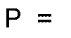

- Flexible circuits with heaters as set forth herein are capable of use to connect pad and pin grid arrays to p.c. boards or the like and to connect, for instance, 166 conductors in a 8.4 inch (213mm) wide circuit having the conductors at .05 inch (1.27mm) centres to a p.c. board or substrate in a surface mount configuration.
- The flexible circuit may be used to interconnect printed circuit boards, leaded and leadless chip carriers to printed circuit boards and printed circuit boards or the equivalent to multiple printed circuit boards. Further, the flexible circuit may be employed in a U-shaped configuration to contact exposed conductors on both sides of a daughter board and to contact conductors on a mother board all at the same time to provide a variety of selectable interconnections.
- In the various embodiments of the invention, use may be made of the advantages of the reliability, precise temperature control and relatively low temperature of the heaters, the solid connections provided by the solder and the flexibility of the circuits. Zero and low insertion force connectors are vastly improved since the solder imparts a very positive holding force at every contact point.
- Arrangements embodying the invention will now be described in more detail by way of example and with reference to the accompanying drawings, in which:-
- Figure 1 is a top view of a flexible circuit according to the present invention;
- Figure 1A is a top view of a variation of the arrangement of Figure 1;
- Figure 2 is a side view of the circuit of Figure 1;
- Figure 3 is a cross-sectional view of a heater incorporated in the circuit of Figure 1;
- Figure 4 is a detailed view of the heater terminal contact structure;
- Figure 5 is a pictorial view of a flexible circuit being soldered in place on a printed circuit board;
- Figure 5A is a side view in elevation of the combination of Figure 5;
- Figure 6 is a pictorial view of several uses of a flexible circuit according to the invention;
- Figure 7 is a sectional view of a daughter board support incorporating the heater-flexible circuit arrangement of the present invention;
- Figure 8 is a pictorial view of the device of Figure 7;
- Figure 9 is a view in section of a preferred form of heater;
- Figure 10 is a diagrammatic side view of an embodiment incorporating the heater of Figure 9;
- Figure 11 is a partly sectional side view of a pressure fit circuit board connector employing the present invention;
- Figure 12 is a perspective view of a flexible circuit of the present invention employed to connect a chip mounted on a leadless chip carrier to a printed circuit board;
- Figure 13 is a top view of the flexible circuit of Figure 12;
- Figure 14 is a view in elevation of part of the structure of Figure 12;
- Figure 15 is a perspective view of flexible circuits employed to connect multiple daughter boards.
- Figure 16 is a perspective view of a modification of the structure of Figure 12;
- Figure 17 is a perspective view of another form of heater for use with the flexible circuits of the present invention;
- Figure 18 is a perspective view of a structure according to the present invention employing a solder reflow pad;
- Figure 19 is a sectional view of the structure of Figure 18.
- Referring now specifically to Figures 1 and 2 of the accompanying drawings, there are illustrated two views of a flexible circuit with an integral heater. The flexible circuit, generally designated by the
reference numeral 2, has embedded in an insulatingflexible body 4, a plurality of conductors 6. The conductors 6 are illustrated for purposes of description only as a series of parallel conductors; it being understood that the conductors can conform to any desired pattern so long as, in the region where connection to an external or internal circuit or connector is to be made, they are arrayed in conformance with the circuit array of that other circuit or connector. This region is generally designated by the reference numeral 8. - In the region 8, the insulation covering the conductors 6 is removed and solder 10 or other heat activated conductive material is applied to the bared conductors 6. A
heater 12 lies across the region 8 of the flexible circuit, as viewed in Figure 2, being located on the opposite side of the circuit from the bared conductors 6. Theinsulation 4 in this embodiment is brought round to cover the heater and extends beyond the heater, where it is united to the main body of the flexible circuit. Thus the heater is sealed into thecircuit 2, at the region of the exposed conductors and solder, for heating the solder to its melt temperature and above to such extent as may be desired. - Referring to Figure 1A, an alternative layout of the heater structure is illustrated. A heater 5 is again laid across an end region of a
flexible circuit board 3 but instead of its end portion extending straight out of the edge of the flexible circuit as in Figure 1, it makes a 90° turn as at 7 and has a length 9 extending along a side edge of the circuit. Here current contact terminals 11 and 13 are provided; and in this embodiment agrommet 15 is passed through the opposite end of the heater remote from the terminals 11 and 13 to electrically connect the various layers together.Aligning holes 17 and 19 are provided in the corners of theboard 3. - Referring to Figure 3, the
heater 12 of Figure 1 is a self-regulating heater. A self-regulating heater of the type which may be employed herein includes aconductor 14 surrounded by athin layer 16 [.002" (.05mm) for instance] of theinsulation 4. Surrounding thelayer 16 is alayer 18 of ferromagnetic material about 1 to 1.8 skin depths thick, itself surrounded by a layer ofcopper 20. In its physical realisation, the heater illustrated may be 0.030 inch (0.76mm) thick, about 0.180 inch (4.6mm) wide, 9 inches (229mm) long and delivers about 250 watts of power at a temperature of 265°C: about the temperature of a wave solder machine. - As disclosed in US-A-4,256,945, if the heater is connected across a source of constant alternating current, the heater autoregulates at or approaching the Curie temperature of the ferromagnetic layer which in this application is, as indicated above, approximately 265°C. Connection to the
heater 12 is made atend location 22 of the heater (see Figure 4) where the copper-ferromagnetic outer layers are removed over an area to expose a region of theinsulation 16 and a smaller region of the insulation is removed to expose theconductor 14. The copper-ferromagnetic layers 20-18 on the one hand and thereturn conductor 14 on the other hand are connected together electrically at the end of the heater remote from theregion 22; that is, at the left end of the heater as viewed in Figure 1. This connection may be achieved simply by discontinuing the insulatinglayer 16 just short of the end of the heater remote fromregion 22 and compressing the end portion so that the conductors are all in contact; or the layers may be soldered together. - The
heater 12 is illustrated in Figure 1 as extending outwardly from theflexible circuit 2 but may well be terminated at the edge of thecircuit 2 with theregion 22 lying outwardly of the outermost conductor 6; or the heater contact area may lie along the side of the flexible circuit as in Figure 1A. - Referring now to Figures 5 and 5A of the accompanying drawings, there is illustrated, in pictorial view and side view, the connector region 8 of the
flexible circuit 2 of Figure 1 in alignment with a printedcircuit board 30 to which thecircuit 2 is to be connected. To insure alignment of the connector 8 of thecircuit 2 the connector 8 is provided withalignment holes 34 to mate withpins 32 on the printedcircuit board 30. - To connect the
conductors 42 of theflexible circuit 2 to the printedcircuit board 30, thepins 32 are aligned withholes 34 and the two boards are pressed together while current is applied to theheater 33 through ahole 44 in the upper surface of the circuit as viewed in Figures 5 and 5A. One of the important advantages of the arrangement is that the connections may be readily broken and remade a number of times thus greatly facilitating repair and maintenance. Asolder carrier pad 35, described in more detail below, may also be employed. - Another advantage of this type of connection is the ability to connect the flexible circuit to two or more distinct circuit boards. Reference is made now to Figure 6 of the accompanying drawings. A
flexible circuit 50 is provided at its two ends with heater and baredconductor arrangements leads circuit boards board 68, thus adding greatly to the architectural freedom of the physical layout of a piece of equipment. - Referring now to Figures 7 and 8 of the accompanying drawings, the
flexible circuit 50 of Figure 6 may be employed in a still further environment. A printedcircuit board 70 is to be connected to an interconnect board 72 via a zero insertion force connector 74 in the form of an elongated box open at the top and bottom. The body of the connector is composed of twoside walls walls flexible circuit 50 forms a "U" that has itslegs side walls base 88 extending across the open bottom of the connector 74. There may be three different heaters employed in this embodiment; two bonded to the upper ends of the legs of the "U" on the outer sides thereof. Athird heater 90 of the type described in Figure 3 lies on top of thebase portion 88 of theflexible circuit 50 and aresilient pad 92 is placed over the heater to hold it in position, to cushion the printed circuit board, and to provide mechanical compliance. - In this embodiment, the
board 70 has independent circuits on both its faces and each such circuit is to be connected independently to one or more circuits which may reside on the other side of theboard 70 or on the interconnect board 72. Connections between the two sides of the board are made by removal of the insulation from the two ends of the same conductor of the flexible circuit, while connection from one side or the other of theboard 70 to the interconnect board 72 is made by having an exposed conductor with solder along thebase 88 of the "U"-shaped flexible circuit which connects to the interconnect board through an aperture in the base of the flexible circuit. Thus, by simply selecting beforehand the areas of the conductors of the flexible circuit that are to be exposed, quite complex interconnection arrangements between multiple circuits are possible in addition to the primary printed circuit board-to-board connections. - In an example of various possible interconnections, the flexible circuit may interconnect a
conductor 94 on the left side of theboard 70 toconductor 96 on the right side of theboard 70, this approach being particularly useful with metal core boards where through-holes cannot be used. Continuing, aconductor 98 on the left side of theboard 70 may be connected to aconductor 100 on the interconnect board 72 and aconductor 102 on the right side ofboard 70 to aconductor 104 on the board 72, all as viewed in Figure 7. Power connection with the heaters may be made at thelocations - The scale of the drawings is not intended to be accurate; for example, the spacings between contacts on many of these types of contact structures is much closer than illustrated, the structures of Figures 1 and 7, for instance, having spacings of the order of only several mils (several quarters of a tenth of a millimetre) to a hundred mils (2.5mm). The conductors of the flexible structures can be as fine as those of the connectors or in some instances one conductor of a flexible circuit may bridge several conductors of a daughter board to assure contact, thereby reducing the required accuracy of the aligning structures. Alternatively, a contact of the flexible circuit may be made long enough to bridge two contacts of the
board 70, forinstance contacts - Referring now to Figure 9 of the accompanying drawings, there is illustrated a form of heater that may be employed as the
heater 90 of Figure 7. (Also see Figure 18). Theheater 90 illustrated in Figure 9 comprises aconductor 112, with alayer 114 of insulation (polyimide) surrounding and overlapped across the entire top of theconductor 112. The insulator is bonded on to the conductor with a suitable adhesive. The structure is enclosed by anouter layer 116 of copper having aninner lining 118 of ferromagnetic material. Thecopper layer 116 is also overlapped but does not require bonding since it will hold its bends. - The heater of Figure 9 may also be employed in the arrangement of Figure 10 which diagrammatically illustrates a different physical arrangement employing the heater and a flexible circuit.
Flexible circuit 120 is to be joined to a printedcircuit board 122 havingcontacts 124, only one of which is illustrated. The arrangement is similar to a large clothes peg or spring clip and employs aU-shaped spring 128 having afirst leg 130 secured to a first finger-engageable member 132. Asecond leg 134 of thespring 128 has theflexible circuit 120 bonded to an upper surface thereof as viewed in Figure 10, the flexible circuit being folded over the end ofleg 134 and extending under the leg. Aheater 136 is laminated into the flexible circuit and lies under theleg 134 and this assembly is situated such as to be in contact with the printedcircuit board 122. An L-shaped aligning pin 138 has its long leg secured to the top surface, as viewed in Figure 10, of the flexible circuit and itsshort leg 140 extending into analignment hole 142 in the printed circuit board. - By squeezing the members 132 and 138 together, the
leg 140 is raised and the structure may be applied to or, if already applied, withdrawn from the printedcircuit board 122. Thus the mechanism that provides the application and removal tool also provides for alignment of the two members. - Referring now specifically to Figure 11 of the accompanying drawings, there is illustrated in vertical section still another connector for printed circuit boards. This connector is a force fit type providing wiping of the contact areas upon insertion and withdrawal of the board. The drawing illustrates only the single heater case; the connector can have coplanar connection heaters as well as heaters and circuits on both sides of the board. A connector housing is composed of four main parts, a
flexible circuit clamp 146, a two-part flexible circuit containment member comprisingcontainment plates 148 and 150 and amain connector shell 152. Theshell 152 has anelongated base 154 having an upside down L-shapedmember 156 extending upwardly from the right edge thereof, as viewed in Figure 11. The base extends to the left of the L-shapedmember 156 to provide asurface 158 parallel to and spaced from thelower surface 160 of the horizontal top leg of the L-shapedmember 156. A generallytriangular spring 162 is positioned betweensurfaces apex 164 directed toward the left in Figure 11 and located about halfway betweensurfaces spring 162 is retained betweenside walls 166, only one of which is illustrated in Figure 11. - The
circuit containment plates 148 and 150 have the part 150 abutting against a left vertical surface 172 of theconnector shell 152. Theplate 148 has alower region 174 having a vertical surface 176 coextensive with surface 172.Upper region 178 ofmember 148 defines a space between itself and theflexible circuit clamp 146 in which aflexible circuit 180 is clamped between themembers flexible circuit 180 comes over the top of thecontainment plate 148 at about the level of the top leg of the L-shapedmember 156, and then descends downward in open space to pass opposite the apex 164 of thespring 162, subsequently passing between thecontainment plates 148 and 150 and out of the connector. The structure is held together bybolts 182 at opposite ends of thebase 154, the bolts passing in sequence throughmembers base 154. The flexiblecircuit containment plate 148 is recessed both opposite the apex 164 ofspring 162 and somewhat downwardly thereof to receiveheater 184 which may be separate from and bonded to or laminated in theflexible circuit 180. Theflexible circuit 180 has the insulation removed from its conductors inregion 185 opposite the apex of thespring 162 and has solder applied thereto. - In use, a
daughter board 186 is inserted by pressing it downwardly between thespring 162 and theflexible circuit 180. The spring causes theboard contact area 188 to be forced againstregion 185 of the flexible circuit as it is inserted thereby wiping the contact areas. The board comes to rest on thetop surface 190 of the containment plate 150, which extends betweenside walls 166 and serves as an alignment member for theboard 186 together with side walls not illustrated. The heater may now be energised to solder together the contact areas of the board and flexible circuit. - Another embodiment of the invention is intended to overcome a major problem encountered in placing leadless chip carriers on printed circuit boards. Due to different coefficients of thermal expansion and residual strains remaining after soldering a chip carrier to a board, solder joints fail and very expensive integrated circuits and/or boards may be lost. In addition, these devices often have a high failure rate and a connector such as disclosed herein that permits components to be readily removed and replaced is highly desirable. Referring specifically to Figure 12 of the accompanying drawings, there is illustrated a connector structure for relieving such problems.
- A
ceramic carrier 200 withleads 202 formed thereon, has achip 204 secured thereto in a conventional manner. The ceramic carrier has in its preferred embodiment as illustrated, a series of vertical, as viewed in Figure 12, castellations or recesses 206 formed therein. Eachcastellation 206, or other connection, intercepts adifferent lead 202 or several such leads and is filled with solder, gold or gold alloy for use at brazing temperatures. - Located between the
ceramic chip carrier 200 and a printed circuit board, or other appropriate circuit or circuit carrier, is a flexible circuit according to the present invention. The use of the flexible circuit permits the assembly to "move" with stress and temperature changes and thus greatly reduces failures in the solder due to cold working. Specifically, flexible circuit 208 (see also Figure 13) is of the same shape (square, rectangle, etc.) as the leadless chip carrier; a square is illustrated in Figure 13. A heater 210 following a square path but with the sides of the square lying at 45° to the sides of the flexible circuit, lies within the confines of the flexible circuit and intercepts the edges of the latter at their mid points. The flexible circuit has a plurality ofconductors 212 which are exposed where these align with the conductors on the board to which the chip is to be connected at terminals 214. Theconductors 212 are long enough to extend from terminals 214 lying under the heater, as illustrated in Figure 13, such that when the flexible circuit is folded over to cause the apices of the fourtriangles castellations 206, as seen in Figure 12. The pattern of conductors illustrated in Figure 13 is not the only pattern that can be employed, being determined by the pattern of conductors on the printed circuit board or other circuit to be contacted by the flexible circuit. - In use, the folded flexible circuit, which has solder or conductive adhesive applied to the exposed flexible circuit conductors, is laid on the printed circuit board, the leadless chip carrier is placed on the flexible circuit and the heater 210 is energised by applying a constant alternating current to
terminals 226 of the heater 210. Both sets of contacts are soldered together concurrently, or separately if desired, with the flexible circuit thereby connecting the printed circuit board and the chip carrier. If desired, the flexible circuit may be cut away in the region defined within the confines of the heater so that thecarrier 200 can be bonded to the board by epoxy or other suitable bonding agent. In addition to the advantages achieved by the use of the flexible circuit, strength is added to the structure by fillets ofsolder 228, see Figure 14, formed at the junction of the flexible circuit and thecarrier 200, which fillets in conjunction with the circuit traces in the flexible circuit and the solder in the castellations provide a long thin well-supported beam of solder and copper of relatively high strength, thus greatly increasing the ability of the system to tolerate the different coefficients of thermal expansion of the various elements of the system. Conductive adhesive which may be thermally actuated may also be employed in the castellations with perhaps some loss of strength in the beam. - Due to the great flexibility of flexible circuits, an arrangement such as illustrated in Figure 15 is possible. In such a structure a plurality of vertical, as viewed in the Figure, printed
circuit boards 230 are held in an upright position byholders 232. Aflexible circuit 234 extends from a printedcircuit board 236 into eachholder 232 passing between the sides and bottom of the holders and the sides and bottom of the boards adjacent a terminal end of each of theboards 230. At their upper ends, thecircuit boards 230 are held in proper spaced relationship by a grid-form holder 242 and a second flexible circuit 240 extends from a printedcircuit board 238 into contact with the faces of theboards 230 in similar fashion to theflexible circuit 234. Either theholders flexible circuits 234 and 240 may have the heaters formed thereon, depending upon preference. In each location where a connection is to be made the flexible circuit conductor is bared. It should be noted that the term flexible circuit as used herein is not limited to circuits as such but also includes flat cable, multiconductor flexible conductor straps such as are used to connect the movable heads of dot matrix printers to the print control circuits, and the like. - Referring specifically to Figure 16, there is illustrated a modification of the structure of Figure 12. A
ceramic chip carrier 258 has a chip attached thereto.Conductors 262 extend from chip contacts to solder filledcastellations 264. - A
flexible circuit 266 is secured to a printedcircuit board 268 and to thechip carrier 258 by a heat activated adhesive. The flexible circuit has a centrally locatedheater 270 and adhesive is applied to both its upper and lower surfaces as illustrated in Figure 16 so that when the flexible circuit is set on theboard 268 and the ceramic is set on the flexible circuit, the heater can be energised whereby the adhesive is activated and the elements become mechanically joined by thermal bonding. - The
flexible circuit 266 has asecond heater 272 which surrounds theheater 270 and is disposed over the bared and tinned ends, not illustrated, ofconductors 274, facing the printedcircuit board 268. Upon energisation of theheater 272 the ends of theconductors 274 are soldered to mating conductors on the printedcircuit board 268. - The
flexible circuit 266 is folded up along the edges of thechip carrier 258 so that tinned ends 276 ofconductors 274 are brought into contact with the solder in thecastellations 264. A heater is provided behind each group ofcontacts 276, these being designated bynumerals ends 276 ofconductors 274 to be soldered to the chip carrier so that a circuit for each lead 262 is completed through the solder ofcastellation 264,conductors 274 and through the terminals underheater 272 to the printedcircuit board 268. - The heater has been illustrated in two different forms in Figures 3 and 9. Another version of the heater is illustrated in Figure 17 of the accompanying drawings. A
flat copper bar 286, quite long but quite narrow, is coated on one surface with a layer offerromagnetic material 288. The copper bar is folded in half at 290 through a 180° angle so that the two halves of the bar are parallel to one another. Aninsulation layer 292 is disposed between the now juxtaposed regions of theferromagnetic layer 88. - This heater is quite thin and very effective; being of the order of 0.016 inch (0.4mm) thick.
- When soldering to very closely spaced leads, as small as .006 inch (0.15mm) between centres, a solder reflow pad may be required. Referring specifically to Figures 18 and 19 of the accompanying drawings, a heater, flexible circuit and reflow pad arrangement is illustrated. The heater consists of
buss 294,insulation layer 296,ferromagnetic layer 298 andouter copper layer 300.Flexible circuit 302 is folded around the heater and asolder reflow layer 304 overlies the exposed conductors of the flexible circuit. The solder reflow layer, which is secured to the flexible circuit in the region of the exposed conductors, is an insulating layer withwindows 306 filled withsolder 308. The spacing between windows corresponds to the spacing between conductors of the flexible circuit. The windows in the reflow layer confine the solder to the metal conductors and prevent short circuiting of the conductors. The reflow layer may alternatively be composed of two layers of insulating material with aligned windows with a continuous strip of solder in between the same. Either arrangement is acceptable. In cases where the surface is not regular a smooth elastomeric layer may be added for compliance and to maintain a relatively constant normal force across the contact area. - Some of the advantages of the flexible circuit of the invention now become readily apparent. The connection arrangement provides an unusually low profile; the contacts are, in effect, self soldering; very fine trace spacing, as little as .006" (.15mm), is currently possible; the heater is fully shielded and there are no long term creep problems, no contact resistance changes and no problems resulting from vibration; these features all being due to the self soldering capability of the flexible circuit. When using spacings of as little as .006" (.15mm), a reflow solder pad, such as illustrated in Figure 18, is preferably employed.
- Another interesting advantage of the use of a flexible circuit with heater relates to avoiding corrosion and/or oxidation of the exposed solder and contacts during shipping and storage of the circuits. As a result of the availability of a heat source applying heat uniformly to all solder-conductor regions, the circuit may be bonded to a metallic plate for storage and shipping, thus excluding air and moisture from contact areas. When it is desired to use the circuit, the heater is energised so that the board can be removed from the metallic plate, leaving clean exposed solder surfaces.
- Although reference is made throughout to solder as the heat sensitive bonding material, other heat sensitive, conductive, bonding materials may be employed. Such other materials may include conductive thermosetting and thermoplastic resins; and the term "solder" includes liquid solders, and gold and silver solders, all of which may be employed in various of the embodiments.
- The term "constant current" as employed herein does not mean a current that cannot increase but means a current that obeys the following formula

Specifically, in order to autoregulate, the power delivered to the load when the heater exceeds Curie temperature must be less than the power delivered to the load below Curie temperature. If the current is held invariable, then the best autoregulating ratio is achieved short of controlling the power supply to reduce current. So long, however, as the current is reduced sufficiently to reduce heating, autoregulation is achieved. Thus when large autoregulating ratios are not required, constraints on the degree of current control may be relaxed thereby reducing the cost of the power supply. - The above equation is derived by analysing the equation:

where P is power.
Differentiating P with respect to R

and to satisfy the requirements for autoregulation

Thus,

which reduces to Equation 1 above.
Claims (22)
- An electrical circuit assembly for connection to other circuits, comprising one or more electrical conductors embedded in and covered by a body of insulating material having two large opposed surfaces, said conductor or each conductor having a connection region where it is exposed at one of said opposed surfaces, characterised in that the body of insulating material (4) containing the embedded conductor or conductors (6) is flexible and a self-regulating electrical resistance heater (12) to apply heat for making electrical connection, especially soldered connection, and adapted to be energised from a source of substantially constant a.c. current is disposed along the other of said opposed surfaces at the region opposite that where said conductor or conductors are exposed.
- An assembly according to Claim 1, wherein said exposed surface (10) of said conductor or each conductor is covered with solder.
- An assembly according to Claim 1 or Claim 2, wherein said body of insulating material is in the form of a flexible board or strap and has a multiplicity of conductors embedded in it a plurality of which are exposed at the connection region in a predetermined array, and the heater is elongated to extend along said array but on the opposite surface of the board or strap.
- An assembly according to Claim 3, further including a solder carrier pad (35) of insulating material which overlies said array of exposed portions of the conductors and has a series of apertures in alignment with said exposed portions which are filled with solder.
- An assembly according to Claim 4, wherein the solder carrier pad has a compliant insulating layer generally coextensive with the pad.
- An assembly according to any of Claims 3 to 5, wherein said body of insulating material has a flap extending beyond the connection region which contains no conductors and is folded back over the heater to cover it.
- An assembly according to any preceding claim, wherein said heater is of the order of .76 mm thick.
- An assembly according to any of Claims 3 to 6, further including a second electrical circuit for connection to said flexible circuit board and having a pattern of conductors with an array of exposed portions generally the same as the array of exposed portions of the conductors of the flexible circuit, with means for aligning said two arrays when the circuits are brought together for connection.
- An assembly according to any of claims 3 to 6, wherein said flexible circuit has a plurality of different connection regions at each of which there is a different array of exposed portions of the conductors along one surface, with a respective heater lying opposite the array along the other surface of the flexible circuit, and further including a respective plurality of other electrical circuits each having electrical conductors with an array of exposed portions generally the same as a respective one of the arrays of exposed portions of the flexible circuit, with means for aligning each of the arrays of exposed conductor portions of the flexible circuit with the array of exposed conductor portions of the respective other circuit when the circuits are assembled together.
- An assembly according to any of Claims 3 to 6, including an electrical connector for connection to said flexible circuit board and having a plurality of alternating bands of insulating material and conductive material, said bands of conductive material having a spacing and pattern corresponding to said exposed portions of the conductors of the flexible circuit, with means for aligning said bands of conductive material and said exposed conductor portions for connection of respective conductive bands to respective flexible circuit conductors.
- An assembly according to any of Claims 8 to 10, wherein said aligning means comprises at least one holder having at least one opening within which the flexible circuit is constrained to lie, a separate circuit board also being accommodated in the same opening for contact with the flexible circuit.
- An assembly according to Claim 11, wherein the holder is generally U-shaped and the flexible circuit is constrained to adopt substantially a U-configuration within the holder, the separate circuit board being inserted between the legs of the U.
- An assembly according to Claim 11, wherein the holder is generally in the form of an elongated box open at the top and bottom, the flexible circuit is constrained to adopt substantially a U-configuration within the box, the separate circuit board being inserted between the sides of the box, and a further separate circuit board or connector lies across the open bottom of the box in contact with the base of the U.
- An assembly according to Claim 11, wherein the holder incorporates spring means for spring-pressing the separate circuit board against the flexible circuit.
- An assembly according to Claim 14, wherein the holder is generally in the form of a spring clip to grip a marginal portion of the separate circuit board, with location means for locating the clip-like holder in correct position on said board.
- An assembly according to any of Claims 3 to 6, including a separate circuit board and an insulating mount secured thereon and carrying a further electronic component, the flexible circuit being interposed between the mount and the circuit board to connect terminals of the electronic component to conductors on the circuit board.
- An assembly according to Claim 16, wherein the flexible circuit is folded up to enable conductors of the flexible circuit to reach the terminals of the component on the mount.
- An assembly according to Claim 16 or Claim 17, wherein the mount has castellations or recesses around its sides containing terminals of the component on the mount and solder.
- An assembly according to any of Claims 16 to 18, wherein the flexible circuit is provided with a first self-regulating heater or group of such heaters for soldering the electrical connections and a further heater for activating a heat-activatable bonding material to bond the mount and the flexible circuit to the circuit board.
- An assembly according to any of Claims 16 to 18, wherein the flexible circuit is of square configuration, the self-regulating heater follows a path having the configuration of a smaller square within the confines of the larger square defining the flexible circuit, the smaller square having its sides at 45° with respect to the sides of the larger square, and the four corners of the square flexible circuit are folded in to meet at the centre of the squares.
- A method of making multiple electrical circuit connections, such as in the connecting together of electrical circuit boards, wherein a first array of exposed portions of otherwise insulated electrical conductors embedded in a circuit board are soldered to a co-operating second array of exposed portions of conductors of another circuit assembly by the application of heat to melt the solder, characterised in that said first array of conductor portions is exposed at one surface of a circuit board made of a flexible insulating material and, after the two arrays of exposed conductor portions have been brought together in assembled alignment and solder has been supplied to their contact surfaces, the heat to melt the solder is generated by a self-regulating electrical resistance heater energised by a substantially constant a.c. current which heater is applied to the other surface of the flexible circuit board opposite to said first array of exposed conductor portions.
- The method according to Claim 21, wherein prior to assembly of said two arrays of exposed conductor portions, the conductor portions of the flexible circuit board are protected by a cover plate soldered thereto which cover plate is released for removal to expose said conductor portions in readiness for assembly by energising said heater to fuse the solder.
Priority Applications (1)
| Application Number | Priority Date | Filing Date | Title |
|---|---|---|---|
| AT86304393T ATE84928T1 (en) | 1985-06-20 | 1986-06-09 | SELF-DEPLACHABLE FLEXIBLE CONNECTION. |
Applications Claiming Priority (2)
| Application Number | Priority Date | Filing Date | Title |
|---|---|---|---|
| US746796 | 1985-06-20 | ||
| US06/746,796 US4788404A (en) | 1985-06-20 | 1985-06-20 | Self-soldering flexible circuit connector |
Publications (3)
| Publication Number | Publication Date |
|---|---|
| EP0206619A2 EP0206619A2 (en) | 1986-12-30 |
| EP0206619A3 EP0206619A3 (en) | 1988-10-26 |
| EP0206619B1 true EP0206619B1 (en) | 1993-01-20 |
Family
ID=25002368
Family Applications (1)
| Application Number | Title | Priority Date | Filing Date |
|---|---|---|---|
| EP86304393A Expired - Lifetime EP0206619B1 (en) | 1985-06-20 | 1986-06-09 | Self-soldering, flexible circuit connector |
Country Status (6)
| Country | Link |
|---|---|
| US (1) | US4788404A (en) |
| EP (1) | EP0206619B1 (en) |
| JP (1) | JPS61294778A (en) |
| AT (1) | ATE84928T1 (en) |
| CA (1) | CA1255012A (en) |
| DE (1) | DE3687546T2 (en) |
Cited By (1)
| Publication number | Priority date | Publication date | Assignee | Title |
|---|---|---|---|---|
| DE19540140B4 (en) * | 1995-10-27 | 2006-08-24 | Coherent Lübeck GmbH | Substrate, module and method for mounting components of the module on the substrate |
Families Citing this family (24)
| Publication number | Priority date | Publication date | Assignee | Title |
|---|---|---|---|---|
| JPS6466990A (en) * | 1987-09-08 | 1989-03-13 | Furukawa Electric Co Ltd | Molded circuit board |
| US5093545A (en) * | 1988-09-09 | 1992-03-03 | Metcal, Inc. | Method, system and composition for soldering by induction heating |
| FR2638050B1 (en) * | 1988-10-18 | 1996-03-01 | Thomson Hybrides | COMPONENT TRANSFER DEVICE ON A HYBRID CIRCUIT |
| US5059756A (en) * | 1988-11-29 | 1991-10-22 | Amp Incorporated | Self regulating temperature heater with thermally conductive extensions |
| US5065501A (en) * | 1988-11-29 | 1991-11-19 | Amp Incorporated | Generating electromagnetic fields in a self regulating temperature heater by positioning of a current return bus |
| US5010233A (en) * | 1988-11-29 | 1991-04-23 | Amp Incorporated | Self regulating temperature heater as an integral part of a printed circuit board |
| US4990736A (en) * | 1988-11-29 | 1991-02-05 | Amp Incorporated | Generating electromagnetic fields in a self regulating temperature heater by positioning of a current return bus |
| US5032703A (en) * | 1988-11-29 | 1991-07-16 | Amp Incorporated | Self regulating temperature heater carrier strip |
| US5103071A (en) * | 1988-11-29 | 1992-04-07 | Amp Incorporated | Surface mount technology breakaway self regulating temperature heater |
| JPH0319389A (en) * | 1989-06-16 | 1991-01-28 | Fujitsu Ltd | Printed circuit board |
| US5004887A (en) * | 1989-07-24 | 1991-04-02 | Amp Incorporated | Heating apparatus having Curie effect heater |
| US5007574A (en) * | 1989-09-14 | 1991-04-16 | Metcal, Inc. | Desoldering device |
| FR2657220B1 (en) * | 1990-01-12 | 1993-11-05 | Thomson Csf | PRINTED CIRCUIT FOR THE SUPPORT AND INTERCONNECTION OF ELECTRONIC COMPONENTS, INCLUDING A SOLDERING DEVICE. |
| US5260548A (en) * | 1990-02-23 | 1993-11-09 | Toddco General, Inc. | Soldering system controlled power supply apparatus and method of using same |
| US5182427A (en) * | 1990-09-20 | 1993-01-26 | Metcal, Inc. | Self-regulating heater utilizing ferrite-type body |
| US5539186A (en) * | 1992-12-09 | 1996-07-23 | International Business Machines Corporation | Temperature controlled multi-layer module |
| US5568892A (en) * | 1994-06-16 | 1996-10-29 | Lucent Technologies Inc. | Alignment and bonding techniques |
| EP1097797B1 (en) * | 1999-11-02 | 2004-02-04 | TOHOKU MUNEKATA Co., Ltd. | Joining thermoplastic cases and covers by fusion |
| US6423939B1 (en) * | 2000-10-02 | 2002-07-23 | Agilent Technologies, Inc. | Micro soldering method and apparatus |
| US6870251B2 (en) * | 2002-05-29 | 2005-03-22 | Intel Corporation | High-power LGA socket |
| US6710303B1 (en) * | 2002-11-13 | 2004-03-23 | W.E.T. Automotive Systems Ag | Intermediate electrical connecting device for seat-heating systems |
| US20040112935A1 (en) * | 2002-12-16 | 2004-06-17 | Visteon Global Technologies, Inc. | Integrated flex substrate metallurgical bonding |
| FR2912029B1 (en) * | 2007-01-31 | 2010-10-22 | Hispano Suiza Sa | ELECTRONIC BOARD INCORPORATING A HEATING RESISTANCE. |
| KR102194717B1 (en) * | 2015-01-06 | 2020-12-23 | 삼성전기주식회사 | Printed circuit board and method of manufacturing the same |
Family Cites Families (6)
| Publication number | Priority date | Publication date | Assignee | Title |
|---|---|---|---|---|
| FR2424646A1 (en) * | 1978-04-28 | 1979-11-23 | Commissariat Energie Atomique | CONNECTION PROCESS OF CONNECTION TERMINALS OF ELECTRICAL ASSEMBLIES |
| DE2939922C2 (en) * | 1978-10-12 | 1983-03-17 | International Computers Ltd., London | Electrical cable connector assembly |
| JPS5936540B2 (en) * | 1980-05-15 | 1984-09-04 | 敬一郎 長谷川 | Preservation and disinfection equipment for cultural properties, etc. |
| JPS5811115A (en) * | 1981-07-13 | 1983-01-21 | Asahi Fiber Glass Co Ltd | Manufacture for frp with rib |
| GB2127740B (en) * | 1982-09-30 | 1985-10-23 | Burr Brown Res Corp | Improved hermetic sealing process |
| GB2134026B (en) * | 1983-01-27 | 1985-11-20 | Allen Bradley Int | A method of joining a component part to an integrated circuit |
-
1985
- 1985-06-20 US US06/746,796 patent/US4788404A/en not_active Expired - Lifetime
-
1986
- 1986-05-26 CA CA000510002A patent/CA1255012A/en not_active Expired
- 1986-06-09 EP EP86304393A patent/EP0206619B1/en not_active Expired - Lifetime
- 1986-06-09 DE DE8686304393T patent/DE3687546T2/en not_active Expired - Fee Related
- 1986-06-09 AT AT86304393T patent/ATE84928T1/en not_active IP Right Cessation
- 1986-06-20 JP JP61145977A patent/JPS61294778A/en active Pending
Non-Patent Citations (1)
| Title |
|---|
| IBM TECHNICAL DISCLOSURE BULLETIN, vol. 9, no. 11, April 1967, page 1688, New York, US; T.L. PALFI et al.: "Selective electrical heater system for module removal". * |
Cited By (1)
| Publication number | Priority date | Publication date | Assignee | Title |
|---|---|---|---|---|
| DE19540140B4 (en) * | 1995-10-27 | 2006-08-24 | Coherent Lübeck GmbH | Substrate, module and method for mounting components of the module on the substrate |
Also Published As
| Publication number | Publication date |
|---|---|
| JPS61294778A (en) | 1986-12-25 |
| CA1255012A (en) | 1989-05-30 |
| EP0206619A3 (en) | 1988-10-26 |
| DE3687546T2 (en) | 1993-06-03 |
| US4788404A (en) | 1988-11-29 |
| EP0206619A2 (en) | 1986-12-30 |
| DE3687546D1 (en) | 1993-03-04 |
| ATE84928T1 (en) | 1993-02-15 |
Similar Documents
| Publication | Publication Date | Title |
|---|---|---|
| US4788404A (en) | Self-soldering flexible circuit connector | |
| US5175409A (en) | Self-soldering flexible circuit connector | |
| US4894015A (en) | Flexible circuit interconnector and method of assembly thereof | |
| US4827611A (en) | Compliant S-leads for chip carriers | |
| US5210939A (en) | Lead grid array integrated circuit | |
| US5129573A (en) | Method for attaching through-hole devices to a circuit board using solder paste | |
| JP2664873B2 (en) | Electronic package and manufacturing method thereof | |
| KR0141067B1 (en) | Electronic package with thermally conductive support member to which thin circuit board and semiconductor device are bonded | |
| JPH07263092A (en) | Electrical assembly and method of making an electrical connection between an electrical component and a circuit board | |
| US4554575A (en) | Low stress leadless chip carrier and method of assembly | |
| JPH0661606A (en) | Circuit package structure | |
| JPH0773152B2 (en) | Electronic package and method of making the same | |
| US4952529A (en) | Method of coupling a terminal to a thick film circuit board | |
| US6902097B2 (en) | Electrically conductive wire | |
| GB2105120A (en) | Electrical programmable plug | |
| KR100592137B1 (en) | Method of mounting electronic parts and electronic circuit device manufactured by the method | |
| US8902605B2 (en) | Adapter for plated through hole mounting of surface mount component | |
| JP2991155B2 (en) | Electronic components and their mounting structures | |
| US5288959A (en) | Device for electrically interconnecting opposed contact arrays | |
| US6281449B1 (en) | Printed board, manufacturing method therefor and structure for connecting conductor elements to the printed board | |
| US5045666A (en) | Self-soldering flexible circuit connector | |
| EP0685990B1 (en) | Apparatus for mounting electrical devices to a circuit board | |
| JP3297708B2 (en) | connector | |
| US6132226A (en) | Structure and method for mounting an electronic part | |
| JPH0634446B2 (en) | Circuit board soldering method |
Legal Events
| Date | Code | Title | Description |
|---|---|---|---|
| PUAI | Public reference made under article 153(3) epc to a published international application that has entered the european phase |
Free format text: ORIGINAL CODE: 0009012 |
|
| AK | Designated contracting states |
Kind code of ref document: A2 Designated state(s): AT BE CH DE FR GB IT LI NL SE |
|
| RHK1 | Main classification (correction) |
Ipc: H05K 3/34 |
|
| PUAL | Search report despatched |
Free format text: ORIGINAL CODE: 0009013 |
|
| AK | Designated contracting states |
Kind code of ref document: A3 Designated state(s): AT BE CH DE FR GB IT LI NL SE |
|
| 17P | Request for examination filed |
Effective date: 19890317 |
|
| 17Q | First examination report despatched |
Effective date: 19901031 |
|
| GRAA | (expected) grant |
Free format text: ORIGINAL CODE: 0009210 |
|
| AK | Designated contracting states |
Kind code of ref document: B1 Designated state(s): AT BE CH DE FR GB IT LI NL SE |
|
| PG25 | Lapsed in a contracting state [announced via postgrant information from national office to epo] |
Ref country code: LI Effective date: 19930120 Ref country code: SE Effective date: 19930120 Ref country code: AT Effective date: 19930120 Ref country code: NL Effective date: 19930120 Ref country code: CH Effective date: 19930120 Ref country code: BE Effective date: 19930120 Ref country code: IT Free format text: LAPSE BECAUSE OF FAILURE TO SUBMIT A TRANSLATION OF THE DESCRIPTION OR TO PAY THE FEE WITHIN THE PRESCRIBED TIME-LIMIT;WARNING: LAPSES OF ITALIAN PATENTS WITH EFFECTIVE DATE BEFORE 2007 MAY HAVE OCCURRED AT ANY TIME BEFORE 2007. THE CORRECT EFFECTIVE DATE MAY BE DIFFERENT FROM THE ONE RECORDED. Effective date: 19930120 |
|
| REF | Corresponds to: |
Ref document number: 84928 Country of ref document: AT Date of ref document: 19930215 Kind code of ref document: T |
|
| REF | Corresponds to: |
Ref document number: 3687546 Country of ref document: DE Date of ref document: 19930304 |
|
| REG | Reference to a national code |
Ref country code: CH Ref legal event code: PL |
|
| ET | Fr: translation filed | ||
| NLV1 | Nl: lapsed or annulled due to failure to fulfill the requirements of art. 29p and 29m of the patents act | ||
| PLBE | No opposition filed within time limit |
Free format text: ORIGINAL CODE: 0009261 |
|
| STAA | Information on the status of an ep patent application or granted ep patent |
Free format text: STATUS: NO OPPOSITION FILED WITHIN TIME LIMIT |
|
| 26N | No opposition filed | ||
| PGFP | Annual fee paid to national office [announced via postgrant information from national office to epo] |
Ref country code: GB Payment date: 19980609 Year of fee payment: 13 |
|
| PGFP | Annual fee paid to national office [announced via postgrant information from national office to epo] |
Ref country code: DE Payment date: 19980612 Year of fee payment: 13 |
|
| PGFP | Annual fee paid to national office [announced via postgrant information from national office to epo] |
Ref country code: FR Payment date: 19980625 Year of fee payment: 13 |
|
| PG25 | Lapsed in a contracting state [announced via postgrant information from national office to epo] |
Ref country code: GB Free format text: LAPSE BECAUSE OF NON-PAYMENT OF DUE FEES Effective date: 19990609 |
|
| PG25 | Lapsed in a contracting state [announced via postgrant information from national office to epo] |
Ref country code: FR Free format text: THE PATENT HAS BEEN ANNULLED BY A DECISION OF A NATIONAL AUTHORITY Effective date: 19990630 |
|
| GBPC | Gb: european patent ceased through non-payment of renewal fee |
Effective date: 19990609 |
|
| PG25 | Lapsed in a contracting state [announced via postgrant information from national office to epo] |
Ref country code: DE Free format text: LAPSE BECAUSE OF NON-PAYMENT OF DUE FEES Effective date: 20000503 |
|
| REG | Reference to a national code |
Ref country code: FR Ref legal event code: ST |