EP0198568A2 - Data capture logic system - Google Patents
Data capture logic system Download PDFInfo
- Publication number
- EP0198568A2 EP0198568A2 EP86300144A EP86300144A EP0198568A2 EP 0198568 A2 EP0198568 A2 EP 0198568A2 EP 86300144 A EP86300144 A EP 86300144A EP 86300144 A EP86300144 A EP 86300144A EP 0198568 A2 EP0198568 A2 EP 0198568A2
- Authority
- EP
- European Patent Office
- Prior art keywords
- data
- capture
- register
- control
- data capture
- Prior art date
- Legal status (The legal status is an assumption and is not a legal conclusion. Google has not performed a legal analysis and makes no representation as to the accuracy of the status listed.)
- Withdrawn
Links
- 238000013481 data capture Methods 0.000 title claims abstract description 148
- 230000006870 function Effects 0.000 claims abstract description 40
- 238000012360 testing method Methods 0.000 claims abstract description 23
- 238000001514 detection method Methods 0.000 claims abstract description 16
- 230000004044 response Effects 0.000 claims description 3
- 238000013461 design Methods 0.000 description 15
- 238000004458 analytical method Methods 0.000 description 9
- 238000000034 method Methods 0.000 description 9
- 238000003491 array Methods 0.000 description 4
- 238000012545 processing Methods 0.000 description 4
- 230000009467 reduction Effects 0.000 description 4
- 230000008569 process Effects 0.000 description 3
- 230000008901 benefit Effects 0.000 description 2
- 230000003111 delayed effect Effects 0.000 description 2
- 238000011161 development Methods 0.000 description 1
- 238000003745 diagnosis Methods 0.000 description 1
- 230000006872 improvement Effects 0.000 description 1
- 238000007689 inspection Methods 0.000 description 1
- 238000002955 isolation Methods 0.000 description 1
- 238000012423 maintenance Methods 0.000 description 1
- 230000000873 masking effect Effects 0.000 description 1
- 230000007246 mechanism Effects 0.000 description 1
- 239000007787 solid Substances 0.000 description 1
- 230000001960 triggered effect Effects 0.000 description 1
Images

Classifications
-
- G—PHYSICS
- G01—MEASURING; TESTING
- G01R—MEASURING ELECTRIC VARIABLES; MEASURING MAGNETIC VARIABLES
- G01R31/00—Arrangements for testing electric properties; Arrangements for locating electric faults; Arrangements for electrical testing characterised by what is being tested not provided for elsewhere
- G01R31/28—Testing of electronic circuits, e.g. by signal tracer
- G01R31/317—Testing of digital circuits
- G01R31/3181—Functional testing
- G01R31/3185—Reconfiguring for testing, e.g. LSSD, partitioning
- G01R31/318533—Reconfiguring for testing, e.g. LSSD, partitioning using scanning techniques, e.g. LSSD, Boundary Scan, JTAG
- G01R31/318566—Comparators; Diagnosing the device under test
-
- G—PHYSICS
- G06—COMPUTING; CALCULATING OR COUNTING
- G06F—ELECTRIC DIGITAL DATA PROCESSING
- G06F11/00—Error detection; Error correction; Monitoring
- G06F11/30—Monitoring
- G06F11/34—Recording or statistical evaluation of computer activity, e.g. of down time, of input/output operation ; Recording or statistical evaluation of user activity, e.g. usability assessment
Definitions
- This invention relates to data capture logic systems for use with very large scale integrated circuit chips, also known as VLSI chips, for example, to provide test and error checking functions in addition to the operational functions of the chip.
- a data capture logic system according to the present invention may be located on a VLSI chip and programmed to store certain operands from a VLSI logic function circuit during operation, as well as storing operands at different time cycles during operation so that the functioning of the circuit may be analysed.
- the present invention has particular application to VLSI chips that have a pipeline or pipe sequence of operations.
- Such "weak" areas may have poor tolerance or margins to voltage fluctuation, timing variations or other factors. Therefore, it is important in VLSI logic design to create an internal system which can test or sample preselected, important data points internal to the logic structure. Because some errors are intermittent and do not occur under all conditions, but only under certain conditions, it is especially difficult to diagnose these errors in large systems. Diagnosis of intermittent errors can be especially aided if the failing input data at various positions internal to a logic circuit can be captured along with the input operands to the logic structure.
- VLSI logic chip arrays are limited in number and primarily used for operational purposes, tests for error function logic must be allowed to take only a very small number of the input and output pins that can be placed on a VLSI chip.
- VLSI logic design and error functions One known technique for analysing VLSI logic design and error functions is known as the level sensitive scan design in which a substantial number of registers are combined with the logic system on a VLSI chip so that on demand the contents of all of the registers may be delivered in a continuous serial fashion to an output pin of the chip.
- This system requires the stringing together of a significant number of operand registers in the VLSI chip in order to output a substantial body of serial data. All of this data is captured at the same time and represents a burden to analyse all of the particular operands and unnecessary information captured by this method. Also, this method does not capture the correct input operands to correlate with operands in various processing steps.
- this duplication of logic may be necessary in some applications, it should not be necessary for all applications. Also, this duplicate logic system may show that an error is occurring internal to a logic system, but does not help determine the type of error that is occurring by capturing both input and failing output operands from the same internal function.
- US-A-4357703 shows that certain test functions could be performed with LSI logic and that input and output operands could be captured in parallel fashion in registers for serial shifting into and out of the chip for test purposes.
- This system was good for LSI level logic design but VLSI demands other techniques because of the high logic density on a chip.
- US-A-4357703 does not show a system for capturing data operands internally in the VLSI logic structure at different times during functioning of the VLSI logic.
- a data capture logic system to be associated with a VLSI logic array having a plurality of data registers characterised by comprising: a control register for holding various input data representing control functions for data capture mode logic; a plurality of data capture registers, each of which is connectable to one of the data registers in said logic array holding a selected operand from the logic array under test and responsive to a control function, wherein said data capture.
- registers are connected to receive control signals from said control register; a plurality of error detection means located in said logic array under test which will detect errors in operands occurring in the VLSI logic array under test; means responsive to said error detection means and connected to said data capture registers to store data in said data capture registers when an error is detected; and an output data capture register connected to said data capture registers and having a control portion and a data operand portion wherein said control portion holds control signals representative of an indication of the type of data failure which has occurred and wherein said data operand portion is arranged to control selected failed data operands received from said data capture registers.
- the data capture logic system may include a soft memory connectable to one of the input registers for holding predetermined values of operands for determining the data capture functions to be performed, and a capture mode select and delay device connected to receive signals from said soft control memory and from said control register and connected to at least one of said data capture registers so that predetermined operands can be captured at preselected times.
- the data capture logic system preferably includes at least one multiplex data capture register which can select possible capture operands from a plurality of data registers, and select network means associated with the or each said multiplex data capture register for controlling which data operand is selected for capture, said select network means being connected to and responsive to said control register, said capture mode select and delay device and said error detection means for selecting which operand is to be captured by the associated multiplex data capture register.
- Said control register may have means for storing a selection override enable signal and at least one multiplex data capture register being connected to receive more than one data operand and connected to said control register to receive said override enable signal so that said multiplex data capture register can be controlled to capture a different data operand from a different data register than would normally be captured.
- said control register may have means for storing a selected override value signal, at least one multiplex data capture register being connected to receive more than one data operand and a select network connected to said control register to receive said selection override value signal so that said multiplex data capture register is responsive to said select network to capture a different data operand in response to said preselected value from a different data register than would normally be captured.
- the data capture logic system comprises means for producing an output hold source signal indicative of an error in input operand so that a device preceding the VLSI logic array can capture data.
- the data capture logic system may include hold source control means for receiving an input hold source control signal indicative of an output operand error, said hold source control means connected to said output data capture register to cause said output data capture register to capture data operands.
- Said data capture logic system may include a capture mode select and delay device connected to receive signals from said control register and connected to control at least one of said data capture registers, said control register having means for storing a capture delay select control signal for controlling said capture mode select and delay device to cause said at least one of said data capture registers to capture data operands at a preselected time different from the time at which other of said data capture registers capture data operands.
- a soft control memory is connectable to one of the data registers for holding predetermined values of data operands for determining the data capture functions to be performed, said soft control memory being connected to con- trot said capture mode select and delay device.
- a data capture logic system to be associated with a VLSI logic array comprising: a plurality of logic error detection circuits connected to data registers in said logic array and in operation producing output logic error signals when an error occurs; a control register for holding various input data representing control functions for the data capture logic system; a soft control memory which holds predetermined values for determining the time of a data capture function to be performed in the event of a detected error and selected time of a data capture function when no error is detected; a capture mode select and delay device connected to receive signals from said soft control memory and from one of the data registers to determine a forced data capture when no error is detected; a plurality of data capture stages, each of which has one or more registers for holding selected operands from the logic array under test and selected control status flags, said registers, in operation, receiving control signals from said data registers, said soft control memory, said capture mode select and delay device, and said logic error detection circuits; multiplexer control means for selecting which oper
- Said logic error detection circuit may be parity check circuits.
- Said control register may have means for storing a selection override enable signal, at least one multiplex data capture register veing connected to receive more than one data operand and connected to said control register to receive said override enable signal so that said multiplex data capture register can be controlled to capture a different data operand from a different data register than would normally be captured.
- said control register may have means for storing a selection override value signal and further comprising at least one multiplex data capture register connected to receive more than one data operand and a select network connected to said control register to receive said override enable signal so that said multiplex data capture register is responsive to said select network to capture a different data operand in reponse to said preselected value from a different data register than would normally be captured.
- the data capture logic system may include means for producing an output hold source signal indicative of an error in input operands so that a device preceding the VLSI logic array can capture data.
- a data capture logic system may include hold source control means for receiving an input hold source control signal indicative of an output operand error, said hold source control means being connected to said output data capture operand register to cause said output data capture register to capture data operands.
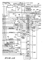
- Figures 1A and 1 B which, when viewed in left to right order, are a schematic drawing of a logic circuit together with a data capture logic system according to the present invention.
- FIG. 1A and 1B a combined VLSI logic array and data capture logic system 10 according to the present invention is shown.
- the VLSI logic array does not form a part of the present invention but the data capture logic system according to the present invention can only be shown in connection with such a VLSI logic array.
- a sample gate logic array 11 is shown within dotted lines. The array 11 contains a pipe structure of sequenced operations.
- An "A" operand is inputted in parallel through a channel 12 to a register 14.
- a "B” operand is inputted in parallel through a channel 16 to a register 18.
- a control operand is provided through a data channel 20 to a register 22.
- Each of the parity check circuits is connected respectively to a logic circuit 30 and to a register 32, the operation of which will be explained later.
- the register 14 has an output connected to an input of an adder 34.
- the register 18 has an output which is connected as the other input to the adder 34.
- the output of the adder 34 is the sum of the "A" and the "B" operand which is connected to a register 36.
- the register 36 has an associated parity check circuit 38 which has an output connected to additional circuits, as will be explained later.
- the output of the register 36 is connected to an additional combinational logic circuit 40, which is part of the VLSI logic array.
- the combinational logic circuit 40 performs additional operations on operands it receives.
- the register 22 is connected to a soft control memory 42, which stores the control operands it receives.
- the output of the soft control memory 42 is connected to a register 44, which also has an associated parity check circuit 46.
- the output of the register 44 is connected as an input to the combinational logic circuit 40.
- the output of the soft control memory 42 is also connected with a capture mode select and delay logic circuit 50 which is part of the data capture logic circuit of the present invention as will be described later.
- the output result of the combinational logic circuit 40 is connected to a multiplexer register 52 which selects inputs from different sources.
- One input to the register 52 is indicated schematically as a constant on a data line 54. This constant might be all binary 1's or all binary 0's, or some other appropriate constant, for use with the circuit.
- the control for the register 52 is provided on a data channel 56 from the output of the register 44.
- the register 52 also has an associated parity check circuit 58.
- the output of the register 52 is provided as an output to the logic array 11 on a data channel 60, which represents the results of the operations performed on the input operands.
- the capture mode select and delay logic circuit 50 is an optional system for controlling the time of data capture.
- the soft control memory 42 has an input line to the circuit 50, which can provide a capture signal to provide a capture of particular data at a predetermined time.
- an external capture signal can be provided on a data channel 70 to control a particular capture of data from outside of the system.
- the specific data capture trigger is selected by a channel 80 and the additional delay factor is selected by a channel 82.
- An input register system with its controls is shown generally within a dotted line box 72.
- This input register system consists of a register having various sections into which data is serially shifted and from which data may be removed in parallel to drive various portions of the data capture logic system according to the present invention.
- the first two sections of a control register 74 are a section 76 containing the capture mode select logic and a section 78 containing the capture delay select logic.
- the section 76 provides a capture mode select signal on the channel 80 to the capture mode select and delay circuit 50 and the section 78 provides a signal on the channel 82 to the capture mode select and delay logic 50.
- the output of the capture mode select and delay logic circuit 50 is connected to a register 84 and provides a control signal to capture data.
- the output of the register 84 is passed on to a register 86.
- the logic circuit 30 is an OR gate which receives inputs from the parity check circuits 24, 26, 28. If any one of the input registers 14, 18, 22 shows an input parity error then the OR gate 30 is activated to produce a "hold source" data signal on a data path 88 to a register 90.
- the data path 88 also has an external output pin external to the logic array 11, which indicates that input data to the chip is in error and that, therefore, the logic array itself may not be the cause of the error.
- This signal on the output pin is sent to the VLSI logic chip(s) which is (are) sending the input data. This signal causes the data being sent to be captured and to keep it available for error analysis.
- the register 90 has an output which is connected to a register section 92 and to an OR gate 94.
- the register section 92 has an output which goes to a section of an output shift register 100, which will be described later.
- the OR gate 94 also receives inputs from the outputs of the parity check circuits 38, 46 either one of which can activate the output of the OR gate.
- Registers 110, 112, 114 receive inputs from the input registers 14, 18, 22, respectively, and capture the content of these input registers.
- error status registers 31, 32, 33 The function of error status registers 31, 32, 33 is to allow the capture of the data represented at the time of the first error rather than subsequent errors. Subsequent error information might be totally irrelevant or confusing in terms of analysis.
- the control mechanism functions as the first parity check error or the first error of other types in order to capture the input operands and the failing data occurring the first time an error is triggered.
- the register 110 has an output connected to a register 130 for passing the "A" operand forward in the pipe.
- the register 112 is connected to a multiplex register 132 for passing the "B" operand to the multiplex register 132 when it is selected.
- the register 132 has an additional input of data from a data path 56, which comes from the register 44 and can represent the capture of data at a different point in the operational process.
- the register 132 has a select network 138 which produces selection control signals to determine which operand is selected to be stored in a particular data capture situation.
- the register 114 is connected to a multiplex register 134 for passing the control operand forward.
- the multiplex register 134 has a second data input which is connected to a data path 39, which connects the register 36 to the combinational logic circuit 40.
- a select network 136 controls the operation of the multiplex register 134 and has various inputs that select the conditions by which the operand held in the multiplex register 134 is selected.
- the combinational logic circuit 40 may be used to perform any desired type of function and is shown to indicate that there will be additional logic steps on the VLSI logic chip of the logic array.
- the combinational logic circuit 40 might be a masking network, exclusive ORs, AND gates, etc. that performs some desired logic function.
- the combinational logic circuit 40 does not contain registers, however, because registers would be connected to the data capture logic system of the present invention.
- the illustrated data capture logic system is that it can be used with a more complex VLSI logic system than is known.
- the system could have more data capture registers of the type shown, for example, by registers 110, 112, 114, and additional data capture multiplex registers similar to the registers 132, 134, where a choice of inputs can be selected depending on the type of data capture that is desired in the system.
- the select networks 136, 138 can operate to select different operands in the system depending on various selected input control signals. These are shown by way of example only to indicate the types of data capture modes that are available, but not to limit the system with respect to other possible modes of data capture.
- the select network 136 receives a control error signal from the parity check circuit 46 if there is an error in the operand in teh register 44. This can then be used to select, for example, the operand coming out of the register 44 for data capture purposes.
- the select network 136 has a control code error input from the register 32, which represents an error in the parity check circuit 28 associated with the input register 22. This can have a different function for retaining captured data from a previously detected error at a different level of input to the system.
- the input register system 72 has a section 77 which provides a selection override enable signal, and a section 79 which provides selection override values.
- the sections 77, 79 have outputs which are connected with the selection networks 136, 138, respectively. If the override control is activated to the select network 136, then other values can be selected to be captured based on these external control signals regardless of the output conditions of the parity check circuits 46, 28, for example.
- the select network 138 has as inputs an override enable signal and an override value signal which forces the selection and capture of a predetermined field of data. This allows for the capture of operands at a different time sequence than other operands, or for the capture of operands other than the preselected default operands in the same time period.
- a control device 95 is connected to receive the output of the OR gate 94.
- the OR gate 94 receives information from the parity check circuits 38, 46, as well as hold source data signal from the register 90, when activated. Thus, if the OR gate 94 is activated, a signal is placed into the control device 95 associated with the registers 130, 132, 134. This control device gives status information on the data captured in these registers and will be used to make data selections at the next period in time.
- An OR gate 96 is in turn connected to receive signals from the control device 95 and the parity check circuit 58.
- Control blocks 150, 152, 154, 156, 158 are also associated with the control of the registers 130, 132, 134.
- the control blocks 150, 152, 154 receive the indicated signals from the registers 31, 32, 33 associated with the registers 110, 112, 114.
- the passing on of the control signals from one set of control blocks to another can provide for either simultaneous data capture at the different positions or sequenced data capture.
- the control block 156 is associated with a sum error signal which is initially generated by the parity check circuit 38.
- the control block 158 is associated with a control error signal which is initiated by the parity check circuit 46.
- the input register system 72 is a shift register which has a shift data input channel 73.
- the input register system 72 also has a control channel 75 which controls the shifting function of a shift register by operating a gate data shift control 81.
- the register 100 is a serial shift output register in which data is captured in parallel form but shifter out upon command in serial fashion.
- the register 100 contains control status flags 200, 202, 204, 206, 207, 208, 209, 210, 212, 214.
- Data is captured in data capture registers 216, 218, 220.
- the data capture registers 218, 220 receive their input data directly from the registers 132, 134, respectively.
- the data capture register 216 is a multiplex register which can select the data it captures from either the multiplex register 52 or from the register 130.
- a select network control 222 is provided to control the operation of the data capture register 216.
- the select network 222 receives control input signals from the sections 77, 79 of the input register system 72, which is a selection override control from an external command to the system.
- the other input to the select network 222 is a previous error signal received from the control device 95 as a result of the operation of the OR gate 94.
- the OR gate 96 operates from the control device 95 to set the error flag 206 showing an internal error.
- Output signals from the data capture logic system include a hold source signal out, representative of a parity error in one of the input registers 14, 18 or 22, representing the fact that input data was in error.
- a channel 242 is the channel from which the register contents are shifted out.
- a channel 244 is a hold source channel into the data capture logic system, indicating that the succeeding VLSI chip device received an error signal and that this VLSI chip device should capture its output data for error analysis.
- An OR gate 246 receives signals from the various control blocks, as shown, and produces a data captured signal on an output line 248. When a data captured signal appears on the line 248, a register 250 is set, holding up the error captured signal on the line 248 and thus locking in the data in the register 100. This register is cleared by the process of shifting the data out so that when the data is removed, the data capture logic is ready to begin checking again.
- the data capture logic system operates in the following fashion.
- the essential concept of the data capture logic system is that data will be selected into the register 100 and captured at a specific time determined by the control logic. The exact use is controlled by the status of the input register system 72.
- the different modes of operation are as follows:
- the output of the data capture logic system not only provides the appropriate operand values when a failure mode occurs, but it also provides information as to where and what type of failure was detected. For example, if a parity failure has occurred, the output will indicate at which level of logic the parity error occurred.
- the data capture logic system has a number of benefits which include the ability to capture intermittent failing data when the failure occurs and still allow correct data to pass through the system. At the time of data failure, both the failed data and inputs to the failing logic can be captured.
- One of the significant features of the data capture logic system is the flexibility in capturing data from error signals, from internal control signals, or from an external control signal line. These non-error capture signals can also be delayed based on a value in the input register system 72.
- the system also has the flexibility to provide an override operand selection to replace the default operands at the time of failure.
- the design of a data capture logic system is tailored to the particular logic of a particular VLSI chip.
- the illustrated embodiment is only a very general case, but shows the method that would be implemented for any logic system.
- an analysis is made of the logic array with which the system is to be associated. This analysis shows where the detectabls faults in the logic would occur.
- a chart is then formed which indicates the data operands to be reported with each particular type of fault and the priority with which multiple faults are to be evaluated. It is particularly useful that the present system can deal with a logic array in which more than one fault can occur, but the system reports the priority fault selected by design. However, the system can be used to report other faults than those selected by the default priority.
- a particularly useful function of the data capture logic system is the "hold source" function.
- the data capture logic detects an error on the first rank of operand registers of the array, no valid data is available by which the logic array can isolate the failure. In these cases, the "hold source” signal is sent to the sending array and the outputs of that array are captured. This allows for the detection of an error which may be represented by the interconnection of one or more logic arrays and the interconnection system.
- the data capture logic system does not save all data in a logic array. If all data in a logic array is saved, unnecessary data or correct data may be saved, but it would all have to be analysed.
- the data capture logic system performs an automatic data reduction function by reducing the captured data to only that data representing a failure mode or that representing preselected data. This saves considerably in the error analysis if unneeded data is not present. Thus, data reduction can take place at all error operand delay ranks. If an error is not detected- at a certain point, the original operand is discarded, unless for some reason according to the logic system, it is needed elsewhere.
- the system used as an example shows data reduction but does not show the benefit of this data reduction function as much as would occur in a very large and complex array.
- capture mode select Another feature of the present invention is referred to as the "capture mode select" function.
- the function is controlled by the 2 bit signal sent from the section 76 of the input register system 72 to the capture mode select and delay logic circuit 50 with respect to use of the external capture signal on the channel 70 and the signal from the soft control memory 42.
- the capture mode select function can be defined as follows:
- PC parity check circuit
Abstract
Description
- This invention relates to data capture logic systems for use with very large scale integrated circuit chips, also known as VLSI chips, for example, to provide test and error checking functions in addition to the operational functions of the chip. A data capture logic system according to the present invention may be located on a VLSI chip and programmed to store certain operands from a VLSI logic function circuit during operation, as well as storing operands at different time cycles during operation so that the functioning of the circuit may be analysed. The present invention has particular application to VLSI chips that have a pipeline or pipe sequence of operations.
- The increasing complexity of logic design as implemented on VLSI chips has created problems with respect to the fact that large amounts of the circuitry contained within a single VLSI array cannot be directly sampled or tested. With very large arrays, a substantial number of logic or functional steps can occur between input operands and output operands so that if some types of error are present in the output operand, it is difficult to determine where or in what manner the error came about. The ability to test or otherwise determine the functioning of a logic circuit in a VLSI array is especially important during the design check-out process so that internal logic can be sampled to verify the logic system, as well as to identify "weak" areas in the array design or layout which might be especially sensitive to error development during the life of a VLSI chip. Such "weak" areas may have poor tolerance or margins to voltage fluctuation, timing variations or other factors. Therefore, it is important in VLSI logic design to create an internal system which can test or sample preselected, important data points internal to the logic structure. Because some errors are intermittent and do not occur under all conditions, but only under certain conditions, it is especially difficult to diagnose these errors in large systems. Diagnosis of intermittent errors can be especially aided if the failing input data at various positions internal to a logic circuit can be captured along with the input operands to the logic structure. Similarly, because input and output connections or pins to VLSI logic chip arrays are limited in number and primarily used for operational purposes, tests for error function logic must be allowed to take only a very small number of the input and output pins that can be placed on a VLSI chip.
- Error checking and test logic is extremely important in VLSI design and, consequently, there is a substantial amount of prior art directed to this problem.
- One known technique for analysing VLSI logic design and error functions is known as the level sensitive scan design in which a substantial number of registers are combined with the logic system on a VLSI chip so that on demand the contents of all of the registers may be delivered in a continuous serial fashion to an output pin of the chip. This system requires the stringing together of a significant number of operand registers in the VLSI chip in order to output a substantial body of serial data. All of this data is captured at the same time and represents a burden to analyse all of the particular operands and unnecessary information captured by this method. Also, this method does not capture the correct input operands to correlate with operands in various processing steps.
- Another method of VLSI chip design is represented by US-A-4233682 which shows that a fault detection and isolation system can be designed using a substantial amount of duplicate logic in the system design combined with comparators at various stages of processing. As long as the comparators show that the processing steps are producing identical operands, then no error output is indicated. However, when the operands at a particular point in the logic function are not identical, then an error output is indicated and the correct operand is selected for output if it is possible to determine which operand is correct. This system creates a burden in the logic design of duplicating all essential functions of the logic together with comparator logic for comparing the operands at various stages of processing. This design and the comparator logic will penalise the speed performance of the circuit. While this duplication of logic may be necessary in some applications, it should not be necessary for all applications. Also, this duplicate logic system may show that an error is occurring internal to a logic system, but does not help determine the type of error that is occurring by capturing both input and failing output operands from the same internal function.
- A forerunner of a data capture logic system according to the present invention is shown and described in US-A-4357703 which shows that certain test functions could be performed with LSI logic and that input and output operands could be captured in parallel fashion in registers for serial shifting into and out of the chip for test purposes. This system was good for LSI level logic design but VLSI demands other techniques because of the high logic density on a chip. Moreover, US-A-4357703 does not show a system for capturing data operands internally in the VLSI logic structure at different times during functioning of the VLSI logic.
- According to one aspect of the present invention there is provided a data capture logic system to be associated with a VLSI logic array having a plurality of data registers characterised by comprising: a control register for holding various input data representing control functions for data capture mode logic; a plurality of data capture registers, each of which is connectable to one of the data registers in said logic array holding a selected operand from the logic array under test and responsive to a control function, wherein said data capture. registers are connected to receive control signals from said control register; a plurality of error detection means located in said logic array under test which will detect errors in operands occurring in the VLSI logic array under test; means responsive to said error detection means and connected to said data capture registers to store data in said data capture registers when an error is detected; and an output data capture register connected to said data capture registers and having a control portion and a data operand portion wherein said control portion holds control signals representative of an indication of the type of data failure which has occurred and wherein said data operand portion is arranged to control selected failed data operands received from said data capture registers.
- The data capture logic system may include a soft memory connectable to one of the input registers for holding predetermined values of operands for determining the data capture functions to be performed, and a capture mode select and delay device connected to receive signals from said soft control memory and from said control register and connected to at least one of said data capture registers so that predetermined operands can be captured at preselected times. The data capture logic system preferably includes at least one multiplex data capture register which can select possible capture operands from a plurality of data registers, and select network means associated with the or each said multiplex data capture register for controlling which data operand is selected for capture, said select network means being connected to and responsive to said control register, said capture mode select and delay device and said error detection means for selecting which operand is to be captured by the associated multiplex data capture register.
- Said control register may have means for storing a selection override enable signal and at least one multiplex data capture register being connected to receive more than one data operand and connected to said control register to receive said override enable signal so that said multiplex data capture register can be controlled to capture a different data operand from a different data register than would normally be captured.
- Alternatively, said control register may have means for storing a selected override value signal, at least one multiplex data capture register being connected to receive more than one data operand and a select network connected to said control register to receive said selection override value signal so that said multiplex data capture register is responsive to said select network to capture a different data operand in response to said preselected value from a different data register than would normally be captured.
- The data capture logic system, in the preferred embodiment, comprises means for producing an output hold source signal indicative of an error in input operand so that a device preceding the VLSI logic array can capture data.
- The data capture logic system may include hold source control means for receiving an input hold source control signal indicative of an output operand error, said hold source control means connected to said output data capture register to cause said output data capture register to capture data operands.
- Said data capture logic system may include a capture mode select and delay device connected to receive signals from said control register and connected to control at least one of said data capture registers, said control register having means for storing a capture delay select control signal for controlling said capture mode select and delay device to cause said at least one of said data capture registers to capture data operands at a preselected time different from the time at which other of said data capture registers capture data operands.
- Preferably a soft control memory is connectable to one of the data registers for holding predetermined values of data operands for determining the data capture functions to be performed, said soft control memory being connected to con- trot said capture mode select and delay device.
- According to another non-restrictive aspect of the present invention there is provided a data capture logic system to be associated with a VLSI logic array comprising: a plurality of logic error detection circuits connected to data registers in said logic array and in operation producing output logic error signals when an error occurs; a control register for holding various input data representing control functions for the data capture logic system; a soft control memory which holds predetermined values for determining the time of a data capture function to be performed in the event of a detected error and selected time of a data capture function when no error is detected; a capture mode select and delay device connected to receive signals from said soft control memory and from one of the data registers to determine a forced data capture when no error is detected; a plurality of data capture stages, each of which has one or more registers for holding selected operands from the logic array under test and selected control status flags, said registers, in operation, receiving control signals from said data registers, said soft control memory, said capture mode select and delay device, and said logic error detection circuits; multiplexer control means for selecting which operand of several predetermined operands is selected by at least one of said data capture stages; and an output data capture operand register having a control portion and a data portion wherein said control portion holds control signals representative of an indication of the type of data failure which has occurred and wherein said data operand portion contains selected failed data operands received from said plurality of failed data operand registers.
- Said logic error detection circuit may be parity check circuits.
- Said control register may have means for storing a selection override enable signal, at least one multiplex data capture register veing connected to receive more than one data operand and connected to said control register to receive said override enable signal so that said multiplex data capture register can be controlled to capture a different data operand from a different data register than would normally be captured.
- Alternatively said control register may have means for storing a selection override value signal and further comprising at least one multiplex data capture register connected to receive more than one data operand and a select network connected to said control register to receive said override enable signal so that said multiplex data capture register is responsive to said select network to capture a different data operand in reponse to said preselected value from a different data register than would normally be captured.
- The data capture logic system may include means for producing an output hold source signal indicative of an error in input operands so that a device preceding the VLSI logic array can capture data.
- In one embodiment a data capture logic system may include hold source control means for receiving an input hold source control signal indicative of an output operand error, said hold source control means being connected to said output data capture operand register to cause said output data capture register to capture data operands.
- The invention is illustrated, merely by way of example, by Figures 1A and 1 B which, when viewed in left to right order, are a schematic drawing of a logic circuit together with a data capture logic system according to the present invention.
- Referring now to Figures 1A and 1B, a combined VLSI logic array and data
capture logic system 10 according to the present invention is shown. The VLSI logic array does not form a part of the present invention but the data capture logic system according to the present invention can only be shown in connection with such a VLSI logic array. A sample gate logic array 11 is shown within dotted lines. The array 11 contains a pipe structure of sequenced operations. - An "A" operand is inputted in parallel through a
channel 12 to aregister 14. A "B" operand is inputted in parallel through achannel 16 to aregister 18. A control operand is provided through adata channel 20 to a register 22. Associated with eachregister parity check circuit logic circuit 30 and to aregister 32, the operation of which will be explained later. - The
register 14 has an output connected to an input of anadder 34. Theregister 18 has an output which is connected as the other input to theadder 34. The output of theadder 34 is the sum of the "A" and the "B" operand which is connected to aregister 36. Theregister 36 has an associatedparity check circuit 38 which has an output connected to additional circuits, as will be explained later. The output of theregister 36 is connected to an additionalcombinational logic circuit 40, which is part of the VLSI logic array. Thecombinational logic circuit 40 performs additional operations on operands it receives. - The register 22 is connected to a
soft control memory 42, which stores the control operands it receives. The output of thesoft control memory 42 is connected to aregister 44, which also has an associatedparity check circuit 46. The output of theregister 44 is connected as an input to thecombinational logic circuit 40. The output of thesoft control memory 42 is also connected with a capture mode select anddelay logic circuit 50 which is part of the data capture logic circuit of the present invention as will be described later. - The output result of the
combinational logic circuit 40 is connected to amultiplexer register 52 which selects inputs from different sources. One input to theregister 52 is indicated schematically as a constant on a data line 54. This constant might be all binary 1's or all binary 0's, or some other appropriate constant, for use with the circuit. The control for theregister 52 is provided on adata channel 56 from the output of theregister 44. Theregister 52 also has an associatedparity check circuit 58. Finally, the output of theregister 52 is provided as an output to the logic array 11 on adata channel 60, which represents the results of the operations performed on the input operands. - The capture mode select and delay
logic circuit 50 is an optional system for controlling the time of data capture. Thesoft control memory 42 has an input line to thecircuit 50, which can provide a capture signal to provide a capture of particular data at a predetermined time. In addition, an external capture signal can be provided on adata channel 70 to control a particular capture of data from outside of the system. The specific data capture trigger is selected by achannel 80 and the additional delay factor is selected by a channel 82. - An input register system with its controls is shown generally within a dotted
line box 72. This input register system consists of a register having various sections into which data is serially shifted and from which data may be removed in parallel to drive various portions of the data capture logic system according to the present invention. The first two sections of acontrol register 74 are asection 76 containing the capture mode select logic and asection 78 containing the capture delay select logic. Thesection 76 provides a capture mode select signal on thechannel 80 to the capture mode select anddelay circuit 50 and thesection 78 provides a signal on the channel 82 to the capture mode select and delaylogic 50. The output of the capture mode select and delaylogic circuit 50 is connected to aregister 84 and provides a control signal to capture data. The output of theregister 84 is passed on to aregister 86. - The
logic circuit 30 is an OR gate which receives inputs from theparity check circuits OR gate 30 is activated to produce a "hold source" data signal on adata path 88 to aregister 90. Thedata path 88 also has an external output pin external to the logic array 11, which indicates that input data to the chip is in error and that, therefore, the logic array itself may not be the cause of the error. This signal on the output pin is sent to the VLSI logic chip(s) which is (are) sending the input data. This signal causes the data being sent to be captured and to keep it available for error analysis. - The
register 90 has an output which is connected to aregister section 92 and to anOR gate 94. Theregister section 92 has an output which goes to a section of anoutput shift register 100, which will be described later. TheOR gate 94 also receives inputs from the outputs of theparity check circuits Registers - The function of error status registers 31, 32, 33 is to allow the capture of the data represented at the time of the first error rather than subsequent errors. Subsequent error information might be totally irrelevant or confusing in terms of analysis. Thus, the control mechanism functions as the first parity check error or the first error of other types in order to capture the input operands and the failing data occurring the first time an error is triggered.
- The
register 110 has an output connected to aregister 130 for passing the "A" operand forward in the pipe. Similarly, theregister 112 is connected to amultiplex register 132 for passing the "B" operand to themultiplex register 132 when it is selected. Theregister 132 has an additional input of data from adata path 56, which comes from theregister 44 and can represent the capture of data at a different point in the operational process. Theregister 132 has aselect network 138 which produces selection control signals to determine which operand is selected to be stored in a particular data capture situation. Similarly theregister 114 is connected to a multiplex register 134 for passing the control operand forward. The multiplex register 134 has a second data input which is connected to adata path 39, which connects theregister 36 to thecombinational logic circuit 40. Aselect network 136 controls the operation of the multiplex register 134 and has various inputs that select the conditions by which the operand held in the multiplex register 134 is selected. - The
combinational logic circuit 40 may be used to perform any desired type of function and is shown to indicate that there will be additional logic steps on the VLSI logic chip of the logic array. For example, thecombinational logic circuit 40 might be a masking network, exclusive ORs, AND gates, etc. that performs some desired logic function. Thecombinational logic circuit 40 does not contain registers, however, because registers would be connected to the data capture logic system of the present invention. - The intention is that the illustrated data capture logic system according to the present invention is that it can be used with a more complex VLSI logic system than is known. The system could have more data capture registers of the type shown, for example, by
registers registers 132, 134, where a choice of inputs can be selected depending on the type of data capture that is desired in the system. Similarly, theselect networks - For example, the
select network 136 receives a control error signal from theparity check circuit 46 if there is an error in the operand in tehregister 44. This can then be used to select, for example, the operand coming out of theregister 44 for data capture purposes. Similarly, theselect network 136 has a control code error input from theregister 32, which represents an error in theparity check circuit 28 associated with the input register 22. This can have a different function for retaining captured data from a previously detected error at a different level of input to the system. - Finally, the
input register system 72 has asection 77 which provides a selection override enable signal, and asection 79 which provides selection override values. Thesections selection networks select network 136, then other values can be selected to be captured based on these external control signals regardless of the output conditions of theparity check circuits select network 138 has as inputs an override enable signal and an override value signal which forces the selection and capture of a predetermined field of data. This allows for the capture of operands at a different time sequence than other operands, or for the capture of operands other than the preselected default operands in the same time period. - A control device 95 is connected to receive the output of the
OR gate 94. TheOR gate 94 receives information from theparity check circuits register 90, when activated. Thus, if theOR gate 94 is activated, a signal is placed into the control device 95 associated with theregisters parity check circuit 58. - Control blocks 150, 152, 154, 156, 158 are also associated with the control of the
registers registers registers control block 156 is associated with a sum error signal which is initially generated by theparity check circuit 38. Thecontrol block 158 is associated with a control error signal which is initiated by theparity check circuit 46. - The
input register system 72 is a shift register which has a shiftdata input channel 73. Theinput register system 72 also has acontrol channel 75 which controls the shifting function of a shift register by operating a gate data shiftcontrol 81. Theregister 100 is a serial shift output register in which data is captured in parallel form but shifter out upon command in serial fashion. Theregister 100 contains control status flags 200, 202, 204, 206, 207, 208, 209, 210, 212, 214. Data is captured in data capture registers 216, 218, 220. The data capture registers 218, 220 receive their input data directly from theregisters 132, 134, respectively. Thedata capture register 216 is a multiplex register which can select the data it captures from either themultiplex register 52 or from theregister 130. Aselect network control 222 is provided to control the operation of thedata capture register 216. Theselect network 222 receives control input signals from thesections input register system 72, which is a selection override control from an external command to the system. The other input to theselect network 222 is a previous error signal received from the control device 95 as a result of the operation of theOR gate 94. The OR gate 96 operates from the control device 95 to set theerror flag 206 showing an internal error. - Output signals from the data capture logic system include a hold source signal out, representative of a parity error in one of the input registers 14, 18 or 22, representing the fact that input data was in error. A
channel 242 is the channel from which the register contents are shifted out. Achannel 244 is a hold source channel into the data capture logic system, indicating that the succeeding VLSI chip device received an error signal and that this VLSI chip device should capture its output data for error analysis. An ORgate 246 receives signals from the various control blocks, as shown, and produces a data captured signal on an output line 248. When a data captured signal appears on the line 248, aregister 250 is set, holding up the error captured signal on the line 248 and thus locking in the data in theregister 100. This register is cleared by the process of shifting the data out so that when the data is removed, the data capture logic is ready to begin checking again. - The data capture logic system according to the present invention and described above operates in the following fashion. The essential concept of the data capture logic system is that data will be selected into the
register 100 and captured at a specific time determined by the control logic. The exact use is controlled by the status of theinput register system 72. The different modes of operation are as follows: - 1. Capture of failed operand and its input operands. The normal use of this logic is to capture either solid or intermittent failures that cause parity errors. The parity error signal will cause the operands, which immediately preceded the failed logic, and which were error free, to be captured into the
register 100 along with the failing data. The maintenance hardware can then shift the data out of the register and analyse the error. - 2. Modified capture of failing data. If the default operands for an error are not sufficient to diagnose the failure, the
input register system 72 can be loaded with multiplexer selection values that would capture data other than the default data specified by the hardware. These multiplexer selection values would operate theregisters 132, 134, as well as theregister 216, for example. - 3. Internal array data inspection. Some failures or design errors will not cause parity errors. In these cases, the data capture logic system can be used to capture operands, specified by the
input register system 72, at a specific time. The timing of the capture control can be through a bit set in thesoft control memory 42 or from an external timing signal. These signals can be further delayed by thesection 78 in the input register system which is connected with the capture mode select and delaylogic circuit 50. The use of this function on a looping test can provide data for use in logic analysis. - 4. Array testing. The complexity of testing large arrays can be reduced by making internal nodes visible outside of the array. The data capture logic can be used in a test mode to shift internal data out of the array during array testing.
- The output of the data capture logic system not only provides the appropriate operand values when a failure mode occurs, but it also provides information as to where and what type of failure was detected. For example, if a parity failure has occurred, the output will indicate at which level of logic the parity error occurred.
- The data capture logic system has a number of benefits which include the ability to capture intermittent failing data when the failure occurs and still allow correct data to pass through the system. At the time of data failure, both the failed data and inputs to the failing logic can be captured. One of the significant features of the data capture logic system is the flexibility in capturing data from error signals, from internal control signals, or from an external control signal line. These non-error capture signals can also be delayed based on a value in the
input register system 72. The system also has the flexibility to provide an override operand selection to replace the default operands at the time of failure. - Finally, because all data for either logic purposes or control purposes is shifted into the data logic capture system in a serial shift fashion, comparatively few additional pins are needed on a logic chip to implement this system.
- The design of a data capture logic system is tailored to the particular logic of a particular VLSI chip. The illustrated embodiment is only a very general case, but shows the method that would be implemented for any logic system. First, an analysis is made of the logic array with which the system is to be associated. This analysis shows where the detectabls faults in the logic would occur. A chart is then formed which indicates the data operands to be reported with each particular type of fault and the priority with which multiple faults are to be evaluated. It is particularly useful that the present system can deal with a logic array in which more than one fault can occur, but the system reports the priority fault selected by design. However, the system can be used to report other faults than those selected by the default priority. A particularly useful function of the data capture logic system is the "hold source" function. When the data capture logic detects an error on the first rank of operand registers of the array, no valid data is available by which the logic array can isolate the failure. In these cases, the "hold source" signal is sent to the sending array and the outputs of that array are captured. This allows for the detection of an error which may be represented by the interconnection of one or more logic arrays and the interconnection system.
- Another significant feature of the data capture logic system is that it does not save all data in a logic array. If all data in a logic array is saved, unnecessary data or correct data may be saved, but it would all have to be analysed. The data capture logic system performs an automatic data reduction function by reducing the captured data to only that data representing a failure mode or that representing preselected data. This saves considerably in the error analysis if unneeded data is not present. Thus, data reduction can take place at all error operand delay ranks. If an error is not detected- at a certain point, the original operand is discarded, unless for some reason according to the logic system, it is needed elsewhere. The system used as an example shows data reduction but does not show the benefit of this data reduction function as much as would occur in a very large and complex array. For purposes of this specification, however, the showing of an array with numerous additional registers and other functions would merely be redundant. Yet it can be seen even from the present example that only certain registers have data passed externally to the system. As logic within the VLSI logic array increases, more data is discarded at each rank and the improvement over a system which shifts all data out of the array becomes more obvious. This particular system is designed to capture the earliest error in a pipeline data path. When there is more than one error possible at a single time clock or data cycle, the selection network can be designed to give a priority to certain errors.
- Another feature of the present invention is referred to as the "capture mode select" function. The function is controlled by the 2 bit signal sent from the
section 76 of theinput register system 72 to the capture mode select and delaylogic circuit 50 with respect to use of the external capture signal on thechannel 70 and the signal from thesoft control memory 42. The capture mode select function can be defined as follows:
- With respect to Figures 1A and 1B, the following information explains notes in the drawing.
- The symbol "PC" stands for parity check circuit.
-
Triangle symbol 2 on thestatus flag 200 stands for "redundant array checksum error". -
Triangle symbol 3 on thestatus flag 202 stands for "forced data capture". - Triangle symbol 4 on the
status flag 204 stands for "uncertain source of error". - Triangle symbol 5 on the
status flag 206 stands for "internal error detected". - Triangle symbols 6 to 11 are error flags standing, respectively, for:
- 6 operand "A" error
- 7 operand "B" error
- 8 control code error
- 9 sum error
- 10 control error/ reloadable soft control error
- 11 output error.
-
Triangle symbolb 
Claims (15)
Applications Claiming Priority (2)
| Application Number | Priority Date | Filing Date | Title |
|---|---|---|---|
| US06/723,386 US4660198A (en) | 1985-04-15 | 1985-04-15 | Data capture logic for VLSI chips |
| US723386 | 1985-04-15 |
Publications (2)
| Publication Number | Publication Date |
|---|---|
| EP0198568A2 true EP0198568A2 (en) | 1986-10-22 |
| EP0198568A3 EP0198568A3 (en) | 1989-03-22 |
Family
ID=24906025
Family Applications (1)
| Application Number | Title | Priority Date | Filing Date |
|---|---|---|---|
| EP86300144A Withdrawn EP0198568A3 (en) | 1985-04-15 | 1986-01-10 | Data capture logic system |
Country Status (5)
| Country | Link |
|---|---|
| US (1) | US4660198A (en) |
| EP (1) | EP0198568A3 (en) |
| JP (1) | JPS61237072A (en) |
| AU (1) | AU576283B2 (en) |
| CA (1) | CA1243353A (en) |
Cited By (2)
| Publication number | Priority date | Publication date | Assignee | Title |
|---|---|---|---|---|
| FR2606904A1 (en) * | 1986-11-14 | 1988-05-20 | Toshiba Kk | PROCESSING SYSTEM FOR PORTABLE ELECTRONIC DEVICE |
| CN107561432A (en) * | 2017-07-27 | 2018-01-09 | 中国船舶重工集团公司第七二四研究所 | A kind of clock signal fault detection method based on even-odd check |
Families Citing this family (8)
| Publication number | Priority date | Publication date | Assignee | Title |
|---|---|---|---|---|
| US4752928A (en) * | 1985-05-06 | 1988-06-21 | Tektronix, Inc. | Transaction analyzer |
| US4742469A (en) * | 1985-10-31 | 1988-05-03 | F.M.E. Corporation | Electronic meter circuitry |
| US4835736A (en) * | 1986-08-25 | 1989-05-30 | Tektronix, Inc. | Data acquisition system for capturing and storing clustered test data occurring before and after an event of interest |
| JP3076044B2 (en) * | 1988-07-27 | 2000-08-14 | 日本電気株式会社 | Error information storage method for pipeline |
| JPH0394183A (en) * | 1989-05-19 | 1991-04-18 | Fujitsu Ltd | Testing method for semiconductor integrated circuit and circuit therefor |
| US5448725A (en) * | 1991-07-25 | 1995-09-05 | International Business Machines Corporation | Apparatus and method for error detection and fault isolation |
| US6216251B1 (en) * | 1999-04-30 | 2001-04-10 | Motorola Inc | On-chip error detection and correction system for an embedded non-volatile memory array and method of operation |
| US6499113B1 (en) | 1999-08-31 | 2002-12-24 | Sun Microsystems, Inc. | Method and apparatus for extracting first failure and attendant operating information from computer system devices |
Citations (4)
| Publication number | Priority date | Publication date | Assignee | Title |
|---|---|---|---|---|
| US3814922A (en) * | 1972-12-01 | 1974-06-04 | Honeywell Inf Systems | Availability and diagnostic apparatus for memory modules |
| US4139818A (en) * | 1977-09-30 | 1979-02-13 | Burroughs Corporation | Circuit means for collecting operational errors in IC chips and for identifying and storing the locations thereof |
| EP0067324A2 (en) * | 1981-06-15 | 1982-12-22 | International Business Machines Corporation | Software correlating hardware monitor system |
| EP0102150A2 (en) * | 1982-06-25 | 1984-03-07 | Fujitsu Limited | Data processing system with diagnosis function |
Family Cites Families (6)
| Publication number | Priority date | Publication date | Assignee | Title |
|---|---|---|---|---|
| US4233682A (en) * | 1978-06-15 | 1980-11-11 | Sperry Corporation | Fault detection and isolation system |
| US4357703A (en) * | 1980-10-09 | 1982-11-02 | Control Data Corporation | Test system for LSI circuits resident on LSI chips |
| US4395767A (en) * | 1981-04-20 | 1983-07-26 | Control Data Corporation | Interconnect fault detector for LSI logic chips |
| US4622669A (en) * | 1983-02-07 | 1986-11-11 | Motorola, Inc. | Test module for asynchronous bus |
| US4578773A (en) * | 1983-09-27 | 1986-03-25 | Four-Phase Systems, Inc. | Circuit board status detection system |
| US4554661A (en) * | 1983-10-31 | 1985-11-19 | Burroughs Corporation | Generalized fault reporting system |
-
1985
- 1985-04-15 US US06/723,386 patent/US4660198A/en not_active Expired - Lifetime
- 1985-10-02 CA CA000492064A patent/CA1243353A/en not_active Expired
- 1985-10-16 JP JP60230919A patent/JPS61237072A/en active Pending
-
1986
- 1986-01-10 EP EP86300144A patent/EP0198568A3/en not_active Withdrawn
- 1986-01-16 AU AU52295/86A patent/AU576283B2/en not_active Ceased
Patent Citations (4)
| Publication number | Priority date | Publication date | Assignee | Title |
|---|---|---|---|---|
| US3814922A (en) * | 1972-12-01 | 1974-06-04 | Honeywell Inf Systems | Availability and diagnostic apparatus for memory modules |
| US4139818A (en) * | 1977-09-30 | 1979-02-13 | Burroughs Corporation | Circuit means for collecting operational errors in IC chips and for identifying and storing the locations thereof |
| EP0067324A2 (en) * | 1981-06-15 | 1982-12-22 | International Business Machines Corporation | Software correlating hardware monitor system |
| EP0102150A2 (en) * | 1982-06-25 | 1984-03-07 | Fujitsu Limited | Data processing system with diagnosis function |
Non-Patent Citations (2)
| Title |
|---|
| ELECTRONICS INT., vol. 52, no. 23, November 1979, pages 116-118; T.J.FRECHETTE et al.: "Support processor analyzes errors caught by latches" * |
| IBM TECHNICAL DISCLOSURE BULLETIN, vol. 17, no. 7, December 1974, pages 1941-1944, New York, US; L.D.HOWE, Jr. et al.: "Troubleshooting large-scale integrated circuit units" * |
Cited By (2)
| Publication number | Priority date | Publication date | Assignee | Title |
|---|---|---|---|---|
| FR2606904A1 (en) * | 1986-11-14 | 1988-05-20 | Toshiba Kk | PROCESSING SYSTEM FOR PORTABLE ELECTRONIC DEVICE |
| CN107561432A (en) * | 2017-07-27 | 2018-01-09 | 中国船舶重工集团公司第七二四研究所 | A kind of clock signal fault detection method based on even-odd check |
Also Published As
| Publication number | Publication date |
|---|---|
| JPS61237072A (en) | 1986-10-22 |
| US4660198A (en) | 1987-04-21 |
| AU576283B2 (en) | 1988-08-18 |
| CA1243353A (en) | 1988-10-18 |
| EP0198568A3 (en) | 1989-03-22 |
| AU5229586A (en) | 1986-10-23 |
Similar Documents
| Publication | Publication Date | Title |
|---|---|---|
| US5598421A (en) | Method and system for tracking the state of each one of multiple JTAG chains used in testing the logic of intergrated circuits | |
| EP0095928B1 (en) | Pipeline processing apparatus having a test function | |
| EP0006328B1 (en) | System using integrated circuit chips with provision for error detection | |
| US5189365A (en) | Method of locating a fault in a logic IC device | |
| US5588006A (en) | Logic circuit having a control signal switching logic function and having a testing arrangement | |
| US4620302A (en) | Programmable digital signal testing system | |
| EP0549602A1 (en) | Integrated cicuit, system and method for fault insertion. | |
| EP0198568A2 (en) | Data capture logic system | |
| US7392449B2 (en) | Method, apparatus, and computer program product for diagnosing a scan chain failure employing fuses coupled to the scan chain | |
| US4507784A (en) | Data processing systems | |
| US10060978B2 (en) | Implementing prioritized compressed failure defects for efficient scan diagnostics | |
| US7237168B2 (en) | Design for test of analog module systems | |
| US20030172334A1 (en) | Technique for debugging an integrated circuit having a parallel scan-chain architecture | |
| US5425035A (en) | Enhanced data analyzer for use in bist circuitry | |
| EP0151694B1 (en) | Logic circuit with built-in self-test function | |
| JP2655105B2 (en) | Fault location estimation method for sequential circuits | |
| US5513189A (en) | Boundary scan system with improved error reporting using sentinel bit patterns | |
| US5898705A (en) | Method for detecting bus shorts in semiconductor devices | |
| US6105156A (en) | LSI tester for use in LSI fault analysis | |
| US7155647B2 (en) | Scan of chip state from a hierarchical design | |
| JP3190364B2 (en) | Inspection method and circuit | |
| US4701917A (en) | Diagnostic circuit | |
| US7188288B2 (en) | Semiconductor LSI circuit with scan circuit, scan circuit system, scanning test system and method | |
| US6421810B1 (en) | Scalable parallel test bus and testing method | |
| US20040098646A1 (en) | Method and apparatus to check the integrity of scan chain connectivity by traversing the test logic of the device |
Legal Events
| Date | Code | Title | Description |
|---|---|---|---|
| PUAI | Public reference made under article 153(3) epc to a published international application that has entered the european phase |
Free format text: ORIGINAL CODE: 0009012 |
|
| AK | Designated contracting states |
Kind code of ref document: A2 Designated state(s): DE FR GB NL |
|
| PUAL | Search report despatched |
Free format text: ORIGINAL CODE: 0009013 |
|
| RHK1 | Main classification (correction) |
Ipc: G06F 11/22 |
|
| AK | Designated contracting states |
Kind code of ref document: A3 Designated state(s): DE FR GB NL |
|
| 17P | Request for examination filed |
Effective date: 19890830 |
|
| STAA | Information on the status of an ep patent application or granted ep patent |
Free format text: STATUS: THE APPLICATION HAS BEEN WITHDRAWN |
|
| 18W | Application withdrawn |
Withdrawal date: 19900130 |
|
| R18W | Application withdrawn (corrected) |
Effective date: 19900130 |
|
| RIN1 | Information on inventor provided before grant (corrected) |
Inventor name: LYON, TERRY LYNN |