EP0196193A1 - A video signal recursive filter with luma/chroma separation - Google Patents
A video signal recursive filter with luma/chroma separation Download PDFInfo
- Publication number
- EP0196193A1 EP0196193A1 EP86302024A EP86302024A EP0196193A1 EP 0196193 A1 EP0196193 A1 EP 0196193A1 EP 86302024 A EP86302024 A EP 86302024A EP 86302024 A EP86302024 A EP 86302024A EP 0196193 A1 EP0196193 A1 EP 0196193A1
- Authority
- EP
- European Patent Office
- Prior art keywords
- signal
- input port
- motion
- video signal
- coupled
- Prior art date
- Legal status (The legal status is an assumption and is not a legal conclusion. Google has not performed a legal analysis and makes no representation as to the accuracy of the status listed.)
- Granted
Links
Images
Classifications
-
- H—ELECTRICITY
- H04—ELECTRIC COMMUNICATION TECHNIQUE
- H04N—PICTORIAL COMMUNICATION, e.g. TELEVISION
- H04N9/00—Details of colour television systems
- H04N9/64—Circuits for processing colour signals
-
- H—ELECTRICITY
- H04—ELECTRIC COMMUNICATION TECHNIQUE
- H04N—PICTORIAL COMMUNICATION, e.g. TELEVISION
- H04N5/00—Details of television systems
- H04N5/14—Picture signal circuitry for video frequency region
- H04N5/144—Movement detection
-
- H—ELECTRICITY
- H04—ELECTRIC COMMUNICATION TECHNIQUE
- H04N—PICTORIAL COMMUNICATION, e.g. TELEVISION
- H04N9/00—Details of colour television systems
- H04N9/64—Circuits for processing colour signals
- H04N9/646—Circuits for processing colour signals for image enhancement, e.g. vertical detail restoration, cross-colour elimination, contour correction, chrominance trapping filters
-
- H—ELECTRICITY
- H04—ELECTRIC COMMUNICATION TECHNIQUE
- H04N—PICTORIAL COMMUNICATION, e.g. TELEVISION
- H04N9/00—Details of colour television systems
- H04N9/77—Circuits for processing the brightness signal and the chrominance signal relative to each other, e.g. adjusting the phase of the brightness signal relative to the colour signal, correcting differential gain or differential phase
Definitions
- the present invention relates to reducing both noise and one of the chrominance or luminance components of a video signal.
- Video recursive filters typically consist of a frame memory, two scaling circuits and an adder circuit. Incoming or current video signal is scaled by one of the scaling circuits and the scaled video signal is applied to one input port of the adder. Signal delayed by substantially one frame period from the output of the frame memory is scaled in the other of the scaling circuits and applied to a second input port of the adder. Video signal sums produced by the adder are coupled to the input of the frame memory and represent noise-reduced video.
- the video signal is a monochrome or luminance signal. If the video signal is a chrominance component of composite video a signal chrominance phase inverter must be interposed between the adder circuit and the frame memory. Finally, if the video signal to be processed is composite video, and the desired system output signal is noise-reduced composite video signal, then circuitry must be inserted between the adder and frame memory to invert the phase of the chrominance component only, of the noise-reduced composite video signal.
- An example of this type of video recursive filter is disclosed in U.S. Patent No. 4,064,530 entitled "Noise Reduction System For Color Television".
- a recursive filter which does not have provision for chrominance phase inversion, and to which composite video is applied tends to produce a noise reduced luminance component with a small amount of residual chrominance contamination after the occurrence of a number of frame periods in which there is no interframe image motion.
- a video recursive filter may be employed to partially separate the luminance component from composite video signal for non-moving images. Such a system has limited utility.
- One embodiment of the present invention providesluminance/chrominance separation from composite video signal without residual cross components using a recursive filter system.
- Another embodiment adaptively controls a luminance/chrominance separating recursive filter to rapidly reach steady state operation following cessation of interframe image motion.
- a further embodiment of the invention comprises a video signal recursive filter system which includes a delay or storage device for storing a noise-reduced video signal and a summing device for adding a portion of the stored signal to a portion of the current or incoming video signal to produce noise-reduced video signal.
- a signal combining circuit is arranged to subtract a further portion of current video signal from the noise-reduced video signal to produce a noise-reduced video signal having a predetermined component of the video signal substantially eliminated.
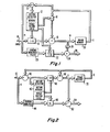
- FIGURES 1-3 are block diagrams of alternate embodiments of noise recursive filter systems embodying the present invention.
- FIGURE 4 is a block diagram of exemplary circuitry for generating scale factors for application to the scaling circuits in FIGURES 1-3.
- the noise reducing system of the invention is useful for processing video signals developed in accordance with conventional TV signal standards, with e.g. appropriate selection of memory size, the invention will be described as applied to the NTSC television standard. It is to be understood that the system may be implemented in either the analog or the digital domain, however, a digital implementation of the system will be described.
- interconnections constructed with broad arrows represent multiconductor connections for parallel-bit digital signals. Interconnections drawn with narrow arrows represent single conductor connections.
- digital video signal to be processed is applied to input port 10 and noise reduced signal is available at output port 28.
- the input video signal may be baseband composite video signal from an analog-to-digital converter (not shown) or it may be, for example, luminance signal with incompletely cancelled chrominance signal therein.
- the output signal is noise-reduced luminance signal with the chrominance component removed.
- the input video signal at input port 10 is coupled to a scaling circuit 14 which scales the input video signal by a factor (1-K).
- the scaled input signal is coupled to one input port of adder 18.
- the output port of adder 18 is coupled to the input port of a delay or memory device 30 which delays signal by substantially one frame period wherein a frame comprises two fields of NTSC video signal. Delayed signal from memory 30 is coupled to scaling circuit 16 which scales the delayed signal by a factor K.
- the scaled and delayed signal is applied to a second input port of adder 18.
- the delay period provided by memory 30 is selected so that the two signals applied to adder 18 are separated in time by precisely one frame period (or a multiple of frame periods).
- the signal S c is equal to the signal S B generated during the previous frame period.
- the current frame is designated frame n, and the current signal, S B , is written as SBn' then the signal S c is equal to the signal S B(n-1) .
- the signal S B(n-1) is given by the equation and the signals S B(n-i) may be expressed in similar fashion. Substituting the values of S C(n-i) into equation
- the chrominance component is 180 degrees out of phase from frame to frame. If values for the chrominance component C i are substituted for the sample values S i in equation (3) the polarity of the terms in the series alternate. For the chrominance component equation (3) reduces to
- Noise is considered differently since noise samples from frame to frame are not coherent regardless of the state of interframe image motion or non-motion.
- the assumption is made that the noise components of all of the samples have approximately equal RMS values.
- Noise power adds as the sum of the squares of the respective noise components and the RMS amplitude is the square root of the sum of the squares.
- the noise value N B is determined by substituting the noise component samples into equation (3) with each term squared. After simplifying, the result is
- the luminance signal to noise improvement at point B in the FIGURE 1 circuit approaches 4 (1+K)/(1-K) which is large for K approaching 1.
- the residual chrominance signal is removed from the noise-reduced luminance signal by combining a portion of the input chrominance component with the noise-reduced signal. This is accomplished in the FIGURE 1 circuit by applying the input signal at port 10 to the filter 20 which passes only those signal components in the band of frequencies normally occupied by chrominance signal.
- the chrominance signal from filter 20 is scaled in element 22 by the factor (K-1)/(1+K) and then combined with the noise reduced luminance in adder 24.
- the residual chrominance in the luminance signal has an amplitude of C in (1-K)/(1+K) from equation (8) while the chrominance signal from element 22 is C in (K-1)/(1 + K) which, when the two are additively combined, cancel leaving noise reduced luminance.
- delay element 26 coupling signal from adder 18 to adder 24 compensates for sample processing delays incurred in filter 20.
- FIGURE 1 recursive filtering is inactivated when interframe image motion is detected. This is accomplished by changing the value of K to zero which effectively disconnects the feedback from memory 30 and couples input signal from port 10 via adder 18 to adder 24 scaled by the factor "1" and via filter 20 to adder 24 scaled by the factor "-1".
- the chrominance component at point B is in phase with the chrominance component of the signal output of filter 20.
- the in-phase chrominance from filter 20 is subtracted from the chrominance component in the signal passed by adder 18 leaving only a luminance component and a noise component on output bus 28.
- the FIGURE 1 circuit operates as a band stop filter to eliminate the chrominance component from the input video signal during motion.
- Band-pass filter 20 is incorporated to provide low-pass filtered luminance during motion intervals. However, during non-motion intervals filter 20 is not necessary to the circuit. In these intervals, the input signal may be coupled directly to scaling circuit 22. In this instance the amplitude of the luminance component at output port 28 is reduced from the amplitude of the luminance component of the input signal. The amplitude of the luminance component at output 28 can be restored by appropriately amplifying the output signal.
- the signal-to-noise ratio of video signals is sufficiently acceptable so the viewer will readily tolerate a time interval for the system to converge to the desired signal-to-noise improvement. This is not so with regard to chrominance contamination of luminance signal.
- the elimination of chrominance should be realizable during the first frame of no image motion.
- the first frame of no image motion is defined herein as the frame period in which the image content of the current input frame is the same as the image content of the immediately preceding frame. This criterion is applied on a pixel basis. In other words, with regard to the overall image there may be areas of interframe image motion. However, each pixel, frame-to-frame, is processed independently of all other pixels.
- frame of no image motion thus applies to each pixel independently of the condition of motion or non motion of other pixels.
- the elimination of chrominance may be accomplished if the chrominance component at point B is forced to converge to a steady state value in the first frame of no motion.
- This condition is achieved with the use of three values of K for scaling circuits 14 and 16; the first value, K 1 , is used during image motion; the second value, K 21 is used during the first frame of no motion and the third value, K 3 , is used for all succeeding frames of no motion.
- K1 is equal to zero to inactivate the recursive filter part of the system and to lead incoming signal directly to the frame memory to insure that information is available to detect the cessation of motion.
- the value of K 3 is selected to provide the desired steady state signal-to-noise improvement.
- K 3 The selection of K 3 involves a trade-off between the extent of signal-to-noise achieveable, and the time required to achieve it and also the subjective difference between the signal-to-noise ratio of moving image objects versus that of non moving image objects.
- K 2 required to produce a steady state chrominance component at point B and consequently to permit elimination of chrominance in all frames of no motion is given by
- the scale factors are selected at the pixel rate or a small submultiple of the pixel rate.
- the values of K are dependent on interframe motion and the history of interframe motion.
- Differences between the luminance component of samples from successive frames are an indication that motion or no motion has occurred between frames. These differences are provided by subtractor 13 having its minuend and subtrahend inputs connected to the input port 10 and the output of memory 30. The differences are coupled to a motion detector-scale factor generator 12 which produces the respective scale factors for scaling circuits 14, 16 and 22. An illustrative motion detector scale factor generator will be described below with reference to FIGURE 4.
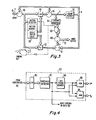
- FIGURE 2 is an alternative recursive filter noise reducing system.
- Input video samples, S A are applied at input port 10 and coupled to subtracter 40.
- Delayed samples S E from memory 30, are coupled to a second input port of subtracter 40 which produces the difference samples (SA-SE).
- SA-SE difference samples
- the respective samples S A and S E correspond to like pixels of successive image frames.
- the difference samples (S A -S E ) are applied to a scaling circuit 48 which produces scaled difference samples K m ( S A -S e ) where K m is a scale factor.
- the scaled difference samples and the delayed samples S E are applied to an adder 50 which produces sample sums S D given by the equation
- the scale factor K m is set to one and from equation (11) it is seen that the samples S D are equal to the input samples S A . After e.g. two frames of no motion the scale factor K m is set to a value K m3 . If no motion persists for a relatively large number of frame intervals it can be shown that the noise component S DN at the output of adder 50 converges to the value
- the scale factor K m is set to a value K m2 during the first frame of no motion.
- the value of K m2 is given by and the steady state chrominance component S DC is given by
- the luminance component S DY in the steady state, is equal to the luminance component at the input SAY.
- Input samples at port 10 are applied to a chrominance band-pass filter 44 which passes the chrominance component S AC , a luminance component S AYH which corresponds to the luminance signal in the chrominance band of frequencies, and a noise component to a scaling circuit 46 which scales the samples by a factor K 0 .
- the scaled samples K 0 (S AC +S AYH +S AN ) are coupled to adder 52.
- Samples S D consisting of components S DY , S DC and S DN from adder 50, are coupled to a second input port of adder 52 which develops the system output signal S 0 given by
- the chrominance component of samples S 0 are reduced to zero by setting the scale factor K 0 to the value -K m3 /(2-K m3 ).
- the lower frequency luminance component of samples So is equal to the luminance component samples S DY .
- the luminance component S OYH of samples S 0 in the chrominance frequency spectrum is equal to S AYH (2(1-K m3 )/(2-K m3 )). This is an undesirable reduction in high frequency luminance but, the amplitude may be restored by selectively peaking the output signal.
- the noise component S ON is developed from noise contributions passed through scaling circuit 46 and from the output of adder 50. Assuming the worst case i.e. that band-pass filter 44 passes all of the input noise component, the output noise component can be shown to be
- the ratio of the output noise component S ON to the noise component S DN is equal to 2(1-K m3 )/(2-K m3 ) which is less than 1 for all values of K m3 less than 1.
- the difference samples produced by subtracter 40 contain interframe motion information. These differences are applied to a motion detector-scale factor generator circuit 42 which develops the scale factors for scaling circuits 46 and 48 on e.g. a pixel-by-pixel basis i.e. a sample-by-sample basis. illustrativescale factors produced by circuit 42 are in Table I.
- the value K m3 will be some small value such as 1/8, 1/16 or 1/32.
- the FIGURE 2 system like the FIGURE 1 system reverts to a chrominance band stop or notch filter between the input and output ports during motion intervals.
- FIGURE 3 is a variation of the FIGURE 2 system. Elements of the FIGURE 3 circuit designated with like numbers to the FIGURE 2 circuit are similar devices.
- sample differences (S A- S E ) from subtracter 40 are applied to scaling circuit 62 which produces scaled sample differences K K (S A -S F ).
- the scaled sample differences are coupled to adder 70 wherein they are summed with samples S E from frame memory 30.
- the sums, S XT from adder 70, in the absence of motion, are coupled unchanged via subtracter 68 to the luminance output port 72 and are expressed by
- the luminance component of S A is equal to the luminance component of S E . From equation (16) it is seen therefore, that the output luminance component S XY is equal to the input luminance component SAY regardless of the value of K K .
- the higher frequency luminance component output by adder 70 are not attenuated as are the higher frequency luminance components output by the FIGURES 1 and 2 circuits.
- K K is set to one-half.
- the magnitude of the chrominance components of S A and S E will be equal but they will be anti-phase.
- the system performs as a luminance frame comb filter and the chrominance component output by adder 70 is zero.
- the chrominance component S xc will equal zero for K K equal to one-half for the first frame of no motion and K m3 /2 for all succeeding frames of no motion.
- the noise component S XN for the first frame of no motion is equal to the RMS value of the input noise divided by the square root of two.
- the chrominance component of signal S x is cancelled in subtracter 68 by the chrominance signal component S DC .
- the control for gating circuit 66 may be provided by the motion detector 60. In effect, the FIGURE 3 circuit reverts to a band stop filter for chrominance signal during image motion.
- Chrominance signal with a reduced luminance component may be developed by subtracting the luminance output signal S XY from appropriately delayed composite video signal from input 10. It is noted that during no motion periods the difference signals from subtracter 40 consists substantially of a chrominance signal whose amplitude is slightly larger than the amplitude of the input chrominance component.
- Table II lists the scale factors K m and K K as well as the gate control for the different conditions of interframe image motion for the FIGURE 3 system.
- the FIGURE 3 circuitry may be slightly rearranged to provide a further alternative embodiment.
- the signal input port of the scaling circuit 62 may be coupled to the output of scaling circuit 48 rather than the output of subtracter 40.
- the values of the scale factor K K must be appropriately changed so that the product of scale factors, K m K K , equal the respective values in Table II listed under the column headed K K .
- new values of K K are 1, (2-K m3 )/2 and 1/2 for no motion, the first frame post motion and steady state respectively.
- FIGURE 1-3 In designing the FIGURE 1-3 systems it may be necessary to interpose compensating delays in certain of the signal paths. Those skilled in the art of circuit design will readily recognize such requirements and be able to implement them.
- the systems have been described in terms of primarily producing a noise-reduced luminance signal from composite video signal or from a luminance input signal containing chrominance contamination. With slight alterations the system can be arranged to, for example, produce a noise reduced chrominance signal from composite video. This may be accomplished in the FIGURE 3 system by changing subtracter 40 to an adder and adders 50 and 70 to subtracters.
- the sequence of samples may be represented Y 1 -I 1 , Y 2 +Q 2 , Y 3 +I 3 , Y 4 -Q 4 , Y 5 -I 5' Y 6 +Q 6' Y 7 +I 7 , Y 8 -Q 8 ,...
- Corresponding samples on adjacent frame may be represented Y 1 +I 1 , Y 2 -Q 2 , Y 3 -I 3 , Y 4 + Q 4' Y 5 +I 5' Y 6 -Q 6 , Y 7 -I 7 , Y 8 +Q 8 ...
- the luminance and I, Q magnitudes of corresponding samples in the two sequences (frames) are equal (i.e. for no interframe motion)
- the samples from the first sequence are added to corresponding samples in the second sequence
- the luminance components, Y will combine constructively but the I, Q components will cancel.
- the system of FIGURE 3 operates on this principle to produce the luminance output signal.
- the first sequence may be considered to correspond to the samples S A and the second sequence to correspond to samples S E .
- the complemented sequence will have relative values represented by -(Y1+I1), -(Y 2 -Q 2 ), -(Y 3 -I 3 ), -(Y 4 +Q 4 ), -(Y 5 +I 5 ), -( Y 6 -Q 6 ) ' -(Y 7 -I 7 ), -(Y 8 +Q 8 )...which may be rewritten -I 1 -Y 1 , Q 2 -Y 2 , I 3 -Y 3 , -Q 4 -Y 4 , -I 5 -Y 5 , Q 6 -Y 6 , I 7 -Y 7 , -Q 8 -Y 8 ...
- the chrominance signal i.e. the I and Q color difference signals
- the chrominance signal has significantly less bandwidth than the luminance signal.
- a recursive filter arranged to produce the chrominance signal it is therefore not necessary to use all of the samples of the foregoing sequences and, thus, the size of the frame memory 30 can be reduced. For example two samples, one containing an - I component and one containing a Q component, from each set of four successive samples may be selected and processed. If this is done, however, provision must be made to select samples of opposite I, Q phase in alternate frames. For example, if the samples Y 1 -I 1 , Y 2 + Q 2 , Y 5 - I 5 , Y 6 + Q 6 etc. are selected from the first sequence then samples Y 1 +I 1 , Y 2 -Q 2 , Y 5 +I 5 , Y 6 -Q 6 etc. must be selected from the second sequence.
- FIGURE 4 shows an illustrative motion detector-scale factor generator.
- the circuitry shown is directed toward the FIGURE 3 system but with modifications that will be immediately apparent to those skilled in the art of circuit design can be made applicable to the FIGURE 1 and 2 systems.
- Sample differences from subtracter 40 are applied to a low-pass filter 80 to remove the chrominance component. This is necessary since chrominance has a 180 degree phase difference from frame-to-frame and, thus, combines constructively in subtracter 40 rather than providing the difference of the chrominance magnitudes.
- the low-pass filtered differences are applied to a threshold detector 82 which generates a logic one for the magnitude, i.e. the absolute value, of the differences being greater than a predetermined value and generates a logic zero for the magnitude of the differences being less than this value.
- the predetermined value or threshold is established to provide a degree of noise immunity in the detection of motion and will be determined by user or designer preference.
- Motion signal from detector 82 is coupled to the data input port of the memory device 84 which delays the motion signal by one frame period. Delayed motion signal from the memory device 84 and motion signal from the detector 82 are coupled to the address input ports of the ROM's 86 and 88 which are programmed to output the requisite scale factors for the motion states applied to their address input ports.
- Table III is an illustrative state table for the FIGURE 3 system.
- Table III is developed around a time sequence of frames running from top to bottom. The condition of interframe image motion was selected to provide all possible 2-bit address states to the ROM's 86 and 88.
- Note the value K m3 is selected arbitrarily in accordance with the desired system response time and degree of noise reduction.
- ROM's 86 and.88 will be programmed with the appropriate scale factors or scale factor control signals as described with reference to the FIGURES 1 and 2 systems.
Abstract
Description
- The present invention relates to reducing both noise and one of the chrominance or luminance components of a video signal.
- The use of recursive filters for reducing noise in video signals is relatively well known. Video recursive filters typically consist of a frame memory, two scaling circuits and an adder circuit. Incoming or current video signal is scaled by one of the scaling circuits and the scaled video signal is applied to one input port of the adder. Signal delayed by substantially one frame period from the output of the frame memory is scaled in the other of the scaling circuits and applied to a second input port of the adder. Video signal sums produced by the adder are coupled to the input of the frame memory and represent noise-reduced video.
- The foregoing description applies if the video signal is a monochrome or luminance signal. If the video signal is a chrominance component of composite video a signal chrominance phase inverter must be interposed between the adder circuit and the frame memory. Finally, if the video signal to be processed is composite video, and the desired system output signal is noise-reduced composite video signal, then circuitry must be inserted between the adder and frame memory to invert the phase of the chrominance component only, of the noise-reduced composite video signal. An example of this type of video recursive filter is disclosed in U.S. Patent No. 4,064,530 entitled "Noise Reduction System For Color Television".
- A recursive filter, which does not have provision for chrominance phase inversion, and to which composite video is applied tends to produce a noise reduced luminance component with a small amount of residual chrominance contamination after the occurrence of a number of frame periods in which there is no interframe image motion. Thus, a video recursive filter may be employed to partially separate the luminance component from composite video signal for non-moving images. Such a system has limited utility.
- One embodiment of the present invention providesluminance/chrominance separation from composite video signal without residual cross components using a recursive filter system.
- Another embodiment adaptively controls a luminance/chrominance separating recursive filter to rapidly reach steady state operation following cessation of interframe image motion.
- A further embodiment of the invention comprises a video signal recursive filter system which includes a delay or storage device for storing a noise-reduced video signal and a summing device for adding a portion of the stored signal to a portion of the current or incoming video signal to produce noise-reduced video signal. A signal combining circuit is arranged to subtract a further portion of current video signal from the noise-reduced video signal to produce a noise-reduced video signal having a predetermined component of the video signal substantially eliminated.
- The invention will now be described by way of example with reference to the accompanying drawings in which:
- FIGURES 1-3 are block diagrams of alternate embodiments of noise recursive filter systems embodying the present invention; and
- FIGURE 4 is a block diagram of exemplary circuitry for generating scale factors for application to the scaling circuits in FIGURES 1-3.
- Although the noise reducing system of the invention is useful for processing video signals developed in accordance with conventional TV signal standards, with e.g. appropriate selection of memory size, the invention will be described as applied to the NTSC television standard. It is to be understood that the system may be implemented in either the analog or the digital domain, however, a digital implementation of the system will be described. In the drawing, interconnections constructed with broad arrows represent multiconductor connections for parallel-bit digital signals. Interconnections drawn with narrow arrows represent single conductor connections.
- Referring to FIGURE 1, digital video signal to be processed is applied to
input port 10 and noise reduced signal is available atoutput port 28. The input video signal may be baseband composite video signal from an analog-to-digital converter (not shown) or it may be, for example, luminance signal with incompletely cancelled chrominance signal therein. For either input signal the output signal is noise-reduced luminance signal with the chrominance component removed. - The input video signal at
input port 10 is coupled to ascaling circuit 14 which scales the input video signal by a factor (1-K). The scaled input signal is coupled to one input port ofadder 18. The output port ofadder 18 is coupled to the input port of a delay ormemory device 30 which delays signal by substantially one frame period wherein a frame comprises two fields of NTSC video signal. Delayed signal frommemory 30 is coupled to scalingcircuit 16 which scales the delayed signal by a factor K. The scaled and delayed signal is applied to a second input port ofadder 18. The delay period provided bymemory 30 is selected so that the two signals applied toadder 18 are separated in time by precisely one frame period (or a multiple of frame periods). - If the signals at
input port 10, the output port ofadder 18 and the output port ofmemory 30 are designated SA, SB and Sc respectively, then the signal SB is given by
- The signal Sc is equal to the signal SB generated during the previous frame period. Thus, if the current frame is designated frame n, and the current signal, SB, is written as SBn' then the signal Sc is equal to the signal SB(n-1). The signal SB(n-1) is given by the equation

- (1) produces the result


- As n gets large, the series reduces to 1/(1-K) and equation (5) becomes

- The chrominance component is 180 degrees out of phase from frame to frame. If values for the chrominance component Ci are substituted for the sample values Si in equation (3) the polarity of the terms in the series alternate. For the chrominance component equation (3) reduces to

- In the limit as the number of K terms approach infinity the series with alternating signs tends towards the
value 1/(1+K). Substituting this value for the series in equation (7), in the limit becomes the chrominance component
- Noise is considered differently since noise samples from frame to frame are not coherent regardless of the state of interframe image motion or non-motion. The assumption is made that the noise components of all of the samples have approximately equal RMS values. Noise power adds as the sum of the squares of the respective noise components and the RMS amplitude is the square root of the sum of the squares. The noise value NB is determined by substituting the noise component samples into equation (3) with each term squared. After simplifying, the result is
-

value 1/(1-K2) so that equation (9) reduces to
- The luminance signal to noise improvement at point B in the FIGURE 1 circuit approaches 4 (1+K)/(1-K) which is large for K approaching 1.
- The residual chrominance signal is removed from the noise-reduced luminance signal by combining a portion of the input chrominance component with the noise-reduced signal. This is accomplished in the FIGURE 1 circuit by applying the input signal at
port 10 to thefilter 20 which passes only those signal components in the band of frequencies normally occupied by chrominance signal. The chrominance signal fromfilter 20 is scaled inelement 22 by the factor (K-1)/(1+K) and then combined with the noise reduced luminance inadder 24. - The residual chrominance in the luminance signal has an amplitude of Cin(1-K)/(1+K) from equation (8) while the chrominance signal from
element 22 is Cin(K-1)/(1+K) which, when the two are additively combined, cancel leaving noise reduced luminance. Note thatdelay element 26 coupling signal fromadder 18 to adder 24 compensates for sample processing delays incurred infilter 20. - The foregoing analysis assumed that there was no interframe image motion. When motion occurs it is generally accepted that a recursive filter produces undesirable results. In the FIGURE 1 system recursive filtering is inactivated when interframe image motion is detected. This is accomplished by changing the value of K to zero which effectively disconnects the feedback from
memory 30 and couples input signal fromport 10 viaadder 18 to adder 24 scaled by the factor "1" and viafilter 20 to adder 24 scaled by the factor "-1". The chrominance component at point B is in phase with the chrominance component of the signal output offilter 20. The in-phase chrominance fromfilter 20 is subtracted from the chrominance component in the signal passed byadder 18 leaving only a luminance component and a noise component onoutput bus 28. The FIGURE 1 circuit operates as a band stop filter to eliminate the chrominance component from the input video signal during motion. - Band-
pass filter 20 is incorporated to provide low-pass filtered luminance during motion intervals. However, during non-motion intervals filter 20 is not necessary to the circuit. In these intervals, the input signal may be coupled directly to scalingcircuit 22. In this instance the amplitude of the luminance component atoutput port 28 is reduced from the amplitude of the luminance component of the input signal. The amplitude of the luminance component atoutput 28 can be restored by appropriately amplifying the output signal. - Generally the signal-to-noise ratio of video signals is sufficiently acceptable so the viewer will readily tolerate a time interval for the system to converge to the desired signal-to-noise improvement. This is not so with regard to chrominance contamination of luminance signal. The elimination of chrominance should be realizable during the first frame of no image motion. The first frame of no image motion is defined herein as the frame period in which the image content of the current input frame is the same as the image content of the immediately preceding frame. This criterion is applied on a pixel basis. In other words, with regard to the overall image there may be areas of interframe image motion. However, each pixel, frame-to-frame, is processed independently of all other pixels. The term "frame of no image motion" thus applies to each pixel independently of the condition of motion or non motion of other pixels.
- .The elimination of chrominance may be accomplished if the chrominance component at point B is forced to converge to a steady state value in the first frame of no motion. This condition is achieved with the use of three values of K for scaling
circuits -

- Only two values are required for the scale factor K in the
scaling circuit 22 and these values are zero for motion periods and K3 for all non-motion periods. - The scale factors are selected at the pixel rate or a small submultiple of the pixel rate. The values of K are dependent on interframe motion and the history of interframe motion.
- Differences between the luminance component of samples from successive frames are an indication that motion or no motion has occurred between frames. These differences are provided by subtractor 13 having its minuend and subtrahend inputs connected to the
input port 10 and the output ofmemory 30. The differences are coupled to a motion detector-scale factor generator 12 which produces the respective scale factors for scalingcircuits - FIGURE 2 is an alternative recursive filter noise reducing system. Input video samples, SA, are applied at
input port 10 and coupled tosubtracter 40. Delayed samples SE, frommemory 30, are coupled to a second input port ofsubtracter 40 which produces the difference samples (SA-SE). The respective samples SA and SE correspond to like pixels of successive image frames. The difference samples (SA-SE) are applied to ascaling circuit 48 which produces scaled difference samples K m(S A-Se) where Km is a scale factor. The scaled difference samples and the delayed samples SE are applied to anadder 50 which produces sample sums SD given by the equation
- During periods of interframe image motion the scale factor Km is set to one and from equation (11) it is seen that the samples SD are equal to the input samples SA. After e.g. two frames of no motion the scale factor Km is set to a value Km3. If no motion persists for a relatively large number of frame intervals it can be shown that the noise component SDN at the output of
adder 50 converges to the value
- To insure that the chrominance component converges to a steady state value at the first frame of no motion, the scale factor Km is set to a value Km2 during the first frame of no motion. The value of Km2 is given by


- The luminance component SDY, in the steady state, is equal to the luminance component at the input SAY.
- Input samples at
port 10 are applied to a chrominance band-pass filter 44 which passes the chrominance component SAC, a luminance component SAYH which corresponds to the luminance signal in the chrominance band of frequencies, and a noise component to ascaling circuit 46 which scales the samples by a factor K0. The scaled samples K0(SAC+SAYH+SAN) are coupled to adder 52. Samples SD, consisting of components SDY, SDC and SDN fromadder 50, are coupled to a second input port ofadder 52 which develops the system output signal S0 given by
- The chrominance component of samples S0 are reduced to zero by setting the scale factor K0 to the value -Km3/(2-Km3).
- The lower frequency luminance component of samples So is equal to the luminance component samples SDY. The luminance component SOYH of samples S0, in the chrominance frequency spectrum is equal to SAYH(2(1-Km3)/(2-Km3)). This is an undesirable reduction in high frequency luminance but, the amplitude may be restored by selectively peaking the output signal.
- The noise component SON is developed from noise contributions passed through scaling
circuit 46 and from the output ofadder 50. Assuming the worst case i.e. that band-pass filter 44 passes all of the input noise component, the output noise component can be shown to be -

- The ratio of the output noise component SON to the noise component SDN is equal to 2(1-Km3)/(2-Km3) which is less than 1 for all values of Km3 less than 1.
- In the FIGURE 2 system the difference samples produced by
subtracter 40 contain interframe motion information. These differences are applied to a motion detector-scalefactor generator circuit 42 which develops the scale factors for scalingcircuits circuit 42 are in Table I.
- In Table I, the value Km3 will be some small value such as 1/8, 1/16 or 1/32.
- The FIGURE 2 system like the FIGURE 1 system reverts to a chrominance band stop or notch filter between the input and output ports during motion intervals.
- FIGURE 3 is a variation of the FIGURE 2 system. Elements of the FIGURE 3 circuit designated with like numbers to the FIGURE 2 circuit are similar devices.
- In FIGURE 3 sample differences (SA-SE) from
subtracter 40 are applied to scalingcircuit 62 which produces scaled sample differences KK(SA-SF). The scaled sample differences are coupled to adder 70 wherein they are summed with samples SE fromframe memory 30. The sums, SXT from adder 70, in the absence of motion, are coupled unchanged viasubtracter 68 to theluminance output port 72 and are expressed by -

- In the absence of motion, the luminance component of SA is equal to the luminance component of SE. From equation (16) it is seen therefore, that the output luminance component SXY is equal to the input luminance component SAY regardless of the value of KK. The higher frequency luminance component output by adder 70 are not attenuated as are the higher frequency luminance components output by the FIGURES 1 and 2 circuits.
- In the first frame of no motion KK is set to one-half. The magnitude of the chrominance components of SA and SE will be equal but they will be anti-phase. Thus, during this frame interval the system performs as a luminance frame comb filter and the chrominance component output by adder 70 is zero.
- If the value of Km for the first frame of no motion is selected to cause the chrominance component of SD to converge immediately, then with respect to the chrominance component SXC in the second frame of no motion, equation (18) becomes
-

- The chrominance component Sxc will equal zero for KK equal to one-half for the first frame of no motion and Km3/2 for all succeeding frames of no motion.
- The RMS value of the noise component SXN converges toward the RMS input noise value times the square root of (Km3/2), which is smaller than the value of the noise component of the samples SD for small Km3 and approaches the
value 1 2 times the noise component of sample SD forK m3 =1. The noise component SXN for the first frame of no motion is equal to the RMS value of the input noise divided by the square root of two. - The value of the scale factor KK is set to "1" during interframe image motion. From equation (17) it is seen that the output signal Sx is equal to the input signal SA. Similarly from equation (11) the signal SD is equal to SA (for Km=1). The signal SD is applied to a band-
pass filter 64 which extracts the chrominance component. The chrominance component SDC=SAC is coupled during interframe image motion periods to the subtrahend input ofsubtracter 68 by thegating circuit 66. The chrominance component of signal Sx is cancelled insubtracter 68 by the chrominance signal component SDC. The control for gatingcircuit 66 may be provided by themotion detector 60. In effect, the FIGURE 3 circuit reverts to a band stop filter for chrominance signal during image motion. - Chrominance signal with a reduced luminance component may be developed by subtracting the luminance output signal SXY from appropriately delayed composite video signal from
input 10. It is noted that during no motion periods the difference signals fromsubtracter 40 consists substantially of a chrominance signal whose amplitude is slightly larger than the amplitude of the input chrominance component. - Table II lists the scale factors Km and KK as well as the gate control for the different conditions of interframe image motion for the FIGURE 3 system.

- The FIGURE 3 circuitry may be slightly rearranged to provide a further alternative embodiment. In such alternate embodiment the signal input port of the scaling
circuit 62 may be coupled to the output of scalingcircuit 48 rather than the output ofsubtracter 40. The values of the scale factor KK must be appropriately changed so that the product of scale factors, Km KK, equal the respective values in Table II listed under the column headed KK. For example, new values of KK are 1, (2-Km3)/2 and 1/2 for no motion, the first frame post motion and steady state respectively. - In designing the FIGURE 1-3 systems it may be necessary to interpose compensating delays in certain of the signal paths. Those skilled in the art of circuit design will readily recognize such requirements and be able to implement them.
- The systems have been described in terms of primarily producing a noise-reduced luminance signal from composite video signal or from a luminance input signal containing chrominance contamination. With slight alterations the system can be arranged to, for example, produce a noise reduced chrominance signal from composite video. This may be accomplished in the FIGURE 3 system by changing
subtracter 40 to an adder andadders 50 and 70 to subtracters. - This may be understood by assuming that the composite video signal is sampled synchronous to the color burst reference and at four times the color subcarrier frequency. If the sampling phase is selected to coincide with the I and Q color difference sginal axes the sequence of samples may be represented Y1-I1, Y2+Q2, Y3+I3, Y4-Q4, Y5-I5' Y6+Q6' Y7+I7, Y8-Q8,... Corresponding samples on adjacent frame, because chrominance is inverted, may be represented Y1+I1, Y2-Q2, Y3-I3, Y 4 +Q4' Y 5 +I 5' Y6-Q6, Y7-I7, Y8+Q8... If the luminance and I, Q magnitudes of corresponding samples in the two sequences (frames) are equal (i.e. for no interframe motion), and the samples from the first sequence are added to corresponding samples in the second sequence, the luminance components, Y, will combine constructively but the I, Q components will cancel. The system of FIGURE 3 operates on this principle to produce the luminance output signal. In FIGURE 3, the first sequence may be considered to correspond to the samples SA and the second sequence to correspond to samples S E.
- Now consider complementing (inverting) the samples in the second sequence. The complemented sequence will have relative values represented by -(Y1+I1), -(Y2-Q2), -(Y3-I3), -(Y4+Q4), -(Y5+I5), -(Y 6-Q6)' -(Y7-I7), -(Y8+Q8)...which may be rewritten -I1-Y1, Q2-Y2, I3-Y3, -Q4-Y4, -I5-Y5, Q6-Y6, I7-Y7, -Q8-Y8... Comparing this latter sequence with the first sequence it will be seen that corresponding I, Q component samples are all in phase i.e. have like polarities while the luminance component samples have opposite polarity. Thus, if the complemented version is applied as signal SE in the FIGURE 3 system, the I, Q components will combine constructively and the luminance component will cancel. The effect of complementing the signal SE, i.e. the output of
frame memory 30 may be realized by complementing the inputs tosubtracter 40 andadders 50 and 70 to which the samples SE are coupled. But this is the same as changingsubtracter 40 to an adder, andadders 50 and 70 to subtracters with the samples SE coupled as subtrahends to the subtracters. - The chrominance signal i.e. the I and Q color difference signals, has significantly less bandwidth than the luminance signal. In a recursive filter arranged to produce the chrominance signal it is therefore not necessary to use all of the samples of the foregoing sequences and, thus, the size of the
frame memory 30 can be reduced. For example two samples, one containing an-I component and one containing a Q component, from each set of four successive samples may be selected and processed. If this is done, however, provision must be made to select samples of opposite I, Q phase in alternate frames. For example, if the samples Y1-I1, Y2 +Q2, Y5-I 5, Y 6 +Q6 etc. are selected from the first sequence then samples Y1+I1, Y2-Q2, Y5+I5, Y6-Q6 etc. must be selected from the second sequence. - Similar modifications can be made to the FIGURE 1 and 2 systems.
- FIGURE 4 shows an illustrative motion detector-scale factor generator. The circuitry shown is directed toward the FIGURE 3 system but with modifications that will be immediately apparent to those skilled in the art of circuit design can be made applicable to the FIGURE 1 and 2 systems.
- Sample differences from
subtracter 40 are applied to a low-pass filter 80 to remove the chrominance component. This is necessary since chrominance has a 180 degree phase difference from frame-to-frame and, thus, combines constructively insubtracter 40 rather than providing the difference of the chrominance magnitudes. The low-pass filtered differences are applied to athreshold detector 82 which generates a logic one for the magnitude, i.e. the absolute value, of the differences being greater than a predetermined value and generates a logic zero for the magnitude of the differences being less than this value. The predetermined value or threshold is established to provide a degree of noise immunity in the detection of motion and will be determined by user or designer preference. - Motion signal from
detector 82 is coupled to the data input port of thememory device 84 which delays the motion signal by one frame period. Delayed motion signal from thememory device 84 and motion signal from thedetector 82 are coupled to the address input ports of the ROM's 86 and 88 which are programmed to output the requisite scale factors for the motion states applied to their address input ports. Table III is an illustrative state table for the FIGURE 3 system.
- Table III is developed around a time sequence of frames running from top to bottom. The condition of interframe image motion was selected to provide all possible 2-bit address states to the ROM's 86 and 88. The columns labeled "
Detector 82 Output" and "Memory 84 Output" taken together form the address codes for the ROM's 86 and,88. Note the value Km3 is selected arbitrarily in accordance with the desired system response time and degree of noise reduction. - For adaptation to the FIGURES 1 and 2 noise-reducing systems, ROM's 86 and.88 will be programmed with the appropriate scale factors or scale factor control signals as described with reference to the FIGURES 1 and 2 systems.
Claims (14)
Priority Applications (1)
| Application Number | Priority Date | Filing Date | Title |
|---|---|---|---|
| AT86302024T ATE53730T1 (en) | 1985-03-25 | 1986-03-19 | RECURSIVE FILTER FOR VIDEO SIGNALS WITH SEPARATION OF LUMINANCE AND COLOR INFORMATION. |
Applications Claiming Priority (2)
| Application Number | Priority Date | Filing Date | Title |
|---|---|---|---|
| US715811 | 1985-03-25 | ||
| US06/715,811 US4646138A (en) | 1985-03-25 | 1985-03-25 | Video signal recursive filter with luma/chroma separation |
Publications (2)
| Publication Number | Publication Date |
|---|---|
| EP0196193A1 true EP0196193A1 (en) | 1986-10-01 |
| EP0196193B1 EP0196193B1 (en) | 1990-06-13 |
Family
ID=24875582
Family Applications (1)
| Application Number | Title | Priority Date | Filing Date |
|---|---|---|---|
| EP86302024A Expired - Lifetime EP0196193B1 (en) | 1985-03-25 | 1986-03-19 | A video signal recursive filter with luma/chroma separation |
Country Status (10)
| Country | Link |
|---|---|
| US (1) | US4646138A (en) |
| EP (1) | EP0196193B1 (en) |
| JP (1) | JPH0748862B2 (en) |
| KR (1) | KR940002161B1 (en) |
| AT (1) | ATE53730T1 (en) |
| AU (1) | AU589610B2 (en) |
| CA (1) | CA1233240A (en) |
| DE (1) | DE3672066D1 (en) |
| ES (1) | ES8707642A1 (en) |
| SG (1) | SG29593G (en) |
Cited By (4)
| Publication number | Priority date | Publication date | Assignee | Title |
|---|---|---|---|---|
| GB2228161A (en) * | 1989-01-10 | 1990-08-15 | Broadcast Television Syst | Adaptive colour decoder |
| EP0423320A1 (en) * | 1989-04-28 | 1991-04-24 | SPEARS, Steven | Video noise reduction system |
| DE4116762A1 (en) * | 1991-05-23 | 1992-11-26 | Roland Man Druckmasch | DEVICE FOR WASHING A CYLINDER OF A PRINTING MACHINE |
| EP0601655A1 (en) * | 1992-12-10 | 1994-06-15 | Koninklijke Philips Electronics N.V. | Noise reduction filter |
Families Citing this family (26)
| Publication number | Priority date | Publication date | Assignee | Title |
|---|---|---|---|---|
| US4752826A (en) * | 1986-10-20 | 1988-06-21 | The Grass Valley Group, Inc. | Intra-field recursive interpolator |
| JPH07101924B2 (en) * | 1987-10-26 | 1995-11-01 | パイオニア株式会社 | Video signal noise eliminator |
| JPH01204573A (en) * | 1988-02-10 | 1989-08-17 | Sony Corp | Noise reduction circuit |
| US5790177A (en) * | 1988-10-17 | 1998-08-04 | Kassatly; Samuel Anthony | Digital signal recording/reproduction apparatus and method |
| GB8826463D0 (en) * | 1988-11-11 | 1988-12-14 | Rca Licensing Corp | Technique for actv side-panel noise reduction |
| US4890162A (en) * | 1989-01-26 | 1989-12-26 | Rca Licensing Corporation | Adjustable antialias filters |
| JPH0411466A (en) * | 1990-04-28 | 1992-01-16 | Sony Corp | Noise reducer |
| US5173776A (en) * | 1990-06-06 | 1992-12-22 | Electroscan Corporation | Apparatus and method for improving the signal-to-noise ratio of video display signals |
| FR2667475B1 (en) * | 1990-09-28 | 1992-10-30 | Thomson Consumer Electronics | METHOD FOR MEASURING NOISE IN AN ACTIVE VIDEO IMAGE AND DEVICE FOR CARRYING OUT THE METHOD. |
| US5278638A (en) * | 1991-09-30 | 1994-01-11 | Pioneer Electronic Corporation | Noise reducing circuit for images |
| US5309237A (en) * | 1992-03-31 | 1994-05-03 | Siemens Corporate Research, Inc. | Apparatus and method of compensating image-sequences for motion |
| JPH07162718A (en) * | 1993-12-10 | 1995-06-23 | Nikon Corp | Cyclic noise reducing device |
| US5438374A (en) * | 1993-12-10 | 1995-08-01 | At&T Corp. | System and method for filtering video signals |
| EP0705043B1 (en) * | 1994-09-30 | 2001-03-07 | STMicroelectronics S.r.l. | Device and method for filtering video images |
| KR100202565B1 (en) * | 1996-03-23 | 1999-06-15 | 구자홍 | The stereoscopic brightness/chrominance separating apparatus of composite image signal |
| KR100200702B1 (en) * | 1996-06-05 | 1999-06-15 | 윤종용 | Digital video encoder in digital video system |
| US7420625B1 (en) * | 2003-05-20 | 2008-09-02 | Pixelworks, Inc. | Fuzzy logic based adaptive Y/C separation system and method |
| US20060139494A1 (en) * | 2004-12-29 | 2006-06-29 | Samsung Electronics Co., Ltd. | Method of temporal noise reduction in video sequences |
| KR20070012047A (en) * | 2005-07-22 | 2007-01-25 | 삼성전자주식회사 | Digital video processing apparatus and control method thereof |
| US8090210B2 (en) * | 2006-03-30 | 2012-01-03 | Samsung Electronics Co., Ltd. | Recursive 3D super precision method for smoothly changing area |
| GB2438659B (en) * | 2006-06-02 | 2011-03-23 | Tandberg Television Asa | Recursive filtering of a video image using activity mapping |
| JP4589276B2 (en) * | 2006-08-07 | 2010-12-01 | トヨタ自動車株式会社 | Variable intake system for V-type internal combustion engine |
| TWI392334B (en) * | 2009-04-22 | 2013-04-01 | Mstar Semiconductor Inc | Image processing apparatus and image processing method |
| US8760466B1 (en) * | 2010-01-18 | 2014-06-24 | Pixar | Coherent noise for non-photorealistic rendering |
| US8675137B2 (en) * | 2010-04-13 | 2014-03-18 | Newport Media, Inc. | Apparatus and method for adaptive filtering |
| JP5937548B2 (en) * | 2013-06-26 | 2016-06-22 | 古野電気株式会社 | Digital filter and signal processing apparatus |
Citations (2)
| Publication number | Priority date | Publication date | Assignee | Title |
|---|---|---|---|---|
| US4064530A (en) * | 1976-11-10 | 1977-12-20 | Cbs Inc. | Noise reduction system for color television |
| GB2102651A (en) * | 1978-03-08 | 1983-02-02 | Tokyo Broadcasting Syst | Noise reduction system for color television signal |
Family Cites Families (18)
| Publication number | Priority date | Publication date | Assignee | Title |
|---|---|---|---|---|
| GB1469101A (en) * | 1973-03-23 | 1977-03-30 | Dolby Laboratories Inc | Noise reduction systems |
| US4240106A (en) * | 1976-10-14 | 1980-12-16 | Micro Consultants, Limited | Video noise reduction |
| US4573070A (en) * | 1977-01-31 | 1986-02-25 | Cooper J Carl | Noise reduction system for video signals |
| US4305091B2 (en) * | 1977-01-31 | 1998-02-10 | J Carl Cooper | Electronics noise reducing apparatus and method |
| FR2387557A1 (en) * | 1977-04-14 | 1978-11-10 | Telediffusion Fse | NOISE VISIBILITY REDUCTION SYSTEMS ON TELEVISION IMAGES |
| JPS5510228A (en) * | 1978-07-05 | 1980-01-24 | Nec Corp | S/n improving unit for television video signal |
| JPS592227B2 (en) * | 1978-08-21 | 1984-01-17 | 株式会社日立製作所 | Noise removal method |
| US4275418A (en) * | 1978-09-14 | 1981-06-23 | Micro Consultants Limited | Video noise reduction systems |
| GB2031686B (en) * | 1978-09-14 | 1983-02-02 | Micro Consultants Ltd | Movement detection |
| US4291333A (en) * | 1979-05-22 | 1981-09-22 | Fernseh Inc. | Noise filter |
| US4392123A (en) * | 1980-06-02 | 1983-07-05 | The Dindima Group Pty. Ltd. | Signal-to-noise improving system |
| US4390894A (en) * | 1980-08-20 | 1983-06-28 | U.S. Philips Corporation | Noise suppression circuit for a video signal |
| US4500911A (en) * | 1981-05-25 | 1985-02-19 | Nippon Hoso Kyokai | Noise reduction apparatus |
| DE3121597C3 (en) * | 1981-05-30 | 1993-09-30 | Bosch Gmbh Robert | System for reducing noise in a television picture signal |
| DE3150008A1 (en) * | 1981-12-17 | 1983-08-25 | Robert Bosch Gmbh, 7000 Stuttgart | System for reducing noise in a television signal |
| US4472733A (en) * | 1982-09-01 | 1984-09-18 | Rca Corporation | Color channel signal-to-noise improvement in digital television |
| US4538178A (en) * | 1983-06-24 | 1985-08-27 | Rca Corporation | Digital signal peaking apparatus with controllable peaking level |
| AU3034384A (en) * | 1983-07-08 | 1985-01-10 | N.V. Philips Gloeilampenfabrieken | Video nose reduction |
-
1985
- 1985-03-25 US US06/715,811 patent/US4646138A/en not_active Expired - Fee Related
-
1986
- 1986-03-18 ES ES553110A patent/ES8707642A1/en not_active Expired
- 1986-03-18 CA CA000504412A patent/CA1233240A/en not_active Expired
- 1986-03-18 AU AU54812/86A patent/AU589610B2/en not_active Ceased
- 1986-03-19 DE DE8686302024T patent/DE3672066D1/en not_active Expired - Fee Related
- 1986-03-19 AT AT86302024T patent/ATE53730T1/en not_active IP Right Cessation
- 1986-03-19 EP EP86302024A patent/EP0196193B1/en not_active Expired - Lifetime
- 1986-03-24 JP JP61067032A patent/JPH0748862B2/en not_active Expired - Lifetime
- 1986-03-25 KR KR1019860002209A patent/KR940002161B1/en not_active IP Right Cessation
-
1993
- 1993-03-18 SG SG295/93A patent/SG29593G/en unknown
Patent Citations (2)
| Publication number | Priority date | Publication date | Assignee | Title |
|---|---|---|---|---|
| US4064530A (en) * | 1976-11-10 | 1977-12-20 | Cbs Inc. | Noise reduction system for color television |
| GB2102651A (en) * | 1978-03-08 | 1983-02-02 | Tokyo Broadcasting Syst | Noise reduction system for color television signal |
Cited By (5)
| Publication number | Priority date | Publication date | Assignee | Title |
|---|---|---|---|---|
| GB2228161A (en) * | 1989-01-10 | 1990-08-15 | Broadcast Television Syst | Adaptive colour decoder |
| EP0423320A1 (en) * | 1989-04-28 | 1991-04-24 | SPEARS, Steven | Video noise reduction system |
| EP0423320A4 (en) * | 1989-04-28 | 1992-10-28 | Steven Spears | Video noise reduction system |
| DE4116762A1 (en) * | 1991-05-23 | 1992-11-26 | Roland Man Druckmasch | DEVICE FOR WASHING A CYLINDER OF A PRINTING MACHINE |
| EP0601655A1 (en) * | 1992-12-10 | 1994-06-15 | Koninklijke Philips Electronics N.V. | Noise reduction filter |
Also Published As
| Publication number | Publication date |
|---|---|
| US4646138A (en) | 1987-02-24 |
| ES553110A0 (en) | 1987-08-01 |
| AU5481286A (en) | 1986-10-02 |
| CA1233240A (en) | 1988-02-23 |
| KR860007828A (en) | 1986-10-17 |
| JPH0748862B2 (en) | 1995-05-24 |
| DE3672066D1 (en) | 1990-07-19 |
| AU589610B2 (en) | 1989-10-19 |
| EP0196193B1 (en) | 1990-06-13 |
| ATE53730T1 (en) | 1990-06-15 |
| SG29593G (en) | 1993-05-21 |
| ES8707642A1 (en) | 1987-08-01 |
| KR940002161B1 (en) | 1994-03-18 |
| JPS61224609A (en) | 1986-10-06 |
Similar Documents
| Publication | Publication Date | Title |
|---|---|---|
| EP0196193B1 (en) | A video signal recursive filter with luma/chroma separation | |
| KR100388579B1 (en) | Luma/chroma separation filter with common delay element | |
| GB2173066A (en) | Adaptive control of a recursive filter | |
| KR940003052B1 (en) | Video signal noise reduction apparatus | |
| MXPA97008123A (en) | Luma / chrome separation filter with derressive element co | |
| JPH04126489A (en) | Brightness/chromaticity separating circuit of composite picture signal | |
| EP0549174B1 (en) | Adaptive chrominance filtering control | |
| US5386249A (en) | Video motion detector with full-band response except for diagonal spatial frequencies | |
| KR100320901B1 (en) | Motion detection circuit | |
| US4636840A (en) | Adaptive luminance-chrominance separation apparatus | |
| GB2206466A (en) | Adaptive y/c separation apparatus for tv signals | |
| US5640211A (en) | Luminance signal/color signal separator circuit | |
| JPH0348715B2 (en) | ||
| US4636842A (en) | Comb filter "hanging dot" eliminator | |
| EP0125724B1 (en) | Movement-adaptive transversal-recursive noise suppression circuit for a television signal | |
| US6333764B1 (en) | Video signal luminance and chrominance separation | |
| KR930008183B1 (en) | Y/c separate system | |
| EP0648385B1 (en) | Signal processing | |
| KR940004558B1 (en) | Luma/chroma separation for tv receiver | |
| JPH0338991A (en) | Luminance signal/chrominance signal separating circuit | |
| KR950004652Y1 (en) | Luma/chroma separation apparatus | |
| KR960014243B1 (en) | Circuit of separating ntsc composite video signal component | |
| JPH0380787A (en) | Adaptive notch filter | |
| JPS6333990A (en) | Television signal processing system | |
| JPH0313194A (en) | Notched filter |
Legal Events
| Date | Code | Title | Description |
|---|---|---|---|
| PUAI | Public reference made under article 153(3) epc to a published international application that has entered the european phase |
Free format text: ORIGINAL CODE: 0009012 |
|
| AK | Designated contracting states |
Kind code of ref document: A1 Designated state(s): AT DE FR GB IT |
|
| 17P | Request for examination filed |
Effective date: 19870310 |
|
| RAP1 | Party data changed (applicant data changed or rights of an application transferred) |
Owner name: RCA LICENSING CORPORATION |
|
| 17Q | First examination report despatched |
Effective date: 19890621 |
|
| GRAA | (expected) grant |
Free format text: ORIGINAL CODE: 0009210 |
|
| AK | Designated contracting states |
Kind code of ref document: B1 Designated state(s): AT DE FR GB IT |
|
| REF | Corresponds to: |
Ref document number: 53730 Country of ref document: AT Date of ref document: 19900615 Kind code of ref document: T |
|
| ITF | It: translation for a ep patent filed |
Owner name: ING. C. GREGORJ S.P.A. |
|
| REF | Corresponds to: |
Ref document number: 3672066 Country of ref document: DE Date of ref document: 19900719 |
|
| ET | Fr: translation filed | ||
| ITTA | It: last paid annual fee | ||
| PLBE | No opposition filed within time limit |
Free format text: ORIGINAL CODE: 0009261 |
|
| STAA | Information on the status of an ep patent application or granted ep patent |
Free format text: STATUS: NO OPPOSITION FILED WITHIN TIME LIMIT |
|
| 26N | No opposition filed | ||
| PGFP | Annual fee paid to national office [announced via postgrant information from national office to epo] |
Ref country code: DE Payment date: 19940207 Year of fee payment: 9 |
|
| PGFP | Annual fee paid to national office [announced via postgrant information from national office to epo] |
Ref country code: AT Payment date: 19940208 Year of fee payment: 9 |
|
| PGFP | Annual fee paid to national office [announced via postgrant information from national office to epo] |
Ref country code: FR Payment date: 19940211 Year of fee payment: 9 |
|
| PGFP | Annual fee paid to national office [announced via postgrant information from national office to epo] |
Ref country code: GB Payment date: 19940301 Year of fee payment: 9 |
|
| PG25 | Lapsed in a contracting state [announced via postgrant information from national office to epo] |
Ref country code: GB Effective date: 19950319 Ref country code: AT Effective date: 19950319 |
|
| GBPC | Gb: european patent ceased through non-payment of renewal fee |
Effective date: 19950319 |
|
| PG25 | Lapsed in a contracting state [announced via postgrant information from national office to epo] |
Ref country code: FR Free format text: LAPSE BECAUSE OF NON-PAYMENT OF DUE FEES Effective date: 19951130 |
|
| PG25 | Lapsed in a contracting state [announced via postgrant information from national office to epo] |
Ref country code: DE Effective date: 19951201 |
|
| REG | Reference to a national code |
Ref country code: FR Ref legal event code: ST |
|
| PG25 | Lapsed in a contracting state [announced via postgrant information from national office to epo] |
Ref country code: IT Free format text: LAPSE BECAUSE OF NON-PAYMENT OF DUE FEES;WARNING: LAPSES OF ITALIAN PATENTS WITH EFFECTIVE DATE BEFORE 2007 MAY HAVE OCCURRED AT ANY TIME BEFORE 2007. THE CORRECT EFFECTIVE DATE MAY BE DIFFERENT FROM THE ONE RECORDED. Effective date: 20050319 |