EP0195935A2 - Process for manufacturing a circuit board comprising rigid and flexible parts for printed circuits - Google Patents
Process for manufacturing a circuit board comprising rigid and flexible parts for printed circuits Download PDFInfo
- Publication number
- EP0195935A2 EP0195935A2 EP86102244A EP86102244A EP0195935A2 EP 0195935 A2 EP0195935 A2 EP 0195935A2 EP 86102244 A EP86102244 A EP 86102244A EP 86102244 A EP86102244 A EP 86102244A EP 0195935 A2 EP0195935 A2 EP 0195935A2
- Authority
- EP
- European Patent Office
- Prior art keywords
- rigid
- circuit board
- flexible
- insulating material
- plate
- Prior art date
- Legal status (The legal status is an assumption and is not a legal conclusion. Google has not performed a legal analysis and makes no representation as to the accuracy of the status listed.)
- Withdrawn
Links
Images

Classifications
-
- H—ELECTRICITY
- H05—ELECTRIC TECHNIQUES NOT OTHERWISE PROVIDED FOR
- H05K—PRINTED CIRCUITS; CASINGS OR CONSTRUCTIONAL DETAILS OF ELECTRIC APPARATUS; MANUFACTURE OF ASSEMBLAGES OF ELECTRICAL COMPONENTS
- H05K1/00—Printed circuits
- H05K1/02—Details
- H05K1/0213—Electrical arrangements not otherwise provided for
- H05K1/0216—Reduction of cross-talk, noise or electromagnetic interference
-
- H—ELECTRICITY
- H05—ELECTRIC TECHNIQUES NOT OTHERWISE PROVIDED FOR
- H05K—PRINTED CIRCUITS; CASINGS OR CONSTRUCTIONAL DETAILS OF ELECTRIC APPARATUS; MANUFACTURE OF ASSEMBLAGES OF ELECTRICAL COMPONENTS
- H05K3/00—Apparatus or processes for manufacturing printed circuits
- H05K3/46—Manufacturing multilayer circuits
- H05K3/4688—Composite multilayer circuits, i.e. comprising insulating layers having different properties
- H05K3/4691—Rigid-flexible multilayer circuits comprising rigid and flexible layers, e.g. having in the bending regions only flexible layers
-
- H—ELECTRICITY
- H05—ELECTRIC TECHNIQUES NOT OTHERWISE PROVIDED FOR
- H05K—PRINTED CIRCUITS; CASINGS OR CONSTRUCTIONAL DETAILS OF ELECTRIC APPARATUS; MANUFACTURE OF ASSEMBLAGES OF ELECTRICAL COMPONENTS
- H05K1/00—Printed circuits
- H05K1/02—Details
- H05K1/03—Use of materials for the substrate
- H05K1/0313—Organic insulating material
- H05K1/0353—Organic insulating material consisting of two or more materials, e.g. two or more polymers, polymer + filler, + reinforcement
- H05K1/036—Multilayers with layers of different types
-
- H—ELECTRICITY
- H05—ELECTRIC TECHNIQUES NOT OTHERWISE PROVIDED FOR
- H05K—PRINTED CIRCUITS; CASINGS OR CONSTRUCTIONAL DETAILS OF ELECTRIC APPARATUS; MANUFACTURE OF ASSEMBLAGES OF ELECTRICAL COMPONENTS
- H05K2201/00—Indexing scheme relating to printed circuits covered by H05K1/00
- H05K2201/03—Conductive materials
- H05K2201/0332—Structure of the conductor
- H05K2201/0335—Layered conductors or foils
- H05K2201/0355—Metal foils
-
- H—ELECTRICITY
- H05—ELECTRIC TECHNIQUES NOT OTHERWISE PROVIDED FOR
- H05K—PRINTED CIRCUITS; CASINGS OR CONSTRUCTIONAL DETAILS OF ELECTRIC APPARATUS; MANUFACTURE OF ASSEMBLAGES OF ELECTRICAL COMPONENTS
- H05K2201/00—Indexing scheme relating to printed circuits covered by H05K1/00
- H05K2201/09—Shape and layout
- H05K2201/09009—Substrate related
- H05K2201/0909—Preformed cutting or breaking line
Definitions
- the present invention relates to a method for producing a rigid and flexible circuit board for printed electrical circuits, in which at least one rigid and at least one flexible insulating material layer are sandwiched together, the rigid insulating material layer only covers parts of the flexible insulating material layer and at least the flexible insulating material layer electrically Carries conductor tracks.
- Printed circuit boards of the type mentioned as well as various methods for producing the same are known.
- Several of the known production methods each start from a plate which forms the future rigid insulating material layer and which has larger dimensions than the printed circuit board to be produced.
- This plate will be provided with continuous slots at the future transition points between a rigid and a flexible part of the circuit board, the ends of which lie within the contours of the plate, but outside the future contours of the circuit board to be produced.
- a flexible film forming the future flexible insulating material layer is arranged on one side of the board, running over the slots thereof, and connected to the board by means of an adhesive film placed therebetween using pressure and heat.
- the flexible film carries electrical conductor tracks or on its side facing away from the plate a copper layer from which electrical conductor tracks can be formed.
- the conductor tracks and associated bores in the printed circuit board are then finished in the customary manner, after which the plate and the flexible film connected to it are severed along the contour lines of the printed circuit board, the contour lines crossing the end parts of the slots in the plate.
- the area bounded by the slots and the K o ntur baine and future Parts of the board covering flexible parts of the printed circuit board are finally detached from the flexible film and removed.
- a rigid board is generally used, which is laminated on its side to be turned away from the flexible film with a copper layer, which allows the formation of conductor tracks.
- a flexible insulating material film is used, which is laminated on its side to be turned away from the rigid plate with a copper layer to form conductor tracks.
- the desired conductor tracks can be produced in a known manner from the aforementioned copper layers in a photo-chemical way, and conductor holes on one and on the other side of the circuit board can be electrically connected to one another by means of associated bores and galvanic plating.
- the slits created in the rigid plate may have a disruptive effect because these slits are open on the side of the rigid plate facing away from the flexible film and allow the entry of chemicals and other foreign substances. This is particularly disadvantageous or even unacceptable if the side of the flexible film facing the rigid plate already carries conductor tracks which extend beyond the slots and may no longer be etched away.
- the slots in the rigid plate are not formed continuously but in the form of grooves which are only open on the side of the plate on which the flexible insulating material film is attached.
- the flexible film prevents the entry of foreign matter into the grooves.
- additional grooves have to be milled in this method on the side of the plate facing away from the flexible film, which grooves together form continuous slots with the first-mentioned grooves in order to enable the removal of the parts of the rigid plate covering the future flexible parts of the printed circuit board. If the first and the second grooves do not match exactly, undesirable shoulders or steps result on the flanks of the continuous slots. To avoid this, a relatively high precision in the positioning of the first and second grooves is required.
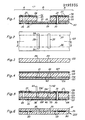
- the circuit board 20 shown schematically in FIG. 1 has rigid parts A and flexible parts B, the latter of which only a single one can be seen in FIG. 1.
- the printed circuit board 20 is composed of a plurality of layers arranged one above the other and connected to one another, as follows: A flexible insulating material layer 21 is connected by means of an adhesive layer 22 to a rigid insulating material layer 23, which only partially, namely on the rigid parts A, the flexible insulating material layer 21 the printed circuit board covered.
- the side of the flexible insulating material layer 21 facing away from the rigid insulating material layer 23 carries electrical conductor tracks 24 and a covering layer 25 made of insulating material and covers the latter.
- the printed circuit board 20 is also provided with through bores 29 and 30 which are assigned to the conductor tracks 27 and 24 and 27, respectively.
- individual conductor tracks 24 of the flexible layer 21 and individual conductor tracks 27 of the rigid layer 23 can be electrically conductively connected to one another by metallic plating 31 of the peripheral wall of the bores 30.
- the plate 123 prepared in this way is covered on one side according to FIG. 4 with an adhesive film 122 and a flexible insulating material film 121, which in turn is laminated with a copper film 124.
- the adhesive film 122 is cut out at the locations of the future flexible parts B of the printed circuit board to be produced, and a piece of separating film 40 of the same thickness which is cut to size is inserted into each of the recesses in the adhesive film 121 thus formed.
- a dimensionally stable adhesive film 126 and a copper film 127 are arranged on the opposite side of the plate 123.
- the flexible insulating material film 121, its copper cladding 124, the dimensionally stable adhesive film 126 and the copper film 127 run over the slots 33 of the rigid plate 124.
- the flexible foil 121 is then firmly connected to the rigid plate 123 by means of the adhesive foil 122 and the copper foil 127 by means of the non-flowing adhesive foil 126, the slots 33 of the plate 123 being hermetically sealed.
- the desired conductor tracks 24 and 27 are formed in a conventional manner from the copper foils 124 and 127 in a photo-chemical way. Then the holes 29 and 30 assigned to the conductor tracks are produced and - if necessary - the through-plating 31 is formed in a galvanic way. In all of these operations, the slots 33 of the plate 123 are protected against the ingress of foreign substances, in particular etching solution and electrolyte.
- cover sheets 125 and 128 are subsequently made of insulating mat over the finished conductor tracks 24 and 27 laminated rial, which are each coated on their side facing the conductor tracks with an adhesive (not shown).
- an adhesive not shown.
- the contour cuts of the printed circuit board 20 along the intended contour lines 36 and 37 (FIG. 2), the ends 34 and 35 of the slots 33 of the plate 123 being cut off.
- the cover film 128 and the dimensionally stable adhesive film 126 are cut along the slots 33, specifically at the future transition points between the rigid parts A and the flexible parts Areas B of the circuit board to be produced, as shown in FIG. 5.
- the copper foil 127 is omitted in the process phase shown in FIG. 4, so that the insulating material foil 126 alone then the slots 33 of the rigid plate 123 covers and prevents the penetration of foreign matter into the slots 33 during further processing of the circuit board.
- the printed circuit board is to have electrical conductor tracks lying in more than two planes, this can be achieved in that instead of the quasi-homogeneous rigid plate 123 according to FIG. 3, a layered plate 223 according to FIG. 6 is used, which has at least two rigid insulating material layers 50 and 51 and conductor tracks 53 arranged between them.
- the two rigid insulating material layers 50 and 51 are connected to one another by a dimensionally stable adhesive layer 54, in which the conductor tracks 53 are embedded.
- the plate 223 could have an even greater number of rigid insulating material layers and conductor tracks and adhesive layers arranged between them.
- the layered rigid board 223 is provided with slots 33 in exactly the same way and is used further as described with reference to the quasi-homogeneous board 123.
- Flexible insulating material foils 161 and 162 for example made of polyimide, which are each laminated with a copper foil on at least one of their flat sides, are used to produce the. electrical conductor tracks 64 and 65 processed in a conventional manner, after which a cover film 166 or 167 made of insulation is placed over the conductor tracks of each flexible film 161 or 162 Laminated material, which is coated on its side facing the conductor tracks with an adhesive (not shown).
- two adhesive films 168 and 169 made of modified epoxy resin are pre-processed in such a way that they are cut out at the locations of the future flexible parts B of the printed circuit board 60 to be produced.
- the sandwich-like layering shown in Fig. 9 is formed. From bottom to top, this contains: A dimensionally stable adhesive film 172 which carries a laminated copper film 174 on its downward-facing side; the first rigid plate 170 provided with slots 33; the adhesive film 168, which is cut out at the locations of the future flexible parts B of the printed circuit board, a separating film piece 80 of the same thickness being inserted into each recess of the adhesive film 168; the flexible insulating material film 161 provided with the conductor tracks 64 and the cover film 166; a cover film 163 of insulating material coated on both sides with adhesive; the flexible insulating material film 162 provided with the conductor tracks 68 and the cover film 167; the adhesive film 169, which is cut out at the locations of the future flexible parts B of the printed circuit board, a separating film piece 81 of the same thickness being inserted into each recess of the adhesive film 169; the second rigid plate 171 provided with slots 33, the slots 33 of both plates 170 and 171 having
- the desired outer conductor tracks 74 and 75 are subsequently produced from the outer copper foils 174 and 175 in the usual way by photo-chemical means. Then the holes 78 assigned to the conductor tracks and, if appropriate, the through-plating 79 are formed in a galvanic manner. In these photo-chemical and galvanic processing, the slots 33 of the plates 170 and 171 are protected against the penetration of etching solution and electrolyte.
- cover foils 176 and 177 made of insulating material are laminated over the finished outer conductor tracks 74 and 75, which are each coated with an adhesive (not shown) on their side facing the conductor tracks.
- the contour cuts of the printed circuit board 60 then follow along the contours 36 and 37 provided (FIG. 8), the ends 34 and 35 of the slots 33 of the two flaps 170 and 171 being cut off.
- the cover films 176 and 177 and the dimensionally stable adhesive films 172 and 173 are cut along the slots 33 with one or more cutting tools 41 and 42 on both outer sides. specifically at the future transition points between the rigid parts A and the flexible parts B of the printed circuit board 60 to be produced, as shown in FIG. 10.
- the plates and foils used for the production of the circuit board 60 expediently have approximately the same technological properties and thickness dimensions as were described with reference to the first exemplary embodiment.
- the printed circuit board it is possible and indicated for some uses of the printed circuit board to use a layered plate instead of at least one of the quasi-homogeneous rigid plates 170 and 171, as was described, for example, with reference to FIG. 6. It is also possible to arrange more than two flexible foils between the rigid plates, each carrying electrical conductor tracks on at least one side.
- the production processes described have the following main advantages over known processes for producing rigid and flexible sections of printed circuit boards: At the transition points between rigid sections A and flexible sections B of the printed circuit board, the rigid layers 23 and 70 and 71 have a smooth, clean and, above all fiber-free cut surfaces, which are formed by the slots 33. During the processing of the outer copper foils 124, 127 and 174, 175, the slots 33 of the rigid plate 123 and 223 or 170 and 171 are hermetically covered, so that the penetration of foreign substances such as Aetzlösurg or electrolyte is prevented.
- the parts 123 ', 126', 128 'or 170', 171 ', 172', 173 ', 176', 177 'covering the future flexible parts B are removed by simply cutting along the transition points between rigid and flexible parts of the printed circuit board ; there is no need for deep milling or breaking out. All steps of the manufacturing process can be carried out by the PCB manufacturer.
Abstract
Description
Die vorliegende Erfindung betrifft ein Verfahren zur Herstellung einer starre und flexible Partien aufweisenden Leiterplatte für gedruckte elektrische Schaltungen, bei der mindestens eine starre und mindestens eine flexible Isoliermaterialschicht sandwichartig miteinander verbunden sind, die starre Isoliermaterialschicht lediglich Teile der flexiblen Isoliermaterialschicht bedeckt und zumindest die flexible Isoliermaterialschicht elektrische Leiterbahnen trägt.The present invention relates to a method for producing a rigid and flexible circuit board for printed electrical circuits, in which at least one rigid and at least one flexible insulating material layer are sandwiched together, the rigid insulating material layer only covers parts of the flexible insulating material layer and at least the flexible insulating material layer electrically Carries conductor tracks.
Leiterplatten der genannten Art wie auch verschiedene Verfahren zur Herstellung derselben sind bekannt. Mehrere der bekannten Herstellungsverfahren gehen jeweils von einer die künftige starre Isoliermaterialschicht bildenden Platte aus, die grössere Abmessungen als die herzustellende Leiterplatte aufweist. Diese Platte wird an den künftigen Uebergangsstellen zwischen einer starren und einer flexiblen Partie der Leiterplatte mit durchgehenden Schlitzen versehen, deren Enden innerhalb der Konturen der Platte, aber ausserhalb der künftigen Konturen der herzustellenden Leiterplatte liegen. Nachher wird eine die künftige flexible Isoliermaterialschicht bildende flexible Folie auf einer Seite der Platte über die Schlitze derselben hinweg verlaufend angeordnet und mittels einer dazwischen gelegten Klebefolie unter Anwendung von Druck und Wärme mit der Platte verbunden. Die flexible Folie trägt elektrische Leiterbahnen oder auf ihrer von der Platte abgewandten Seite eine Kupferschicht, aus welcher elektrische Leiterbahnen gebildet werden können. Anschliessend werden die Leiterbahnen und zugehörigen Bohrungen der Leiterplatte in üblicher Weise fertig bearbeitet, wonach die Platte und die mit ihr verbundene flexible Folie entlang vorgesehener Konturlinien der Leiterplatte durchgetrennt werden, wobei die Konturlinien die Endpartien der Schlitze der Platte kreuzen. Die durch die Schlitze und die Konturschnitte begrenzten und die künftigen flexiblen Partien der Leiterplatte bedeckenden Teile der Platte werden schliesslich von der flexiblen Folie gelöst und entfernt.Printed circuit boards of the type mentioned as well as various methods for producing the same are known. Several of the known production methods each start from a plate which forms the future rigid insulating material layer and which has larger dimensions than the printed circuit board to be produced. This plate will be provided with continuous slots at the future transition points between a rigid and a flexible part of the circuit board, the ends of which lie within the contours of the plate, but outside the future contours of the circuit board to be produced. Subsequently, a flexible film forming the future flexible insulating material layer is arranged on one side of the board, running over the slots thereof, and connected to the board by means of an adhesive film placed therebetween using pressure and heat. The flexible film carries electrical conductor tracks or on its side facing away from the plate a copper layer from which electrical conductor tracks can be formed. The conductor tracks and associated bores in the printed circuit board are then finished in the customary manner, after which the plate and the flexible film connected to it are severed along the contour lines of the printed circuit board, the contour lines crossing the end parts of the slots in the plate. The area bounded by the slots and the K o nturschnitte and future Parts of the board covering flexible parts of the printed circuit board are finally detached from the flexible film and removed.
Für die Herstellung von Leiterplatten mit in zwei oder mehr verschiedenen Ebenen angeordneten Leiterbahnen wird in der Regel eine starre Platte verwendet, die auf ihrer von der flexiblen Folie abzuwendenen Seite mit einer Kupferschicht kaschiert ist, welche die Bildung von Leiterbahnen erlaubt. Ebenso wird eine flexible Isoliermaterialfolie verwendet, die auf ihrer von der starren Platte abzuwendenden Seite mit einer Kupferschicht zur Bildung von Leiterbahnen kaschiert ist. Aus den genannten Kupferschichten lassen sich in bekannter Weise auf photo-chemischem Weg die gewünschten Leiterbahnen erzeugen, und durch zugehörige Bohrungen und galvanische Durchplattierung können Leiterbahnen auf der einen und auf der anderen Seite der Leiterplatte miteinander elektrisch verbunden werden. Bei dieser chemischen und galvanischen Bearbeitung machen sich die in der starren Platte erzeugten Schlitze unter Umständen störend bemerkbar, weil diese Schlitze an der von der flexiblen Folie abgewandten Seite der starren Platte offen sind und den Eintritt von Chemikalien und anderen Fremdstoffen gestatten. Dies ist besonders dann nachteilig oder gar unannehmbar, wenn die der starren Platte zugewandte Seite der flexiblen Folie bereits Leiterbahnen trägt, die sich über die Schlitze hinweg erstrecken und nicht mehr weggeätzt werden dürfen.For the production of printed circuit boards with conductor tracks arranged in two or more different levels, a rigid board is generally used, which is laminated on its side to be turned away from the flexible film with a copper layer, which allows the formation of conductor tracks. Likewise, a flexible insulating material film is used, which is laminated on its side to be turned away from the rigid plate with a copper layer to form conductor tracks. The desired conductor tracks can be produced in a known manner from the aforementioned copper layers in a photo-chemical way, and conductor holes on one and on the other side of the circuit board can be electrically connected to one another by means of associated bores and galvanic plating. In this chemical and galvanic processing, the slits created in the rigid plate may have a disruptive effect because these slits are open on the side of the rigid plate facing away from the flexible film and allow the entry of chemicals and other foreign substances. This is particularly disadvantageous or even unacceptable if the side of the flexible film facing the rigid plate already carries conductor tracks which extend beyond the slots and may no longer be etched away.
Zur Abhilfe gibt es daher bereits ein bekanntes Verfahren, bei dem die Schlitze in der starren Platte nicht durchgehend sondern in Form von Nuten gebildet werden, die nur an derjenigen Seite der Platte offen sind, auf welcher die flexible Isoliermaterialfolie angebracht wird. Das Eindringen von Fremdstoffen in die Nuten ist dann durch die flexible Folie verhindert. Nach der Fertigstellung der Leiterbahnen sind dann bei diesem Verfahren auf der von der flexiblen Folie abgewandten Seite der Platte zusätzliche Nuten einzufräsen, die zusammen mit den erstgenannten Nuten durchgehende Schlitze bilden, um das Entfernen der die künftigen flexiblen Partien der Leiterplatte bedeckenden Teile der starren Platte zu ermöglichen. Wenn dabei die ersten und die zweiten Nuten nicht genau übereinstimmen, ergeben sich an den Flanken der durchgehenden Schlitze unerwünschte Absätze oder Stufen. Um dies zu vermeiden, ist eineverhältnismässig hohe Präzision bei der Positionierung der ersten und der zweiten Nuten erforderlich.To remedy this, there is already a known method in which the slots in the rigid plate are not formed continuously but in the form of grooves which are only open on the side of the plate on which the flexible insulating material film is attached. The flexible film prevents the entry of foreign matter into the grooves. After the completion of the conductor tracks, additional grooves have to be milled in this method on the side of the plate facing away from the flexible film, which grooves together form continuous slots with the first-mentioned grooves in order to enable the removal of the parts of the rigid plate covering the future flexible parts of the printed circuit board. If the first and the second grooves do not match exactly, undesirable shoulders or steps result on the flanks of the continuous slots. To avoid this, a relatively high precision in the positioning of the first and second grooves is required.
Bei einem anderen bekannten Verfahren werden in der starren Platte anstelle von durchgehenden Schlitzen lediglich Rillen mit etwa V-förmigem Querschnitt zur Bildung von Sollbruchstellen erzeugt, die das spätere Ausbrechen der die künftigen flexiblen Partien der Leiterplatte bedeckenden Teile der Platte erlauben. Dies aber führt zu unebenen und meist faserigen Flanken der starren Isoliermaterialschicht an den Uebergangsstellen zwischen einer starren und einer flexiblen Partie der Leiterplatte, weshalb auch dieses Verfahren keine ideale Lösung ist.In another known method, instead of continuous slots, only grooves with an approximately V-shaped cross-section are produced in the rigid plate to form predetermined breaking points, which later allow the parts of the plate covering the future flexible parts of the printed circuit board to be broken off. However, this leads to uneven and mostly fibrous flanks of the rigid insulating material layer at the transition points between a rigid and a flexible section of the printed circuit board, which is why this method is also not an ideal solution.
Aufgabe der vorliegenden Erfindung ist es daher, ein verbessertes Verfahren zu schaffen, durch welches die geschilderten Nachteile bekannter Verfahren ausgeschaltet werden. Das zur Lösung der gestellten Aufgabe gefundene Verfahren ist durch die in den unabhängigen Patentansprüchen und 5 definierten Verfahrensschritte gekennzeichnet.It is therefore an object of the present invention to provide an improved method by which the disadvantages of known methods described are eliminated. The method found to achieve the object is characterized by the method steps defined in the independent patent claims and 5.
Zweckmässige und vorteilhafte Weiterbildungen des erfindungsgemässen Verfahrens sind in den abhängigen Ansprüchen definiert.Appropriate and advantageous developments of the method according to the invention are defined in the dependent claims.
Weitere Einzelheiten und die durch die Erfindung erzielten Vorteile ergeben sich aus der nun folgenden Beschreibung von Ausführungsbeispielen, die in den beigefügten Zeichnungen schematisiert veranschaulicht sind.
- Fig. 1 zeigt im Schnitt einen Teil einer starre und flexible Partien aufweisenden Leiterplatte mit in zwei verschiedenen Ebenen angeordneten elektrischen Leiterbahnen;
- Fig. 2 ist eine Draufsicht auf eine mit Schlitzen versehene starre Isoliermaterialplatte, die als Basis für die Herstellung der Leiterplatte gemäss Fig. 1 dient;
- Fig. 3 stellt einen Schnitt entlang der Linie 3-3 in Fig. 2 dar;
- Fig. 4 und Fig. 5 sind der Fig. 1 analoge Schnittdarstellungen, welche verschiedene Phasen der Herstellung der Leiterplatte gemäss Fig. 1 veranschaulichen;
- Fig. 6 ist eine der Fig. 3 analoge Schnittdarstellung einer . aus mehreren Schichten zusammengesetzten starren Platte, die zwischen Isoliermaterialschichten eingebettete zusätzliche Leiterbahnen aufweist und anstelle der Isoliermaterialplatte gemäss den Fig. 2 und 3 in der Leiterplatte nach Fig. 1 verwendbar ist;
- Fig. 7 zeigt im Schnitt einen Teil einer anderen Ausführungsform einer starre und flexible Partien aufweisenden Leiterplatte mit einer Mehrzahl von in verschiedenen Ebenen angeordneten elektrischen Leiterbahnen;
- Fig. 8 ist eine Draufsicht auf eine mit Schlitzen versehene starre Isoliermaterialplatte, von denen zwei für die Herstellung der Leiterplatte gemäss Fig. 7 verwendet werden;
- Fig. 9 und Fig. 10 sind der Fig. 5 analoge Schnittdarstellungen, welche verschiedene Phasen der Herstellung der Leiterplatte gemäss Fig. 5 zeigen.
- Fig. 1 shows in section a part of a rigid and flexible sections having circuit board with electrical conductor tracks arranged in two different levels;
- Fig. 2 is a plan view of a slotted rigid insulating material plate which serves as the basis for the manufacture of the circuit board of Fig. 1;
- Fig. 3 shows a section along the line 3-3 in Fig. 2;
- FIG. 4 and FIG. 5 are sectional views analogous to FIG. 1, which illustrate different phases in the manufacture of the printed circuit board according to FIG. 1;
- FIG. 6 is a sectional illustration analogous to FIG. 3. Rigid plate composed of several layers, which has additional conductor tracks embedded between layers of insulating material and can be used instead of the insulating material plate according to FIGS. 2 and 3 in the printed circuit board according to FIG. 1;
- 7 shows in section a part of another embodiment of a rigid and flexible circuit board having a plurality of electrical conductor tracks arranged in different planes;
- Fig. 8 is a top view of a slotted rigid insulating material plate, two of which are used for the manufacture of the circuit board of Fig. 7;
- FIGS. 9 and 10 are sectional views analogous to FIG. 5, which show different phases in the manufacture of the printed circuit board according to FIG. 5.
In den Schnittdarstellungen der Fig. 1, 4 bis 7, 9 und 10 sind der besseren Deutlichkeit wegen zumindest einzelne der Schichten oder Folien in übertrieben grosser Dicke im Vergleich zu den übrigen Abmessungen gezeichnet.In the sectional representations of FIGS. 1, 4 to 7, 9 and 10, for better clarity, at least some of the layers or foils are drawn in an exaggeratedly large thickness compared to the other dimensions.
Die in Fig. 1 schematisch dargestellte Leiterplatte 20 weist starre Partien A und flexible Partien B auf, von welch letzteren nur eine einzige in Fig. 1 ersichtlich ist. Die Leiterplatte 20 ist aus mehreren sandwichartig übereinander angeordneten und miteinander verbundenen Schichten zusammengesetzt, und zwar wie folgt: Eine flexible Isoliermaterialschicht 21 ist mittels einer Klebeschicht 22 mit einer starren Isoliermaterialschicht 23 verbunden, welche die flexible Isoliermaterialschicht 21 nur teilweise, nämlich an den starren Partien A der Leiterplatte bedeckt. Die von der starren Isoliermaterialschicht 23 abgewandte Seite der flexiblen Isoliermaterialschicht 21 trägt elektrische Leiterbahnen 24 und eine die letzteren überdeckende Deckschicht 25 aus Isoliermaterial.The
An der von der flexiblen Isoliermaterialschicht 21 abgewandten Seite der starren Schicht 23 befindet sich eine dünnere Trägerschicht 26 aus Isoliermaterial, die weitere elektrische Leiterbahnen 27 und eine die letzteren überdeckende Deckschicht 28 trägt. In üblicher Weise ist die Leiterplatte 20 ferner mit durchgehenden Bohrungen 29 und 30 versehen, die den Leiterbahnen.27 bzw. 24 und 27 zugeordnet sind. Je nach Bedarf können einzelne Leiterbahnen 24 der flexiblen Schicht 21 und einzelne Leiterbahnen 27 der starren Schicht 23 miteinander durch metallische Plattierung 31 der Umfangswand der Bohrungen 30 miteinander elektrisch leitend verbunden sein.On the side of the
Bei der Herstellung der Leiterplatte 20 nach Fig. 1 wird beispielsweise wie folgt verfahren:
- Eine die künftige
starre Isoliermaterialschicht 23 bildendestarre Platte 123, deren Abmessungen grösser sind als diejenigen derherzustellenden Leiterplatte 20, wird jeweils an den künftigen Uebergangsstellen zwischen einer starren Partie A und einer flexiblen Partie B der Leiterplatte mitdurchgehenden Schlitzen 33 versehen, wie in den Fig. 2 und 3 veranschaulicht ist. DieEnden 34 und 35 jedesSchlitzes 33 liegen innerhalb der Kontur derPlatte 123, aber ausserhalb vonkünftigen Konturlinien 36 und 37 derherzustellenden Leiterplatte 20.
- A
rigid plate 123 forming the future rigidinsulating material layer 23, the dimensions of which are larger than those of the printedcircuit board 20 to be produced, is in each case at the future transition points between a rigid section A and a flexible portion B of the circuit board are provided withcontinuous slots 33, as illustrated in FIGS. 2 and 3. Theends slot 33 lie within the contour of theplate 123, but outside offuture contour lines circuit board 20 to be produced.
Die derart vorbereitete Platte 123 wird gemäss Fig. 4 auf ihrer einen Seite mit einer Klebefolie 122 und einer flexiblen Isoliermaterialfolie 121 belegt, die ihrerseits mit einer Kupferfolie 124 kaschiert ist. Die Klebefolie 122 wird jeweils an den Stellen der künftigen flexiblen Partien B der herzustellenden Leiterplatte ausgeschnitten, und in jede der so gebildeten Aussparungen der Klebefolie 121 wird ein passend zugeschnittenes Stück Trennfolie 40 gleicher Dicke eingelegt. Auf der gegenüberliegenden Seite der Platte 123 werden eine massstabile Klebefolie 126 und eine Kupferfolie 127 angeordnet. Die flexible Isoliermaterialfolie 121, ihre Kupferkaschierung 124, die massstabile Klebefolie 126 und die Kupferfolie 127 verlaufen über die Schlitze 33 der starren Platte 124 hinweg. Unter Anwendung von Druck und Wärme werden anschliessend die flexible Folie 121 mittels der Klebefolie 122 und die Kupferfolie 127 mittels der nichtfliessenden Klebefolie 126 mit der starren Platte 123 fest verbunden, wobei die Schlitze 33 der Platte 123 hermetisch verschlossen werden.The
Nachher werden aus den Kupferfolien 124 und 127 in üblicher Weise die gewünschten Leiterbahnen 24 bzw. 27 auf photo-chemischem Weg gebildet. Dann werden die den Leiterbahnen zugeordneten Bohrungen 29 und 30 erzeugt und - sofern erforderlich - die Durchplattierungen 31 auf galvanischem Weg gebildet. Bei allen diesen Bearbeitungen sind die Schlitze 33 der Platte 123 gegen Eindringen von Fremdstoffen, insbesondere Aetzlösung und Elektrolyt, geschützt.Afterwards, the desired
Gemäss Fig. 5 werden nachher über die fertiggestellten Leiterbahnen 24 und 27 Deckfolien 125 und 128 aus Isoliermaterial laminiert, die je an ihrer den Leiterbahnen zugewandten Seite mit einem (nicht dargestellten) Kleber beschichtet sind. Es folgen nun die Konturschnitte der Leiterplatte 20 entlang den vorgesehenen Konturlinien 36 und 37 (Fig. 2), wobei die Enden 34 und 35 der Schlitze 33 der Platte 123 abgetrennt werden. Schliesslich werden mit einem Schneidewerkzeug 41 bzw. 42 auf der von der flexiblen Folie 121 abgewandten Seite der Platte 123 die Deckfolie 128 und die massstabile Klebefolie 126 entlang den Schlitzen 33 durchgetrennt, und zwar genau an den künftigen Uebergangsstellen zwischen den starren Partien A und den flexiblen Partien B der herzustellenden Leiterplatte, wie in Fig. 5 gezeigt ist. Hierdurch werden die die flexiblen Partien B bedeckenden Teile 123', 126' und 128' der Platte 123 und der Folien 126 und 128 abgetrennt, wonach diese Teile zusammen mit dem Trennfolienstück 40 mühelos entfernt werden können, um die fertige Leiterplatte 20 gemäss Fig. 1 zu erhalten.According to FIG. 5,
Die für die Herstellung der Leiterplatte 20 benutzten Materialien haben zweckmässig die folgenden Eigenschaften:
Die starre Platte 123 besteht vorzugsweise aus glasfaserverstärktem Epoxyharz und weist eine Dicke von z.B. 1,6 mm auf. Dieflexible Isoliermaterialfolie 121 besteht vorzugsweise aus Polyimid und hat eine Dicke im Bereich von 15 bis 150 µm.Die Klebefolie 122 besteht zweckmässig aus modifiziertem Epoxyharz und hat eine Dickeim Bereich von 25bis 50 µm.Die massstabile Klebefolie 126 besteht vorzugsweise aus einem Glasfasergewebe, das mit nicht vollständig ausgehärtetem Epoxyharz imprägniert ist. Solche Klebefolien, die beim Verpressen keinen oder nur einen sehr geringen Harzfluss zeigen, sind unter der Bezeichnung "no-flow Prepreg" im Handel.Die Kupferschichten 124 und 127 haben beispielsweise eine Stärke von etwa 35 µm, und dieDeckfolien 125 und 128 mit einer Dickeim Bereich von 50bis 70 µm bestehen zweckmässig aus Polyimid.Anstelle der Deckfolien 125 und 128 können andere Deckschichten, wie z.B. aufgesprühte Lackschichten, verwendet werden.
- The
rigid plate 123 is preferably made of glass fiber reinforced epoxy resin and has a thickness of 1.6 mm, for example. The flexibleinsulating material film 121 is preferably made of polyimide and has a thickness in the range from 15 to 150 μm. Theadhesive film 122 suitably consists of modified epoxy resin and has a thickness in the range from 25 to 50 μm. The dimensionally stableadhesive film 126 preferably consists of a glass fiber fabric which is impregnated with epoxy resin which has not been fully cured. Adhesive films of this type, which show no or only a very low resin flow when pressed, are commercially available under the name "no-flow prepreg". The copper layers 124 and 127 have, for example, a thickness of approximately 35 μm, and the cover foils 125 and 128 with a thickness in the range from 50 to 70 μm are suitably made of polyimide. Instead of thecover films
Für die Herstellung einer gegenüber Fig. 1 modifizierten Leiterplatte, bei welcher in einer einzigen Ebene angeordnete Leiterbahnen 24 genügen, wird in der in Fig. 4 dargestellten Verfahrensphase die Kupferfolie 127 weggelassen, so dass dann die Isoliermaterialfolie 126 allein die Schlitze 33 der starren Platte 123 überdeckt und bei der weiteren Bearbeitung der Leiterplatte das Eindringen von Fremdstoffen in die Schlitze 33 verhindert.For the production of a printed circuit board modified compared to FIG. 1, in which conductor tracks 24 arranged in a single plane are sufficient, the
Wenn hingegen die Leiterplatte in mehr als zwei Ebenen liegende elektrische Leiterbahnen aufweisen soll, kann dies dadurch erzielt werden, dass anstelle der quasi homogenen starren Platte 123 gemäss Fig. 3 eine geschichtete Platte 223 gemäss Fig.6 verwendet wird, die mindestens zwei starre Isoliermaterialschichten 50 und 51 sowie dazwischen angeordnete Leiterbahnen 53 aufweist. Die beiden starren Isoliermaterialschichten 50 und 51 sind miteinander durch eine massstabile Klebeschicht 54 verbunden, in welche die Leiterbahnen 53 eingebettet sind. Selbstverständlich könnte die Platte 223 eine noch grössere Anzahl von starren Isoliermaterialschichten und dazwischen angeordnete Leiterbahnen und Klebeschichten aufweisen. Bei der Herstellung der starre und flexible Partien aufweisenden Leiterplatte wird die geschichtete starre Platte 223 genau gleich mit Schlitzen 33 versehen und weiter verwendet wie mit Bezug auf die quasi homogene Platte 123 beschrieben wurde.If, on the other hand, the printed circuit board is to have electrical conductor tracks lying in more than two planes, this can be achieved in that instead of the quasi-homogeneous
Eine andere Ausführungsart einer starre und flexible Partien aufweisenden Leiterplatte mit in mehr als zwei Ebenen angeordneten Leiterbahnen ist in Fig. 7 veranschaulicht. Die dort dargestellte Leiterplatte 60 weist den folgenden Aufbau auf :
- Zwei
flexible Isoliermaterialschichten 61 und 62 sind durch eine beidseitig mit einem (nicht dargestellten) Kleber versehene Zwischenschicht 63 miteinander verbunden. An den voneinander abgewandten Seiten tragen die flexiblen Schichten 61 und 62je ein Leiterbahnbild 64 bzw. 65 und eine die Leiterbahnen überdeckende Deckschicht 66 bzw. 67 aus Isoliermaterial. Gewünschtenfalls können die flexiblen Schichten zusätzlich auch an den einander zugekehrten Seiten mit Leiterbahnen versehen sein.Die Deckschichten 66 und 67 sind je mittels einer Klebeschicht 68 bzw. 69 mit einer starren Isoliermaterialschicht 70 bzw. 71 verbunden, die sich nur über die starren Partien A der Leiterplatte 60 erstreckt. An den vonden flexiblen Schichten 61 und 62 abgewandten Seiten der starren Isoliermaterialschichten 70 und 71 befindet sich je eine dünnere Trägerschicht 72 bzw. 73 aus Isoliermaterial, die weitere elektrische Leiterbahnen 74 bzw.75 und eine diese überdeckende Deckschicht 76 bzw. 77 trägt. Die Leiterplatte 60 ist ferner mit durchgehenden Bohrungen 78 versehen, die gewünschtenfalls Durchplattierungen 79 zum elektrischen Verbinden von in verschiedenen Ebenen angeordneten Leiterbahnen aufweisen können.
- Two flexible insulating material layers 61 and 62 are connected to one another by an
intermediate layer 63 provided on both sides with an adhesive (not shown). The flexible layers bear on the sides facing away from each other 61 and 62 each have aninterconnect pattern cover layer adhesive layer material layer flexible layers thinner carrier layer cover layer bores 78 which, if desired, can have through-plating 79 for electrically connecting conductor tracks arranged in different planes.
Bei der Herstellung der Leiterplatte 60 nach Fig. 7 wird beispielsweise wie folgt verfahren:
Zwei starre Isoliermaterialplatten 170 und 171, deren Abmessungen grösser als diejenigen der herzustellenden Leiterplatte 60 sind, werden jeweils an den künftigen Uebergangsstellen zwischen einer starren Partie A und einer flexiblen Partie B der Leiterplatte mit durchgehenden Schlitzen 33 versehen, wie in den Fig. 8 und 9 gezeigt ist.Die Enden 34 und 35jedes Schlitzes 33 liegen innerhalb der Konturen derPlatten 170und 171, aber ausserhalbvon künftigen Konturlinien 36 und 37 der herzustellenden Leiterplatte 60.
- Two rigid insulating
material plates continuous slots 33 at the future transition points between a rigid part A and a flexible part B of the printed circuit board, as in FIGS. 8 and 9 is shown. The ends 34 and 35 of eachslot 33 lie within the contours of theplates future contour lines
Flexible Isoliermaterialfolien 161 und 162 z.B. aus Polyimid, die je.an mindestens einer ihrer Flachseiten mit einer Kupferfolie kaschiert sind, werden zur Erzeugung der. elektrischen Leiterbahnen 64 und 65 in üblicher Weise photo-chemisch bearbeitet, wonach man über die Leiterbahnen jeder flexiblen Folie 161 bzw. 162 eine Deckfolie 166 bzw. 167 aus Isoliermaterial laminiert, die an ihrer den Leiterbahnen zugewandten Seite mit einem (nicht dargestellten) Kleber beschichtet ist.Flexible insulating material foils 161 and 162, for example made of polyimide, which are each laminated with a copper foil on at least one of their flat sides, are used to produce the. electrical conductor tracks 64 and 65 processed in a conventional manner, after which a
Weiter werden zwei Klebefolien 168 und 169 aus modifiziertem Epoxyharz in der Weise vorbearbeitet, dass sie jeweils an den Stellen der künftigen flexiblen Partien B der herzustellenden Leiterplatte 60 ausgeschnitten werden.Furthermore, two
Nachher wird die in Fig. 9 dargestellte sandwichartige Schichtung gebildet. Diese enthält von unten nach oben: Eine massstabile Klebefolie 172, die an ihrer nach unten gekehrten Seite eine auflaminierte Kupferfolie 174 trägt; die mit Schlitzen 33 versehene erste starre Platte 170; die Klebefolie 168, welche an den Stellen der künftigen flexiblen Partien B der Leiterplatte ausgeschnitten ist, wobei in jede Aussparung der Klebefolie 168 ein Trennfolienstück 80 gleicher Dicke eingelegt wird; die mit den Leiterbahnen 64 und der Deckfolie 166 versehene flexible Isoliermaterialfolie 161; eine beidseitig mit Kleber beschichtete Deckfolie 163 aus Isoliermaterial; die mit den Leiterbahnen 68 und der Deckfolie 167 versehene flexible Isoliermaterialfolie 162; die Klebefolie 169, die an den Stellen der künftigen flexiblen Partien B der Leiterplatte ausgeschnitten ist, wobei in jede Aussparung der Klebefolie 169 ein Trennfolienstück 81 gleicher Dicke eingelegt wird; die mit Schlitzen 33 versehene zweite starre Platte 171, wobei die Schlitze 33 beider Platten 170 und 171 übereinstimmende Lagen haben; eine massstabile Klebefolie 173, die an ihrer nach oben gewandten Seite eine auflaminierte Kupferfolie 175 trägt. Aus Fig. 9 ist ersichtlich, dass die verschiedenen Folien, mit Ausnahme der Klebefolien 168 und 169, über die Schlitze 33 der starren Platten 170 und 171 hinweg verlaufen. Unter Anwendung von Druck und Wärme werden die übereinandergeschichteten Folien und Platten dann miteinander verbunden, wobei die Schlitze 33 der Platten 170 und 171 hermetisch verschlossen werden.After that, the sandwich-like layering shown in Fig. 9 is formed. From bottom to top, this contains: A dimensionally stable
Aus den aussenliegenden Kupferfolien 174 und 175 werden nachher die gewünschten äusseren Leiterbahnen 74 bzw. 75 in üblicher Weise auf photo-chemischem Weg erzeugt. Dann werden die den Leiterbahnen zugeordneten Bohrungen 78 und gegebenenfalls die Durchplattierungen 79 auf galvanischem Weg gebildet. Bei diesen photo-chemischen und galvanischen Bearbeitungen sind die Schlitze 33 der Platten 170 und 171 gegen das Eindringen von Aetzlösung und Elektrolyt geschützt.The desired outer conductor tracks 74 and 75 are subsequently produced from the outer copper foils 174 and 175 in the usual way by photo-chemical means. Then the
Gemäss Fig. 10 werden nachher über die fertiggestellten äusseren Leiterbahnen 74 und 75 Deckfolien 176 und 177 aus Isoliermaterial laminiert, die je an ihrer den Leiterbahnen zugewandten Seite mit einem (nicht dargestellten) Kleber beschichtet sind. Dann folgen die Konturschnitte der Leiterplatte 60 entlang den vorgesehenen Konturlinien 36 und 37 (Fig.8), wobei die Enden 34 und 35 der Schlitze 33 der beiden Patten 170 und 171 abgetrennt werden. Schliesslich werden mit einem oder mehreren Schneidewerkzeugen 41 bzw. 42 auf beiden Aussenseiten die Deckfolien 176 und 177 und die massstabilen Klebefolien 172 und 173 entlang den Schlitzen 33 durchgetrennt,. und zwar genau an den künftigen Uebergangsstellen zwischen den starren Partien A und den flexiblen Partien B der herzustellenden Leiterplatte 60, wie in Fig. 10 gezeigt ist. Hierdurch werden die die flexiblen Partien B bedeckenden Teile 170', 171', 172', 173', 176' und 177' der Platten 170, 171 und der Folien 172, 173, 176 und 177 abgetrennt, wonach diese Teile zusammen mit den Trennfolienstücken 80 und 81 mühelos entfernt werden können, um die fertige Leiterplatte 60 gemäss Fig. 7 zu erhalten.According to FIG. 10, cover foils 176 and 177 made of insulating material are laminated over the finished outer conductor tracks 74 and 75, which are each coated with an adhesive (not shown) on their side facing the conductor tracks. The contour cuts of the printed circuit board 60 then follow along the
Zweckmässig haben die für die Herstellung der Leiterplatte 60 verwendeten Platten und Folien etwa die gleichen technologischen Eigenschaften und Dickenabmessungen wie mit Bezug auf das erste Ausführungsbeispiel beschrieben wurde.The plates and foils used for the production of the circuit board 60 expediently have approximately the same technological properties and thickness dimensions as were described with reference to the first exemplary embodiment.
Es ist möglich und für manche Verwendungszwecke der Leiterplatte angezeigt, anstelle mindestens einer der quasi homogenen starren Platten 170 und 171 jeweils eine geschichtete Platte zu verwenden, wie sie unter Bezugnahme auf Fig. 6 beispielsweise beschrieben wurde. Ebenso ist es möglich, zwischen den starren Platten mehr als zwei flexible Folien anzuordnen, die je auf mindestens einer Seite elektrische Leiterbahnen tragen.It is possible and indicated for some uses of the printed circuit board to use a layered plate instead of at least one of the quasi-homogeneous
Die beschriebenen Herstellungsverfahren haben gegenüber bekannten Verfahren zur Herstellung von starre und flexible Partien aufweisenden Leiterplatten die folgenden hauptsächlichen Vorteile: An den Uebergangsstellen zwischen starren Partien A und flexiblen Partien B der Leiterplatte weisen die starren Schichten 23 bzw. 70 und 71 glatte, saubere und vor allem faserfreie Schnittflächen auf, die durch die Schlitze 33 gebildet sind. Während der Bearbeitung der aussenliegenden Kupferfolien 124, 127 bzw. 174, 175 sind die Schlitze 33 der starren Platte 123 bzw. 223 oder 170 und 171 hermetisch überdeckt, so dass das Eindringen von Fremdstoffen, wie Aetzlösurg oder Elektrolyt, verhindert ist. Das Heraustrennen der die künftigen flexiblen Partien B bedeckenden Teile 123', 126', 128' oder 170', 171', 172', 173', 176', 177' geschieht durch einfaches Schneiden entlang den Uebergangsstellen zwischen starren und flexiblen Partien der Leiterplatte; ein Tiefenfräsen oder Herausbrechen entfällt. Alle Schritte des Herstellungsverfahrens können beim Leiterplattenhersteller durchgeführt werden.The production processes described have the following main advantages over known processes for producing rigid and flexible sections of printed circuit boards: At the transition points between rigid sections A and flexible sections B of the printed circuit board, the
Claims (9)
Applications Claiming Priority (2)
| Application Number | Priority Date | Filing Date | Title |
|---|---|---|---|
| CH133285A CH667359A5 (en) | 1985-03-27 | 1985-03-27 | METHOD FOR PRODUCING A RIGID AND FLEXIBLE PARTICULAR BOARD FOR PRINTED ELECTRICAL CIRCUITS. |
| CH1332/85 | 1985-03-27 |
Publications (2)
| Publication Number | Publication Date |
|---|---|
| EP0195935A2 true EP0195935A2 (en) | 1986-10-01 |
| EP0195935A3 EP0195935A3 (en) | 1987-06-03 |
Family
ID=4207993
Family Applications (1)
| Application Number | Title | Priority Date | Filing Date |
|---|---|---|---|
| EP86102244A Withdrawn EP0195935A3 (en) | 1985-03-27 | 1986-02-20 | Process for manufacturing a circuit board comprising rigid and flexible parts for printed circuits |
Country Status (2)
| Country | Link |
|---|---|
| EP (1) | EP0195935A3 (en) |
| CH (1) | CH667359A5 (en) |
Cited By (15)
| Publication number | Priority date | Publication date | Assignee | Title |
|---|---|---|---|---|
| GB2207288A (en) * | 1987-06-30 | 1989-01-25 | Nippon Mektron Kk | A method of producing a hybrid multi-layered circuit substrate |
| US5144742A (en) * | 1991-02-27 | 1992-09-08 | Zycon Corporation | Method of making rigid-flex printed circuit boards |
| EP0540640A1 (en) * | 1990-07-24 | 1993-05-12 | Miraco, Inc. | Combined rigid and flexible printed circuits |
| WO2008098270A1 (en) * | 2007-02-16 | 2008-08-21 | At & S Austria Technologie & Systemtechnik Aktiengesellschaft | Method for producing a flexi-rigid printed circuit board and flexi-rigid printed circuit board |
| EP2020833A1 (en) * | 2007-07-31 | 2009-02-04 | Beauce Réalisations et Études Électroniques (BREE) | Manufacturing method for a semi-flexible printed circuit, board used for such a process, and related printed circuit and electrical device |
| EP1881749A3 (en) * | 2006-07-20 | 2010-04-07 | Dyconex AG | Method of fabricating an electrical connecting element, and electrical connecting element |
| AT13434U1 (en) * | 2012-02-21 | 2013-12-15 | Austria Tech & System Tech | Method for producing a printed circuit board and use of such a method |
| WO2014100848A1 (en) * | 2012-12-31 | 2014-07-03 | At&S Austria Technologie & Systemtechnik Aktiengesellschaft | Semi-finished product for the production of a printed circuit board and method for producing the same |
| CN105682384A (en) * | 2016-04-01 | 2016-06-15 | 信利电子有限公司 | Flexible multilayer circuit board and manufacturing method thereof |
| WO2017025552A1 (en) * | 2015-08-12 | 2017-02-16 | Schweizer Electronic Ag | Conductor-structure element having an internal layer substrate laminated into same, and method for the production thereof |
| WO2017025542A1 (en) * | 2015-08-12 | 2017-02-16 | Schweizer Electronic Ag | High-frequency antenna, high-frequency substrate with high-frequency antenna, and production method |
| US10187997B2 (en) | 2014-02-27 | 2019-01-22 | At&S Austria Technologie & Systemtechnik Aktiengesellschaft | Method for making contact with a component embedded in a printed circuit board |
| US10219384B2 (en) | 2013-11-27 | 2019-02-26 | At&S Austria Technologie & Systemtechnik Aktiengesellschaft | Circuit board structure |
| US10779413B2 (en) | 2013-12-12 | 2020-09-15 | At&S Austria Technologie & Systemtechnik Aktiengesellschaft | Method of embedding a component in a printed circuit board |
| US11523520B2 (en) | 2014-02-27 | 2022-12-06 | At&S Austria Technologie & Systemtechnik Aktiengesellschaft | Method for making contact with a component embedded in a printed circuit board |
Citations (6)
| Publication number | Priority date | Publication date | Assignee | Title |
|---|---|---|---|---|
| US3984290A (en) * | 1973-10-01 | 1976-10-05 | Georgy Avenirovich Kitaev | Method of forming intralayer junctions in a multilayer structure |
| DE2914336A1 (en) * | 1979-04-09 | 1980-11-06 | Telefonbau & Normalzeit Gmbh | Printed circuit board with flexible and rigid areas - has slots made in rigid layer for removing flexible portions before pressing |
| GB2063571A (en) * | 1979-11-20 | 1981-06-03 | Kollmorgen Tech Corp | Circuit boards |
| EP0054119A2 (en) * | 1980-12-15 | 1982-06-23 | Siemens Aktiengesellschaft | Method of manufacturing printed-circuit boards, containing, alternately, rigid and flexible areas |
| EP0065765A1 (en) * | 1981-05-19 | 1982-12-01 | FRITZ WITTIG Herstellung gedruckter Schaltungen | Method for the manufacture of circuit boards comprising rigid and flexible parts |
| DE3515549A1 (en) * | 1985-04-30 | 1986-10-30 | El.M.Te. Gesellschaft für Elektronik und Messtechnik Höller mbH & Co KG, 8302 Mainburg | Method for producing printed-circuit boards |
-
1985
- 1985-03-27 CH CH133285A patent/CH667359A5/en not_active IP Right Cessation
-
1986
- 1986-02-20 EP EP86102244A patent/EP0195935A3/en not_active Withdrawn
Patent Citations (6)
| Publication number | Priority date | Publication date | Assignee | Title |
|---|---|---|---|---|
| US3984290A (en) * | 1973-10-01 | 1976-10-05 | Georgy Avenirovich Kitaev | Method of forming intralayer junctions in a multilayer structure |
| DE2914336A1 (en) * | 1979-04-09 | 1980-11-06 | Telefonbau & Normalzeit Gmbh | Printed circuit board with flexible and rigid areas - has slots made in rigid layer for removing flexible portions before pressing |
| GB2063571A (en) * | 1979-11-20 | 1981-06-03 | Kollmorgen Tech Corp | Circuit boards |
| EP0054119A2 (en) * | 1980-12-15 | 1982-06-23 | Siemens Aktiengesellschaft | Method of manufacturing printed-circuit boards, containing, alternately, rigid and flexible areas |
| EP0065765A1 (en) * | 1981-05-19 | 1982-12-01 | FRITZ WITTIG Herstellung gedruckter Schaltungen | Method for the manufacture of circuit boards comprising rigid and flexible parts |
| DE3515549A1 (en) * | 1985-04-30 | 1986-10-30 | El.M.Te. Gesellschaft für Elektronik und Messtechnik Höller mbH & Co KG, 8302 Mainburg | Method for producing printed-circuit boards |
Non-Patent Citations (2)
| Title |
|---|
| FEINWERKTECHNIK & MESSTECHNIK, Band 84, Nr. 7, Oktober/November 1976, Seiten 317-320, München, DE; D. ACKERMANN et al.: "Starr-flexible Mehrlagenleiterplatten: Dreidimensionale Gedruckte Schaltungen ermöglichen eine weitere Miniaturisierung und erhöhen die Zuverlässigkeit" * |
| FUNKSCHAU, Nr. 1, Januar 1982, Seite 58, M}nchen, DE; R. BRAUN: "Starr-flexible Leiterplatten" * |
Cited By (24)
| Publication number | Priority date | Publication date | Assignee | Title |
|---|---|---|---|---|
| GB2207288B (en) * | 1987-06-30 | 1991-09-11 | Nippon Mektron Kk | An improved method of producing a hybrid multi-layered circuit substrate |
| GB2207288A (en) * | 1987-06-30 | 1989-01-25 | Nippon Mektron Kk | A method of producing a hybrid multi-layered circuit substrate |
| EP0540640A1 (en) * | 1990-07-24 | 1993-05-12 | Miraco, Inc. | Combined rigid and flexible printed circuits |
| EP0540640A4 (en) * | 1990-07-24 | 1993-06-30 | Miraco, Inc. | Combined rigid and flexible printed circuits |
| US5144742A (en) * | 1991-02-27 | 1992-09-08 | Zycon Corporation | Method of making rigid-flex printed circuit boards |
| EP1881749A3 (en) * | 2006-07-20 | 2010-04-07 | Dyconex AG | Method of fabricating an electrical connecting element, and electrical connecting element |
| US7892625B2 (en) | 2006-07-20 | 2011-02-22 | Dyconex Ag | Method of fabricating an electrical connecting element, and an electrical connecting element |
| WO2008098270A1 (en) * | 2007-02-16 | 2008-08-21 | At & S Austria Technologie & Systemtechnik Aktiengesellschaft | Method for producing a flexi-rigid printed circuit board and flexi-rigid printed circuit board |
| EP2020833A1 (en) * | 2007-07-31 | 2009-02-04 | Beauce Réalisations et Études Électroniques (BREE) | Manufacturing method for a semi-flexible printed circuit, board used for such a process, and related printed circuit and electrical device |
| FR2919781A1 (en) * | 2007-07-31 | 2009-02-06 | Beauce Realisations Et Etudes | METHOD OF MANUFACTURING A SEMI-FLEXIBLE PRINTED CIRCUIT, PLATE USED FOR SUCH A METHOD, PRINTED CIRCUIT AND ELECTRONIC DEVICE THEREFOR |
| AT13434U1 (en) * | 2012-02-21 | 2013-12-15 | Austria Tech & System Tech | Method for producing a printed circuit board and use of such a method |
| US9820381B2 (en) | 2012-12-31 | 2017-11-14 | AT&S Austria Technologie Systemtechnik Aktiengesellschaft | Semi-finished product for the production of a printed circuit board and method for producing the same |
| WO2014100848A1 (en) * | 2012-12-31 | 2014-07-03 | At&S Austria Technologie & Systemtechnik Aktiengesellschaft | Semi-finished product for the production of a printed circuit board and method for producing the same |
| US11172576B2 (en) | 2013-11-27 | 2021-11-09 | At&S Austria Technologie & Systemtechnik Aktiengesellschaft | Method for producing a printed circuit board structure |
| US10219384B2 (en) | 2013-11-27 | 2019-02-26 | At&S Austria Technologie & Systemtechnik Aktiengesellschaft | Circuit board structure |
| US10779413B2 (en) | 2013-12-12 | 2020-09-15 | At&S Austria Technologie & Systemtechnik Aktiengesellschaft | Method of embedding a component in a printed circuit board |
| US10187997B2 (en) | 2014-02-27 | 2019-01-22 | At&S Austria Technologie & Systemtechnik Aktiengesellschaft | Method for making contact with a component embedded in a printed circuit board |
| US11523520B2 (en) | 2014-02-27 | 2022-12-06 | At&S Austria Technologie & Systemtechnik Aktiengesellschaft | Method for making contact with a component embedded in a printed circuit board |
| WO2017025552A1 (en) * | 2015-08-12 | 2017-02-16 | Schweizer Electronic Ag | Conductor-structure element having an internal layer substrate laminated into same, and method for the production thereof |
| WO2017025542A1 (en) * | 2015-08-12 | 2017-02-16 | Schweizer Electronic Ag | High-frequency antenna, high-frequency substrate with high-frequency antenna, and production method |
| US10555419B2 (en) | 2015-08-12 | 2020-02-04 | Schweizer Electronic Ag | Conductor-structure element having an internal layer substrate laminated into same, and method for the production thereof |
| US10602606B2 (en) | 2015-08-12 | 2020-03-24 | Schweizer Electronic Ag | Radio-frequency antenna, radio-frequency substrate with radio-frequency antenna, and production method |
| CN105682384A (en) * | 2016-04-01 | 2016-06-15 | 信利电子有限公司 | Flexible multilayer circuit board and manufacturing method thereof |
| CN105682384B (en) * | 2016-04-01 | 2019-04-26 | 信利电子有限公司 | A kind of flexible multi-layered wiring board and preparation method thereof |
Also Published As
| Publication number | Publication date |
|---|---|
| CH667359A5 (en) | 1988-09-30 |
| EP0195935A3 (en) | 1987-06-03 |
Similar Documents
| Publication | Publication Date | Title |
|---|---|---|
| DE4006063C2 (en) | Process for the production of a printed circuit board | |
| DE2702844C2 (en) | Method of manufacturing a multilayer printed circuit | |
| DE2946726C2 (en) | Printed circuit board with rigid and flexible areas and process for their manufacture | |
| AT398877B (en) | TWO OR MULTILAYERED CIRCUIT BOARD, METHOD FOR PRODUCING SUCH A CIRCUIT BOARD AND LAMINATE FOR PRODUCING SUCH A CIRCUIT BOARD BY SUCH A PROCESS | |
| DE4100233A1 (en) | METHOD FOR PRODUCING PRINTED CIRCUITS | |
| EP0195935A2 (en) | Process for manufacturing a circuit board comprising rigid and flexible parts for printed circuits | |
| DE19615395A1 (en) | Electrostatic protection device and process for its manufacture | |
| EP0408773B1 (en) | Process for the production of circuit boards or inner layers of circuit boards containing rigid and flexible parts | |
| EP0080756A1 (en) | Circuit board consisting of rigid and flexible regions and method of making it | |
| DE4020498C2 (en) | Method for producing multiwire printed circuit boards with insulated metal conductors and / or optical conductors | |
| DE2911620A1 (en) | METHOD OF MAKING CONDUCTIVE THROUGH HOLES IN CIRCUIT PANELS | |
| EP0700630B1 (en) | Foil printed circuit boards and method of producing the same | |
| EP3075006A1 (en) | Circuit board structure | |
| DE10252308B3 (en) | Semi-finished product for making circuit board, has battery or accumulator element with temperature- and pressure-resistance matching manufacturing parameters fixed in opening in no-conductor region | |
| EP1550358A2 (en) | Printed board comprising at least one stiff area and at least one flexible area, and method for the production of stiff-flexible printed boards | |
| DE4208610C1 (en) | Rigid-flexible PCB with flexible circuit foil mfg. - having flexible PCB in flexible region with fracture lines in rigid outer layers along rigid-flexible transition allowing rigid part to be removed along fracture lines after processing | |
| WO2004030429A1 (en) | Method for the production of rigid/flexible circuit boards and circuit board with at least one rigid region and at least one flexible region | |
| DE19627543B9 (en) | Multi-layer substrate and method for its production | |
| EP0710432B1 (en) | Process for manufacturing printed circuit foils or semifinished products for printed circuit foils, and thus manufactured printed circuit foils and semifinished products | |
| DE3931551A1 (en) | Copper and ceramic multilayer substrate prodn. - involving slitting of ceramic layers to avoid thermal stress damage | |
| EP0254082A2 (en) | Multilayer printed circuit board having rigid and flexible parts | |
| DE4305399B4 (en) | Process for producing a core layer for multilayer printed circuit boards and multi-layer printed circuit board | |
| DE602004005598T2 (en) | METHOD FOR PRODUCING A MIDPLANE | |
| DE3515549C2 (en) | ||
| DE1765341B1 (en) | METHOD OF MANUFACTURING A MULTI-LAYER PRINTED CIRCUIT |
Legal Events
| Date | Code | Title | Description |
|---|---|---|---|
| PUAI | Public reference made under article 153(3) epc to a published international application that has entered the european phase |
Free format text: ORIGINAL CODE: 0009012 |
|
| AK | Designated contracting states |
Kind code of ref document: A2 Designated state(s): AT BE CH DE FR GB IT LI LU NL SE |
|
| ITCL | It: translation for ep claims filed |
Representative=s name: ING. A. GIAMBROCONO & C. S.R.L. |
|
| TCNL | Nl: translation of patent claims filed | ||
| EL | Fr: translation of claims filed | ||
| PUAL | Search report despatched |
Free format text: ORIGINAL CODE: 0009013 |
|
| AK | Designated contracting states |
Kind code of ref document: A3 Designated state(s): AT BE CH DE FR GB IT LI LU NL SE |
|
| STAA | Information on the status of an ep patent application or granted ep patent |
Free format text: STATUS: THE APPLICATION IS DEEMED TO BE WITHDRAWN |
|
| 18D | Application deemed to be withdrawn |
Effective date: 19871204 |
|
| RIN1 | Information on inventor provided before grant (corrected) |
Inventor name: SIMM, IVAR CHRISTOF |