EP0190888A2 - Electrical component - Google Patents
Electrical component Download PDFInfo
- Publication number
- EP0190888A2 EP0190888A2 EP86300654A EP86300654A EP0190888A2 EP 0190888 A2 EP0190888 A2 EP 0190888A2 EP 86300654 A EP86300654 A EP 86300654A EP 86300654 A EP86300654 A EP 86300654A EP 0190888 A2 EP0190888 A2 EP 0190888A2
- Authority
- EP
- European Patent Office
- Prior art keywords
- layer
- component
- conductor
- conductive layer
- wire
- Prior art date
- Legal status (The legal status is an assumption and is not a legal conclusion. Google has not performed a legal analysis and makes no representation as to the accuracy of the status listed.)
- Withdrawn
Links
- 239000004020 conductor Substances 0.000 claims abstract description 62
- 238000000034 method Methods 0.000 claims abstract description 51
- 239000000463 material Substances 0.000 claims abstract description 21
- 238000001771 vacuum deposition Methods 0.000 claims abstract description 7
- 230000005294 ferromagnetic effect Effects 0.000 claims abstract description 3
- 239000010410 layer Substances 0.000 claims description 161
- 229910052751 metal Inorganic materials 0.000 claims description 42
- 239000002184 metal Substances 0.000 claims description 42
- RYGMFSIKBFXOCR-UHFFFAOYSA-N Copper Chemical compound [Cu] RYGMFSIKBFXOCR-UHFFFAOYSA-N 0.000 claims description 25
- 238000004544 sputter deposition Methods 0.000 claims description 23
- 229910052802 copper Inorganic materials 0.000 claims description 19
- 239000010949 copper Substances 0.000 claims description 19
- 230000008569 process Effects 0.000 claims description 18
- RTAQQCXQSZGOHL-UHFFFAOYSA-N Titanium Chemical compound [Ti] RTAQQCXQSZGOHL-UHFFFAOYSA-N 0.000 claims description 11
- 229910000859 α-Fe Inorganic materials 0.000 claims description 8
- 238000009413 insulation Methods 0.000 claims description 6
- XLOMVQKBTHCTTD-UHFFFAOYSA-N Zinc monoxide Chemical compound [Zn]=O XLOMVQKBTHCTTD-UHFFFAOYSA-N 0.000 claims description 4
- 238000005229 chemical vapour deposition Methods 0.000 claims description 4
- 150000002736 metal compounds Chemical class 0.000 claims description 4
- 150000002739 metals Chemical class 0.000 claims description 4
- GWEVSGVZZGPLCZ-UHFFFAOYSA-N Titan oxide Chemical compound O=[Ti]=O GWEVSGVZZGPLCZ-UHFFFAOYSA-N 0.000 claims description 2
- 230000008018 melting Effects 0.000 claims description 2
- 238000002844 melting Methods 0.000 claims description 2
- 239000013047 polymeric layer Substances 0.000 claims description 2
- OGIDPMRJRNCKJF-UHFFFAOYSA-N titanium oxide Inorganic materials [Ti]=O OGIDPMRJRNCKJF-UHFFFAOYSA-N 0.000 claims description 2
- 239000011787 zinc oxide Substances 0.000 claims description 2
- WGLPBDUCMAPZCE-UHFFFAOYSA-N Trioxochromium Chemical compound O=[Cr](=O)=O WGLPBDUCMAPZCE-UHFFFAOYSA-N 0.000 claims 1
- 229910000423 chromium oxide Inorganic materials 0.000 claims 1
- HEQBUZNAOJCRSL-UHFFFAOYSA-N iron(ii) chromite Chemical compound [O-2].[O-2].[O-2].[Cr+3].[Fe+3] HEQBUZNAOJCRSL-UHFFFAOYSA-N 0.000 claims 1
- 229910000480 nickel oxide Inorganic materials 0.000 claims 1
- GNRSAWUEBMWBQH-UHFFFAOYSA-N oxonickel Chemical compound [Ni]=O GNRSAWUEBMWBQH-UHFFFAOYSA-N 0.000 claims 1
- 239000003302 ferromagnetic material Substances 0.000 abstract description 5
- 230000001747 exhibiting effect Effects 0.000 abstract 1
- 238000000576 coating method Methods 0.000 description 39
- 239000011248 coating agent Substances 0.000 description 33
- 238000000151 deposition Methods 0.000 description 25
- 239000000758 substrate Substances 0.000 description 23
- 230000008021 deposition Effects 0.000 description 22
- 239000010936 titanium Substances 0.000 description 17
- 239000007789 gas Substances 0.000 description 16
- PXHVJJICTQNCMI-UHFFFAOYSA-N Nickel Chemical compound [Ni] PXHVJJICTQNCMI-UHFFFAOYSA-N 0.000 description 15
- 229910003087 TiOx Inorganic materials 0.000 description 15
- HLLICFJUWSZHRJ-UHFFFAOYSA-N tioxidazole Chemical compound CCCOC1=CC=C2N=C(NC(=O)OC)SC2=C1 HLLICFJUWSZHRJ-UHFFFAOYSA-N 0.000 description 15
- 238000001704 evaporation Methods 0.000 description 13
- XKRFYHLGVUSROY-UHFFFAOYSA-N argon Substances [Ar] XKRFYHLGVUSROY-UHFFFAOYSA-N 0.000 description 12
- 230000008020 evaporation Effects 0.000 description 11
- 239000000203 mixture Substances 0.000 description 10
- 229910052719 titanium Inorganic materials 0.000 description 9
- 239000004411 aluminium Substances 0.000 description 8
- 229910052782 aluminium Inorganic materials 0.000 description 8
- XAGFODPZIPBFFR-UHFFFAOYSA-N aluminium Chemical compound [Al] XAGFODPZIPBFFR-UHFFFAOYSA-N 0.000 description 8
- 150000001875 compounds Chemical class 0.000 description 8
- 238000007733 ion plating Methods 0.000 description 8
- 210000002381 plasma Anatomy 0.000 description 8
- 229910052786 argon Inorganic materials 0.000 description 7
- 230000008901 benefit Effects 0.000 description 7
- 230000007246 mechanism Effects 0.000 description 7
- 229910002113 barium titanate Inorganic materials 0.000 description 6
- 238000004140 cleaning Methods 0.000 description 6
- 239000010408 film Substances 0.000 description 6
- 238000010438 heat treatment Methods 0.000 description 6
- 229910052759 nickel Inorganic materials 0.000 description 6
- 238000013461 design Methods 0.000 description 5
- 239000013077 target material Substances 0.000 description 5
- -1 alkaline earth metal titanate Chemical class 0.000 description 4
- 229910045601 alloy Inorganic materials 0.000 description 4
- 239000000956 alloy Substances 0.000 description 4
- QVGXLLKOCUKJST-UHFFFAOYSA-N atomic oxygen Chemical compound [O] QVGXLLKOCUKJST-UHFFFAOYSA-N 0.000 description 4
- JRPBQTZRNDNNOP-UHFFFAOYSA-N barium titanate Chemical compound [Ba+2].[Ba+2].[O-][Ti]([O-])([O-])[O-] JRPBQTZRNDNNOP-UHFFFAOYSA-N 0.000 description 4
- 230000001419 dependent effect Effects 0.000 description 4
- 230000000694 effects Effects 0.000 description 4
- 230000005291 magnetic effect Effects 0.000 description 4
- 229910052760 oxygen Inorganic materials 0.000 description 4
- 239000001301 oxygen Substances 0.000 description 4
- 238000010923 batch production Methods 0.000 description 3
- 238000005513 bias potential Methods 0.000 description 3
- 238000010894 electron beam technology Methods 0.000 description 3
- 230000036961 partial effect Effects 0.000 description 3
- 238000000623 plasma-assisted chemical vapour deposition Methods 0.000 description 3
- 230000002441 reversible effect Effects 0.000 description 3
- 230000035882 stress Effects 0.000 description 3
- 238000012360 testing method Methods 0.000 description 3
- IJGRMHOSHXDMSA-UHFFFAOYSA-N Atomic nitrogen Chemical compound N#N IJGRMHOSHXDMSA-UHFFFAOYSA-N 0.000 description 2
- XEEYBQQBJWHFJM-UHFFFAOYSA-N Iron Chemical compound [Fe] XEEYBQQBJWHFJM-UHFFFAOYSA-N 0.000 description 2
- 238000004833 X-ray photoelectron spectroscopy Methods 0.000 description 2
- 229910052784 alkaline earth metal Inorganic materials 0.000 description 2
- 238000004458 analytical method Methods 0.000 description 2
- 230000004888 barrier function Effects 0.000 description 2
- 230000015572 biosynthetic process Effects 0.000 description 2
- 238000009954 braiding Methods 0.000 description 2
- 239000000919 ceramic Substances 0.000 description 2
- 230000008859 change Effects 0.000 description 2
- 238000006243 chemical reaction Methods 0.000 description 2
- 239000002131 composite material Substances 0.000 description 2
- 238000005238 degreasing Methods 0.000 description 2
- 238000005137 deposition process Methods 0.000 description 2
- 239000011261 inert gas Substances 0.000 description 2
- 238000010849 ion bombardment Methods 0.000 description 2
- 150000002500 ions Chemical class 0.000 description 2
- 238000001755 magnetron sputter deposition Methods 0.000 description 2
- 238000004519 manufacturing process Methods 0.000 description 2
- 239000002245 particle Substances 0.000 description 2
- 229920000642 polymer Polymers 0.000 description 2
- 238000005546 reactive sputtering Methods 0.000 description 2
- 230000002829 reductive effect Effects 0.000 description 2
- 238000000682 scanning probe acoustic microscopy Methods 0.000 description 2
- 229910052710 silicon Inorganic materials 0.000 description 2
- 239000010703 silicon Substances 0.000 description 2
- 239000007787 solid Substances 0.000 description 2
- 238000005382 thermal cycling Methods 0.000 description 2
- UOCLXMDMGBRAIB-UHFFFAOYSA-N 1,1,1-trichloroethane Chemical compound CC(Cl)(Cl)Cl UOCLXMDMGBRAIB-UHFFFAOYSA-N 0.000 description 1
- WSMQKESQZFQMFW-UHFFFAOYSA-N 5-methyl-pyrazole-3-carboxylic acid Chemical group CC1=CC(C(O)=O)=NN1 WSMQKESQZFQMFW-UHFFFAOYSA-N 0.000 description 1
- VYZAMTAEIAYCRO-UHFFFAOYSA-N Chromium Chemical compound [Cr] VYZAMTAEIAYCRO-UHFFFAOYSA-N 0.000 description 1
- 229910000708 MFe2O4 Inorganic materials 0.000 description 1
- FYYHWMGAXLPEAU-UHFFFAOYSA-N Magnesium Chemical compound [Mg] FYYHWMGAXLPEAU-UHFFFAOYSA-N 0.000 description 1
- ZOKXTWBITQBERF-UHFFFAOYSA-N Molybdenum Chemical compound [Mo] ZOKXTWBITQBERF-UHFFFAOYSA-N 0.000 description 1
- 239000004696 Poly ether ether ketone Substances 0.000 description 1
- 239000004697 Polyetherimide Substances 0.000 description 1
- BQCADISMDOOEFD-UHFFFAOYSA-N Silver Chemical compound [Ag] BQCADISMDOOEFD-UHFFFAOYSA-N 0.000 description 1
- NRTOMJZYCJJWKI-UHFFFAOYSA-N Titanium nitride Chemical compound [Ti]#N NRTOMJZYCJJWKI-UHFFFAOYSA-N 0.000 description 1
- HCHKCACWOHOZIP-UHFFFAOYSA-N Zinc Chemical compound [Zn] HCHKCACWOHOZIP-UHFFFAOYSA-N 0.000 description 1
- XHCLAFWTIXFWPH-UHFFFAOYSA-N [O-2].[O-2].[O-2].[O-2].[O-2].[V+5].[V+5] Chemical compound [O-2].[O-2].[O-2].[O-2].[O-2].[V+5].[V+5] XHCLAFWTIXFWPH-UHFFFAOYSA-N 0.000 description 1
- XNFDWBSCUUZWCI-UHFFFAOYSA-N [Zr].[Sn] Chemical group [Zr].[Sn] XNFDWBSCUUZWCI-UHFFFAOYSA-N 0.000 description 1
- 150000001342 alkaline earth metals Chemical class 0.000 description 1
- 230000004075 alteration Effects 0.000 description 1
- 230000005290 antiferromagnetic effect Effects 0.000 description 1
- 239000002885 antiferromagnetic material Substances 0.000 description 1
- 238000004380 ashing Methods 0.000 description 1
- 230000002238 attenuated effect Effects 0.000 description 1
- 229910052788 barium Inorganic materials 0.000 description 1
- DSAJWYNOEDNPEQ-UHFFFAOYSA-N barium atom Chemical compound [Ba] DSAJWYNOEDNPEQ-UHFFFAOYSA-N 0.000 description 1
- 230000009286 beneficial effect Effects 0.000 description 1
- 239000005387 chalcogenide glass Substances 0.000 description 1
- 229910052804 chromium Inorganic materials 0.000 description 1
- 239000011651 chromium Substances 0.000 description 1
- HBCZDZWFGVSUDJ-UHFFFAOYSA-N chromium tantalum Chemical compound [Cr].[Ta] HBCZDZWFGVSUDJ-UHFFFAOYSA-N 0.000 description 1
- 239000010941 cobalt Substances 0.000 description 1
- 229910017052 cobalt Inorganic materials 0.000 description 1
- GUTLYIVDDKVIGB-UHFFFAOYSA-N cobalt atom Chemical compound [Co] GUTLYIVDDKVIGB-UHFFFAOYSA-N 0.000 description 1
- 230000002844 continuous effect Effects 0.000 description 1
- 238000010924 continuous production Methods 0.000 description 1
- 238000001816 cooling Methods 0.000 description 1
- 230000008878 coupling Effects 0.000 description 1
- 238000010168 coupling process Methods 0.000 description 1
- 238000005859 coupling reaction Methods 0.000 description 1
- 230000001351 cycling effect Effects 0.000 description 1
- 238000009792 diffusion process Methods 0.000 description 1
- 238000009826 distribution Methods 0.000 description 1
- 230000002500 effect on skin Effects 0.000 description 1
- 230000005684 electric field Effects 0.000 description 1
- 238000010292 electrical insulation Methods 0.000 description 1
- 239000003792 electrolyte Substances 0.000 description 1
- 238000005566 electron beam evaporation Methods 0.000 description 1
- 238000004453 electron probe microanalysis Methods 0.000 description 1
- 229920000840 ethylene tetrafluoroethylene copolymer Polymers 0.000 description 1
- 238000010285 flame spraying Methods 0.000 description 1
- 238000007667 floating Methods 0.000 description 1
- 230000004907 flux Effects 0.000 description 1
- 239000011521 glass Substances 0.000 description 1
- 229910052735 hafnium Chemical group 0.000 description 1
- VBJZVLUMGGDVMO-UHFFFAOYSA-N hafnium atom Chemical group [Hf] VBJZVLUMGGDVMO-UHFFFAOYSA-N 0.000 description 1
- 230000001939 inductive effect Effects 0.000 description 1
- 229910052742 iron Inorganic materials 0.000 description 1
- UQSXHKLRYXJYBZ-UHFFFAOYSA-N iron oxide Inorganic materials [Fe]=O UQSXHKLRYXJYBZ-UHFFFAOYSA-N 0.000 description 1
- 235000013980 iron oxide Nutrition 0.000 description 1
- VBMVTYDPPZVILR-UHFFFAOYSA-N iron(2+);oxygen(2-) Chemical class [O-2].[Fe+2] VBMVTYDPPZVILR-UHFFFAOYSA-N 0.000 description 1
- 239000004922 lacquer Substances 0.000 description 1
- HFGPZNIAWCZYJU-UHFFFAOYSA-N lead zirconate titanate Chemical group [O-2].[O-2].[O-2].[O-2].[O-2].[Ti+4].[Zr+4].[Pb+2] HFGPZNIAWCZYJU-UHFFFAOYSA-N 0.000 description 1
- 230000000670 limiting effect Effects 0.000 description 1
- GQYHUHYESMUTHG-UHFFFAOYSA-N lithium niobate Chemical group [Li+].[O-][Nb](=O)=O GQYHUHYESMUTHG-UHFFFAOYSA-N 0.000 description 1
- 238000005461 lubrication Methods 0.000 description 1
- 229910052749 magnesium Inorganic materials 0.000 description 1
- 239000011777 magnesium Substances 0.000 description 1
- KBMLJKBBKGNETC-UHFFFAOYSA-N magnesium manganese Chemical compound [Mg].[Mn] KBMLJKBBKGNETC-UHFFFAOYSA-N 0.000 description 1
- WPBNNNQJVZRUHP-UHFFFAOYSA-L manganese(2+);methyl n-[[2-(methoxycarbonylcarbamothioylamino)phenyl]carbamothioyl]carbamate;n-[2-(sulfidocarbothioylamino)ethyl]carbamodithioate Chemical compound [Mn+2].[S-]C(=S)NCCNC([S-])=S.COC(=O)NC(=S)NC1=CC=CC=C1NC(=S)NC(=O)OC WPBNNNQJVZRUHP-UHFFFAOYSA-L 0.000 description 1
- 229910044991 metal oxide Inorganic materials 0.000 description 1
- 150000004706 metal oxides Chemical class 0.000 description 1
- 239000010445 mica Substances 0.000 description 1
- 229910052618 mica group Inorganic materials 0.000 description 1
- 229910052750 molybdenum Inorganic materials 0.000 description 1
- 239000011733 molybdenum Substances 0.000 description 1
- 238000012544 monitoring process Methods 0.000 description 1
- 230000007935 neutral effect Effects 0.000 description 1
- 229910052757 nitrogen Inorganic materials 0.000 description 1
- 230000003287 optical effect Effects 0.000 description 1
- 239000003973 paint Substances 0.000 description 1
- 229920001643 poly(ether ketone) Polymers 0.000 description 1
- 229920002530 polyetherether ketone Polymers 0.000 description 1
- 229920001601 polyetherimide Polymers 0.000 description 1
- 239000002952 polymeric resin Substances 0.000 description 1
- 238000005086 pumping Methods 0.000 description 1
- 239000003870 refractory metal Substances 0.000 description 1
- 230000000717 retained effect Effects 0.000 description 1
- 239000004065 semiconductor Substances 0.000 description 1
- 229910052709 silver Inorganic materials 0.000 description 1
- 239000004332 silver Substances 0.000 description 1
- 229910052566 spinel group Inorganic materials 0.000 description 1
- 238000005477 sputtering target Methods 0.000 description 1
- 229910052712 strontium Inorganic materials 0.000 description 1
- CIOAGBVUUVVLOB-UHFFFAOYSA-N strontium atom Chemical compound [Sr] CIOAGBVUUVVLOB-UHFFFAOYSA-N 0.000 description 1
- 239000000126 substance Substances 0.000 description 1
- 238000006557 surface reaction Methods 0.000 description 1
- 230000002459 sustained effect Effects 0.000 description 1
- 229920003002 synthetic resin Polymers 0.000 description 1
- 238000002207 thermal evaporation Methods 0.000 description 1
- 230000008646 thermal stress Effects 0.000 description 1
- 239000010409 thin film Substances 0.000 description 1
- 238000012546 transfer Methods 0.000 description 1
- 230000007723 transport mechanism Effects 0.000 description 1
- 229910001935 vanadium oxide Inorganic materials 0.000 description 1
- XLYOFNOQVPJJNP-UHFFFAOYSA-N water Substances O XLYOFNOQVPJJNP-UHFFFAOYSA-N 0.000 description 1
- 238000004804 winding Methods 0.000 description 1
- 229910052725 zinc Inorganic materials 0.000 description 1
- 239000011701 zinc Substances 0.000 description 1
Images

Classifications
-
- H—ELECTRICITY
- H01—ELECTRIC ELEMENTS
- H01B—CABLES; CONDUCTORS; INSULATORS; SELECTION OF MATERIALS FOR THEIR CONDUCTIVE, INSULATING OR DIELECTRIC PROPERTIES
- H01B1/00—Conductors or conductive bodies characterised by the conductive materials; Selection of materials as conductors
- H01B1/06—Conductors or conductive bodies characterised by the conductive materials; Selection of materials as conductors mainly consisting of other non-metallic substances
- H01B1/08—Conductors or conductive bodies characterised by the conductive materials; Selection of materials as conductors mainly consisting of other non-metallic substances oxides
-
- H—ELECTRICITY
- H01—ELECTRIC ELEMENTS
- H01B—CABLES; CONDUCTORS; INSULATORS; SELECTION OF MATERIALS FOR THEIR CONDUCTIVE, INSULATING OR DIELECTRIC PROPERTIES
- H01B1/00—Conductors or conductive bodies characterised by the conductive materials; Selection of materials as conductors
- H01B1/02—Conductors or conductive bodies characterised by the conductive materials; Selection of materials as conductors mainly consisting of metals or alloys
Definitions
- This invention relates to electrical components, and in particular to components that include a conductive layer formed from an electrically conductive metal
- the present invention provides an electrical component which comprises a metallic electrical conductor and a conductive layer formed from an electrically conductive inorganic metal compound, the conductive layer being bonded to the electrical conductor by an intermediate metallic or refractory layer.
- the invention is applicable to many forms of electrical component in which an electrically conductive layer is provided in order to exhibit an electrical effect.
- the electrically conductive layer may be a semi-conductor or it may have a higher electrical conductivity, and may be either linear or non-linear in its electrical characteristics.
- the conductive layer may be formed from a material for example a doped ceramic such as an alkaline earth metal titanate, that exhibits a positive temperature coefficient of resistance (referred to hereinafter as a P.T.C. material) or it may exhibit a negative temperature coefficient of resistance (referred to hereinafter as an N.T.C. material).
- Such materials may have resistivities that vary through several orders of magnitude as the temperature of the material is raised through an interval of 10 to 50 o C.
- Devices that utilise such P.T.C. materials may be used for instance as self limiting resistance heaters, circuit protection devices, electric motor start windings, contactless electrical switches and the like.
- the conductive layer may be formed from a ferroelectric material or from a ferromagnetic material or from other curie point materials. Electrical conductors that are coated with ferromagnetic materials may be used as high frequency attenuation lines in which unwanted high frequencies are attenuated, while components having ferroelectric coatings may be used for example as skin effect heaters.
- ferroelectric materials include those ceramics of the general formula AM03 wherein A represents lead or an alkaline earth metal, preferably barium or strontium, and M represents titanium, tin zirconium or hafnium; lithium niobate, lithium tantalate, lead titanate zirconate or lead metaniobate; and examples of ferromagnetic materials include ferrites, e.g. compounds of the general formula MFe 2 0 4 wherein M represents for example iron (Fe 3 0 4 ), nickel, cobalt or zinc; magnesium manganese ferrites and ferro- chromates; magnetic iron oxides such as gamma Fe 2 0 3 or certain oxides of chromium or nickel.
- A represents lead or an alkaline earth metal, preferably barium or strontium
- M represents titanium, tin zirconium or hafnium
- ferromagnetic materials include
- the conductive layer may have a voltage dependent resistivity, for example in the case of zinc oxide varistors and vanadium oxide devices.
- Other forms of voltage dependent device that may be made according to this invention include threshold and memory switching devices that use chalcogenide glass layers e.g. germanium-arsenic-tellurium-silicon glasses as described for example in U.S. Patent Specification No. 3,271,591, the disclosure of which is incorporated herein by reference.
- the conductive layer employed in the present invention may be present in place of the refractory coating or layer described in those applications or it may, if desired, be present in addition to a semiconducting or conducting refractory layer, e.g. a substoichiometric oxide, in which case the layer acts as a keying layer to improve the adhesion of the conductive layer.
- a semiconducting or conducting refractory layer e.g. a substoichiometric oxide
- the metal from which the electrical conductor is formed has a melting point of at least 800 0 C more preferably at least 900°C, and especially at least 1000°C.
- the present invention is particularly applicable to articles in which the metal is copper or an alloy thereof for example wire and cable that may need to be capable of functioning when subjected to temp era- ture excursions, or even when subjected to temperatures of 200 0 C or above, for lengths of time.
- component according to the invention e.g. electrical wire, and especially one or more additional conducting layers may be provided on top of the conductive layer.
- the further layer or layers may be formed by the methods that give faster deposition rates such as those mentioned in our British Patent Application No. 8500818.
- the conductor may be a single, solid conductor or it may be a stranded conductor in which individual strands are laid together to form a bundle which preferably contains 7, 19 or 37 strands.
- the conductor is stranded it is preferred for the bundle to be coated rather than the individual strands, that is to say, the conductive coating extends around the circumference of the bundle but not around the individual strands so that substantially only the outwardly lying surfaces of the outermost layer of strands are coated.
- the intermediate layer may also extend around the bundle or, for example in the case of a nickel intermediate layer, may extend around the individual strands.
- This form of conductor has the advantage that the inter strand electrical contact is retained and the dimensions of the bundle are kept to a minimum (since the thickness of the coating may constitute a significant proportion of the strand dimensions for fine gauge conductors) and also it aids the formation of good electrical connections, e.g. crimp connections, to the conductor because a large proportion of the surface of the strands, and the entire surface of the strands in the central region of the conductor, will be uncoated by the layer.
- a cable is formed according to the invention from a stranded conductor, it has the advantage that is it very flexible as compared with solid conductor wires and yet has sufficient electrical insulation provided by the outermost insulating refractory layer, as described in the above European Patent Specification.
- the thickness of the conductive and keying layers will depend on the application to which the component is put and the nature of the conductive layer.
- intermediate coatings are known to depend significantly on the method by which they are formed or deposited onto a substrate, and in general, the techniques that exhibit relatively low deposition rates will form layers having relatively high density, i.e. not being porous, and having higher adhesion to metallic substrates.
- the intermediate layer has been formed by a vacuum deposition process, e.g. a sputtering, evaporation, ion plating, or chemical vapour deposition process.
- a vacuum deposition process e.g. a sputtering, evaporation, ion plating, or chemical vapour deposition process.
- Such methods are also appropriate and are preferred for forming the conductive layer although it may, if desired, be formed by other methods, e.g. plasma ashing methods, solution coating methods or flame spraying methods.
- the intermediate or keying layer may comprise the or one of the metals that is present in the conductive layer.
- keying layers that are capable of supporting epitaxial growth of the conductive layer, e.g. spinels, may be used.
- the intermediate layer may be formed from a metal or refractory. It is possible for the component to include more than one such layer and for the layers to be both metallic, both refractory or for a metallic and a refractory layer to be present. In order to improve further the high temperature properties of the component, and especially in the case where the underlying metal is copper or an alloy thereof, it is preferred for a metallic intermediate layer (hereinafter called the "additional layer") to be present between the intermediate layer and the metallic conductor.
- the metal is preferably one which forms a good bond between the underlying metal and the refractory keying layer and also, as described in our copending Application No.
- 8500816 one which acts as a barrier to diffusion of oxygen or copper or both or which acts to reduce stress in the refractory layers imposed by substrate strain resulting from mechanical or thermal stress.
- Preferred metallic intermediate or additional layers include those formed from aluminium, and alloys for example with magnesium, titanium, tantalum chromium, manganese, silicon or nickel although other metals may be used.
- the wire In the case of wires having stranded conductors, it is preferably for the wire to have the structure as described in our Patent Application No. 8500817, i.e. one in which the additional layer may extend around the individual strands while the conductive layer extends around the conductor but not around the individual strands.
- polymeric insulation may be provided in order to provide additional insulation to the conductor during normal service conditions and also to enable the wire to have the desired dielectric properties and other properties e.g. mechanical properties, scuff resistance, colour coding ability etc.
- Such polymeric insulation is described in our patent applications referred to above.
- the wire may be provided with a polymeric layer that contains conducting, semi-conducting or ferromagnetic particles (especially ferrites) or the like.
- the preferred methods of forming the intermediate or keying layer include evaporation, plasma assisted chemical vapour deposition and sputtering methods.
- An advantage of using a relatively slow deposition method such as a sputtering method, for forming the intermediate or keying layer is that it allows greater control over the chemical composition and mechanical properties of the keying layer to be exercised.
- the keying layer it is often advantageous for the keying layer to be non-stoichiometric since this may increase the adhesion between the keying layer and any underlying layer, and especially if the stoichiometry of the keying layer varies through at least part of its thickness so that stresses that may be induced in the coating, for example due to differential thermal expansion, are not localised to a boundary of the layer and so that different parts of the layer will exhibit different properties.
- a relatively metal-rich part of the keying layer may exhibit good adhesion to the conductor or additional intermediate layer while part of the coating having least metal or semi-metal may exhibit better adhesion to the conductive layer.
- the stoichiometry of the keying layer may vary continuously throughout the thickness of the layer or it may contain one or more layers or strata of relatively uniform stoichiometry.
- the keying layer may have an outer region of relatively uniform stoichiometry in order to exhibit the optimum electrical properties or adhesion to the further refractory layer.
- the relative thicknesses of the non-uniform and uniform layers may vary widely.
- the major part of the keying may have a non-uniform stoichiometry or the major part of the layer's thickness may be of uniform stoichiometry, in which latter case the non-uniform part of the layer could even be considered as an intermediate layer that improves adhesion of the rest of the layer especially at high temperatures.
- the underlying metal- or semi-metal-rich part of the keying layer is intended to improve the adhesion of the conducting coating, its particular composition will depend on the composition of any additional layer, and in some cases it may be desirable for the metal or semi-metal rich part to consist substantially entirely of the metal or semi-metal so that there is a gradual change from the metal or semi-metal to the composition of the conductive layer. This is particularly preferred if the system includes an underlying layer of the same metal or semi-metal.
- the precise stoichiometry of the uniform top layer can be determined experimentally using wavelength dispersive electron microprobe analysis or by using x-ray photoelectron spectroscopy (XPS).
- XPS x-ray photoelectron spectroscopy
- the composition of the coating as it changes from metal to refractory throughout its depth can be assessed using Auger electron spectroscopy (AES) in which the film is continuously sputtered away to expose fresh surface for composition analysis.
- AES Auger electron spectroscopy
- the variation in stoichiometry is not limited to a variation in the metal or semi-metal/oxygen proportions.
- the relative proportions of two different metals or semi-metals may be varied so that, for example, there is a gradual change from one metal, which may constitute an intermediate layer, to the oxide of a different metal.
- a target which may be formed from the material to be deposited, under the bombardment of inert gas positive ions e.g. argon ions.
- the high energy species ejected will travel considerable distances to be deposited on the wire conductor substrate held in a medium vacuum, e.g. 10- 4 to 10- 2 mbar.
- the positive ions required for bombardment may be generated in a glow discharge where the sputtering target serves as the cathode electrode to the glow discharge system.
- the negative potential (with respect to ground and the glow discharge) is maintained in the case of insulating target materials by the use of radio frequency power applied to the cathode, which maintains the target surface at a negative potential throughout the process.
- DC power may be applied when the target is an electrically conducting material.
- Bias sputtering (or sputter ion plating) may be employed as a variation of this technique.
- the wire conductor is held at a negative potential relative to the chamber and plasma.
- the bombardment of the wire conductor by Argon ions results in highly cleaned surfaces.
- Sputtering of the target material onto the wire conductor thoughout this process results in a simultaneous deposition/cleaning mechanism. This has the advantage that the interfacial bonding is considerably improved.
- sputter ion plating systems both target and the wire conductor are held at a negative potential. In this case the relative potentials are balanced to promote preferential sputtering of the target material.
- the target voltage will be typically less than lkV, dependent on system design and target material.
- the wire substrate may be immersed in its own localised plasma dependent upon its bias potential, which will be lower than that of the target.
- the exact voltage/power relationship achieved at either target or substrate is dependant upon many variables and will differ in detail from system to system. Typical power densities on the target are 10-20W/cm 2 .
- the load to the substrate may be substantially lower, often as little as 5% of the target load.
- One preferred technique that is used to apply the conductive coating is a reactive bias sputtering method in which reactive gas is introduced into the vacuum chamber in addition to argon so that a compound of the target material, which in this case is a metal or semi metal rather than the compound itself, will be deposited.
- reactive gas is introduced into the vacuum chamber in addition to argon so that a compound of the target material, which in this case is a metal or semi metal rather than the compound itself, will be deposited.
- Experimental results have shown that the level of reactive gas and its admission rate have a significant effect on deposition rates.
- the precision control of partial pressure of the reactive gas and the analysis of the sputtering atmosphere in a closed loop control system is considered highly desirable.
- the ion bombardment of the substrate enhances surface reaction between the reactive gas and depositing species, resulting in more efficient formation of the coating with the required stoichiometry.
- Partial pressure of reactive gas is determined experimentally but will normally be between 2 and 25% but sometimes up to 30%, the exact level depending on the required stoichiometry of the coating and depostion rate.
- Reactive sputtering is also a preferred technique because it facilitates alterations to the stoichiometry of the coating.
- an intermediate "layer" of the pure metal used for the conductive coating may be deposited in such a way that there is no defined boundary between the conductor metal, keying layer and conducting layer.
- the vacuum chambers and ancillary equipment including micro-processor gas control units and a variety of targets used in these methods may be purchased commercially. Many variations in design are possible but most employ the use of "box" shaped chambers which can be pumped down to high vacuum for use in any of the vacuum deposition processes mentioned. Systems are normally, but not exclusively, dedicated to one deposition process.
- One system which may be employed to coat wire uses air to air transfer tech niques for passage of the wire conductor through the deposition chambers and employs one or more ancillary vacuum chambers either side of the main deposition chamber.
- ancillary chambers are held at progressively higher pressures as they extend from deposition chamber to air. This reduces the load on individual vacuum seals.
- the system described has the advantage of con tinuous feed of the wire conductor over batch process arrangements. In the vacuum deposition chamber the pressure is held constant at a pressure normally between 10-4 and 10- 2 Torr.
- the targets employed are commercially available Planar Magnetron Sputtering sources. Their size may vary widely, and targets in excess of 2 metres in length may be employed. Between two and four such sources may be arranged opposite one another so as to surround the wire conductor passing through the chamber or to sputter from at least two sides. The arrangement may be employed in series to increase wire throughput rates. As described above a negative bias is applied to the magnetron to initiate the sputtering process. The wire may be held at a lower negative bias as described earlier.
- Refinements to the system can, if desired, be employed.
- the use of an intermediate vacuum station between the air (input side) and the deposition chamber may be employed to generate an Argon ion glow discharge which cleans the wire conductor suface by ion bombardment prior to its entry into the vacuum deposition chamber and also heats the wire conductor.
- Conditions may be controlled to produce any of the conductor coatings described above in which no defined boundries occur between the layers.
- an additional, underlying "layer" of the pure metal used for the conducting coating may be deposited in such a way that there is no defined boundary between the conductor additional layer and the conducting coating.
- additional chambers can be employed between the deposition chamber and air (output side) to deposit the conductive coating onto the intermediate layer and also any subsequent layers, e.g. for lubrication, wear resistance or the provision of additional electrodes.
- Evaporation and the related processes of activated evaporation and ion plating offer alternative techniques for deposition of the coating.
- Evaporation of the coating material is achieved by heating the material such that its vapour pressure exceeds 10- 2 mbar. Evaporation temperatures vary according to coating material, e.g. 1300-3500°C for refractory metal oxides, the chamber pressure being usually 10- 4 to 10- 6 mbar. Similar wire transport systems to those described may be used to hold the substrate about 30-40 cm above the source.
- Heating methods exist e.g. resistive, inductive, electron beam impingement etc. although the preferred method is an electron beam source where a beam of high energy electrons e.g. 10,000eV impinge onto the coating material contained in a water-cooled crucible.
- the use of multi-pot crucibles or twin source guns, enable multiple layers and graded stoichiometry layers to be deposited with the aid of electronic monitoring and control equipment.
- Compound coatings can be made either by direct evaporation from that compound e .g. T i N or by reactive evaporation, e.g. titanium evaporated into a partial pressure of nitrogen to give titanium nitride. Variations in the process exist either to promote reactions or adhesion, e.g. Activated reactive evaporation (ARE) can be used to increase the reaction probably between the evaporant and the reactive gas.
- ARE Activated reactive evaporation
- negative bias applied to the substrate in an inert gas promotes simultaneous cleaning/deposition mechanisms for optimising adhesion as described in the sputtering process.
- Bias levels of -2kV are typically used but these can be reduced to suit wire substrates.
- high bias can be applied to a plate positioned behind the traverse wire to achieve a similar effect.
- operating pressures are higher in the ion plating technique, e.g. 10- 3 to 10- 2 mbar, gas scattering results in a more even coating distribution.
- the electron beam gun in the ion plating technique is differentially pumped to maintain vacuum higher than 10- 4 mbar.
- the substrate to be coated is immersed in a low pressure (0.1 to 10 Torr) plasma of the appropriate gases/volatile compounds. This pressure is maintained by balancing the total gas flow-rate against the throughput of the pumping system.
- the plasma is electrically activated and sustained by coupling the energy from a power generator through a matching network into the gas medium. Thin films have been successfully deposited from direct current and higher. frequency plasmas well into the microwave range. At high frequencies the energy may be capacitatively or inductively coupled depending on chamber.design and electrode configuration.
- a 13.56 MHz radio-frequency generator would be used having a rating which would allow a power density of between 0.1 - lOW/cm 2 in a capacitatively-coupled parallel-plate type reactor.
- the substrate which could be set at a temperature of up to 400°C, may be grounded, floating or subjected to a dc voltage bias as required.
- deposition rates for this technique can be favourably compared with those obtained by sputtering.
- the conductive layer is applied.
- many of the methods for forming the intermediate or keying layer may be used for forming the conductive layer, or other methods may be used instead.
- Reactive sputtering, evaporation and chemical vapour deposition are preferred methods although faster deposition methods may be used.
- the keying layer and conductive refractory layer have been deposited on the wire conductor it may be desirable to coat the layer with a thin coating of a polymeric resin or lacquer in order to provide mechanical protection and a barrier against water or electrolytes during service. Further conductive particle loaded polymer and/or polymeric insulation may then be extruded onto the coated conductor by methods well known in the art.
- a cable may be formed in a continuous process by means well known in the art by braiding the wire bundle and extruding a cable jacket thereon.
- Any of the materials described above for the wire polymeric insulation may be used although halogen-free compositions e.g. compositions as described in the U.K. Patent Specifications Nos. 1,603,205 and 2,068,347A mentioned above are preferred. It is of course possible to employ additional means for providing integrity of the cable such as mica tape wraps, but these are not necessary nor are they desirable in view of the increased size and weight of the cable.
- a 26 AWG stranded copper conductor formed from 19 copper strands is coated with a 3 micrometre thick intermediate or keying layer of aluminium by the sputter ion plating method described above, followed by a ferrite conductive layer for attenuation of unwanted high frequency signals, both layers being indicated by reference numeral 2.
- a coating 3 based on a polyetherimide or a polyether ether ketone or polyether ketone or an ETFE copolymer is then extruded on the oxide coated conductor to form a polymeric insulating layer of mean wall thickness 0.2 mm.
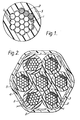
- Figure 2 shows a cable formed by laying together seven wires shown in figure 1, forming an electromagnetic interference screen 4 about the bundle by braiding and then extruding thereon a jacket 5 based on a halogen-free composition as described in British Patent Specification No. 2,068,347 Example lA.
- Figure 3 shows a flat conductor flat cable comprising an array of flat copper conductors 1 with a 100 mil (2.54 mm) spacing.
- Each copper conductor 1 is provided with a 3 micrometre thick aluminium intermediate layer (not shown) and a ferrite layer thereon as described above, both the aluminium and ferrite layers shown by reference numberal 2, and the coated conductors are embedded in a single polymeric insulating layer 3 formed for example from one of the polymers described with reference to figure 1.
- Fig. 4 Apparatus for use in a batch process for providing the keying layer on a wire conductor substrate by the sputtering method is illustrated in Fig. 4.
- the apparatus comprises a vacuum chamber into which a complete wire transport mechanism which includes wire pay-off reel 2 and take-up reel 3, wire support rolls 10 and tensioning rolls 11 is loaded.
- the mechanism engages motor drives which control the passage of wire 4 so that the wire traverses a vertically mounted target 5 a number of times. Deposition occurs by the processes previously described.
- An additional target (not shown) may be employed on the other side of the wire to increase coating rates and additional targets, e.g. target 6 can be employed to deposit intermediate layers before and/or after deposition of the primary coating.
- Suitable design of the gas inlet system to suit the specific geometries employed can facilitate deposition of layers which have no defined boundaries as described previously. Batch length will depend on chamber dimensions and transport system design.
- wire 4 is transferred from one reel 2 to the other 3 within the chamber.
- the route taken by the wire may cause it to pass before the smaller ancillary target 6 to deposit an intermediate layer of any desired material.
- Power to this target, combined with wire speed and the number of passes in front of the target will control the thickness of the intermediate layer deposit.
- the wire 4 may then pass in front of the larger primary target 5 to deposit the main coating. Again thickness will be dictated by a combination of power, wire speed and a number of passes.
- the ratio of thicknesses between the intermediate and the primary coating is controlled in the same way. Multi-layers can be built up by reversing the mechanism as desired such that the wire 4 passes back past the targets 5,6 in reverse order.
- Thickness and composition may be altered in the reverse pass as required, e.g. the process employed at the smaller magnetron may be reactive on the reverse pass to deposit a compound of the metal on the intermediate layer, e.g. Ti and Tio x .
- Deposition of layers with no defined boundary between the metal intermediate layers (or substrates) and the oxide coatings may be achieved by setting up gradients of reactive gas in front of the primary target, such that wire at the top edge of the target 5 is subjected to deposition in an Argon rich atmosphere which gradually increases in reactive gas content as the wire progresses down the face of the target.
- a gradient can be achieved by a baffle system (not shown) which progressively leaks oxygen introduced at the bottom end of the target towards the upper end.
- a graded metal flux to the substrate could be employed by interposing suitable shields between the target and the substrate.
- a simpler technique for producing the layer with no defined boundary involves use of a multipass process in which wire 4 is passed back and forth through the system, and with each pass the level of reactive gas is increased to a final level required to obtain the correct stoichiometry.
- the stoichiometry of the intermediate layer increases in a series of small incremental steps from metal to required stoichiometry.
- Composite targets may also be used to produce intermediate layers with stoichiometry gradients. In the case of discrete articles, the articles may instead be held in front of the target by means of a rotating sample holder.
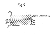
- Figure 5 is a schematic section through parts of an article according to the invention showing a typical arrangement of layers that may be formed on the copper substrate, the thickness of the layers being exaggerated for the sake of clarity.
- a copper substrate 21 is provided with a thick (e.g. 1 to 3 micrometres) layer 22 of nickel followed by a layer 23 of aluminium metal, the layer 23 having been formed e.g. by a sputtering method.
- An additional, layer 24 of ferrite or doped barium titanate (e.g. of about 5 to 15 micrometres thickness) has been deposited on the layer 23 by an appropriate method.
- an aluminium layer or an aluminium/nickel/copper composite layer may be formed on the barium titanate layer 24 to act as a second electrode.
- 19 strand, 22 AWG copper wire conductors were provided with a 4 micrometres thick titanium intermediate layer by use of the sputtering apparatus shown schematically in figure 4 of the drawings.
- the sputtering conditions were as follows: the wire 4 was precleaned by vapour degreasing in 1,1,1-trichloroethane prior to deposition. The cleaning was achieved by passing the wire through a vapour degreasing bath such that a residence time of 3 minutes was achieved. The wire 4 was then loaded into the vacuum chamber. The chamber was then evacuated to a pressure of lxio-6 mbar prior to starting the process.
- the titanium-coated wire was then coated with a substoichiometric oxide of titanium, TiO x , by reversing the wire handling mechanism and sputtering from the titanium target in an argon/oxygen atmosphere.
- TiO x a substoichiometric oxide of titanium
- bare copper wire with no Ti intermediate layer
- TiO x was also coated with TiO x . Both Ti and TiO x layers surrounded the bundles of copper strands, but not each individual strand.
- the samples were assessed for the adhesion of the TiO x layer, and the results are given in Table 1.
- Examples 1 and 2 The ability of Examples 1 and 2 to withstand thermal cycling was also tested. Square wave current pulses (30A, 60 seconds on, 30 seconds off) were repeatedly passed down the wire samples, which heated them from 25°C to 350°C and back again. The TiO x coating of example 1 was seen to spall away from the conductor after 1 cycle, whereas Example 2 remained completely intact even after 10 cycles.
- the electrical properties of the sputtered TiO x were investigated by coating a flat copper strip with 4pm Ti plus 4pm TiO x .
- the current/voltage relationship of the TiO x was measured using a variable voltage DC power supply and an ammeter, making contact to the TiO x film via an electrode made of silver-loaded conductive paint.
- a non-linear relationship between current and voltage was found, and the TiO x had a negative temperature coefficient of resistance (i.e. the TiO x was an NTC material).
- the resistivity of the TiO x film was found to be 7.10 7 ohm cm with an applied potential of 1V (lower with higher potential).
- Ni0 is an antiferromagnetic material at room temperature.
- Example 3 was also subjected to the thermal cycling test described above. Again, Example 3 (no Ni intermediate layer) was seen to spall after 1 cycle, but Example 4 (0.5pm Ni intermediate layer) was intact after 10 cycles.
- Examples 1-6 clearly demonstrate that the adhesion of inorganic metal compounds to metallic substrates can be significantly improved by the use of intermediate layers.
- Ni0- coated copper wire conductors identical to those of Example 3, were subsequently coated with substoichiometric titanium oxide, TiO x , as described in Example 1.
- TiO x substoichiometric titanium oxide
- the Ni0 was used as an intermediate layer, and not for its antiferromagnetic properties.
- These Cu-NiO-TiO x samples were found to be very robust compared with the wires of Example 1 (no Ni0 intermediate layer), and could be handled easily. They also survived 10 thermal cycles from room temperature to 250°C, while those of Example 1 spalled badly after only 1 cycle.
Landscapes
- Physical Vapour Deposition (AREA)
- Laminated Bodies (AREA)
- Thermistors And Varistors (AREA)
- Non-Insulated Conductors (AREA)
- Insulated Conductors (AREA)
- Communication Cables (AREA)
Abstract
Description
- This invention relates to electrical components, and in particular to components that include a conductive layer formed from an electrically conductive metal
- The present invention provides an electrical component which comprises a metallic electrical conductor and a conductive layer formed from an electrically conductive inorganic metal compound, the conductive layer being bonded to the electrical conductor by an intermediate metallic or refractory layer.
- The invention is applicable to many forms of electrical component in which an electrically conductive layer is provided in order to exhibit an electrical effect. The electrically conductive layer may be a semi-conductor or it may have a higher electrical conductivity, and may be either linear or non-linear in its electrical characteristics. For example in one form of device, the conductive layer may be formed from a material for example a doped ceramic such as an alkaline earth metal titanate, that exhibits a positive temperature coefficient of resistance (referred to hereinafter as a P.T.C. material) or it may exhibit a negative temperature coefficient of resistance (referred to hereinafter as an N.T.C. material). Such materials may have resistivities that vary through several orders of magnitude as the temperature of the material is raised through an interval of 10 to 50oC. Devices that utilise such P.T.C. materials may be used for instance as self limiting resistance heaters, circuit protection devices, electric motor start windings, contactless electrical switches and the like. In some applications the conductive layer may be formed from a ferroelectric material or from a ferromagnetic material or from other curie point materials. Electrical conductors that are coated with ferromagnetic materials may be used as high frequency attenuation lines in which unwanted high frequencies are attenuated, while components having ferroelectric coatings may be used for example as skin effect heaters. Examples of ferroelectric materials include those ceramics of the general formula AM03 wherein A represents lead or an alkaline earth metal, preferably barium or strontium, and M represents titanium, tin zirconium or hafnium; lithium niobate, lithium tantalate, lead titanate zirconate or lead metaniobate; and examples of ferromagnetic materials include ferrites, e.g. compounds of the general formula MFe204 wherein M represents for example iron (Fe304), nickel, cobalt or zinc; magnesium manganese ferrites and ferro- chromates; magnetic iron oxides such as gamma Fe203 or certain oxides of chromium or nickel. In yet other applications, the conductive layer may have a voltage dependent resistivity, for example in the case of zinc oxide varistors and vanadium oxide devices. Other forms of voltage dependent device that may be made according to this invention include threshold and memory switching devices that use chalcogenide glass layers e.g. germanium-arsenic-tellurium-silicon glasses as described for example in U.S. Patent Specification No. 3,271,591, the disclosure of which is incorporated herein by reference.
- As will be appreciated the above examples represent only a sample of the range of conductive layers that may be used for one reason or another in an electrical component.
- Although such components are very useful in many circumstances, they often suffer from the disadvantage that it is difficult for the conductive coating to adhere well to the underlying metallic conductor with the result that the component is unable to withstand severe mechanical abuse. In other cases, even if the conductive coating does adhere satisfactorily to the metallic conductor, the ability of the component to withstand high temperatures e.g. above 200°C or temperature cycling is severely limited. According to the present invention, however, the ability of the component to withstand mechanical abuse and/or temperature excursions may be significantly improved by the provision of an intermediate metallic or refractory layer. The preferred forms of intermediate layers used according to the present invention are as described in European Patent Specification No. 132343, the disclosure of which is incorporated herein by reference, and in our copending British Patent Applications Nos. 8500816 and 8500817 corresponding to European Patent Applications Nos. 85304871.8 and 85304872.6, the disclosures of which are also incorporated herein by reference. The conductive layer employed in the present invention may be present in place of the refractory coating or layer described in those applications or it may, if desired, be present in addition to a semiconducting or conducting refractory layer, e.g. a substoichiometric oxide, in which case the layer acts as a keying layer to improve the adhesion of the conductive layer.
- Preferably the metal from which the electrical conductor is formed has a melting point of at least 8000C more preferably at least 900°C, and especially at least 1000°C. The present invention is particularly applicable to articles in which the metal is copper or an alloy thereof for example wire and cable that may need to be capable of functioning when subjected to temp era- ture excursions, or even when subjected to temperatures of 2000C or above, for lengths of time.
- In certain forms of component according to the invention e.g. electrical wire, and especially one or more additional conducting layers may be provided on top of the conductive layer. The further layer or layers may be formed by the methods that give faster deposition rates such as those mentioned in our British Patent Application No. 8500818.
- In the case where the article comprises an electrical wire or cable, so that the underlying copper forms the conductor of the cable, the conductor may be a single, solid conductor or it may be a stranded conductor in which individual strands are laid together to form a bundle which preferably contains 7, 19 or 37 strands. Where the conductor is stranded it is preferred for the bundle to be coated rather than the individual strands, that is to say, the conductive coating extends around the circumference of the bundle but not around the individual strands so that substantially only the outwardly lying surfaces of the outermost layer of strands are coated. The intermediate layer may also extend around the bundle or, for example in the case of a nickel intermediate layer, may extend around the individual strands.
- This form of conductor has the advantage that the inter strand electrical contact is retained and the dimensions of the bundle are kept to a minimum (since the thickness of the coating may constitute a significant proportion of the strand dimensions for fine gauge conductors) and also it aids the formation of good electrical connections, e.g. crimp connections, to the conductor because a large proportion of the surface of the strands, and the entire surface of the strands in the central region of the conductor, will be uncoated by the layer. If a cable is formed according to the invention from a stranded conductor, it has the advantage that is it very flexible as compared with solid conductor wires and yet has sufficient electrical insulation provided by the outermost insulating refractory layer, as described in the above European Patent Specification.
- The thickness of the conductive and keying layers will depend on the application to which the component is put and the nature of the conductive layer.
- The properties of intermediate coatings are known to depend significantly on the method by which they are formed or deposited onto a substrate, and in general, the techniques that exhibit relatively low deposition rates will form layers having relatively high density, i.e. not being porous, and having higher adhesion to metallic substrates. Preferably the intermediate layer has been formed by a vacuum deposition process, e.g. a sputtering, evaporation, ion plating, or chemical vapour deposition process. Such methods are also appropriate and are preferred for forming the conductive layer although it may, if desired, be formed by other methods, e.g. plasma ashing methods, solution coating methods or flame spraying methods.
- In order to optimise the adhesion between the intermediate or keying layer and the conductive layer, it may be beneficial for the intermediate or keying layer to comprise the or one of the metals that is present in the conductive layer. Alternatively or in addition keying layers that are capable of supporting epitaxial growth of the conductive layer, e.g. spinels, may be used.
- As stated above, the intermediate layer may be formed from a metal or refractory. It is possible for the component to include more than one such layer and for the layers to be both metallic, both refractory or for a metallic and a refractory layer to be present. In order to improve further the high temperature properties of the component, and especially in the case where the underlying metal is copper or an alloy thereof, it is preferred for a metallic intermediate layer (hereinafter called the "additional layer") to be present between the intermediate layer and the metallic conductor. The metal is preferably one which forms a good bond between the underlying metal and the refractory keying layer and also, as described in our copending Application No. 8500816 one which acts as a barrier to diffusion of oxygen or copper or both or which acts to reduce stress in the refractory layers imposed by substrate strain resulting from mechanical or thermal stress. Preferred metallic intermediate or additional layers include those formed from aluminium, and alloys for example with magnesium, titanium, tantalum chromium, manganese, silicon or nickel although other metals may be used. In the case of wires having stranded conductors, it is preferably for the wire to have the structure as described in our Patent Application No. 8500817, i.e. one in which the additional layer may extend around the individual strands while the conductive layer extends around the conductor but not around the individual strands.
- In the case of wires according to the invention, polymeric insulation may be provided in order to provide additional insulation to the conductor during normal service conditions and also to enable the wire to have the desired dielectric properties and other properties e.g. mechanical properties, scuff resistance, colour coding ability etc. Such polymeric insulation is described in our patent applications referred to above.
- In some cases it may be desirable for the wire to be provided with a polymeric layer that contains conducting, semi-conducting or ferromagnetic particles (especially ferrites) or the like.
- As stated above, the preferred methods of forming the intermediate or keying layer include evaporation, plasma assisted chemical vapour deposition and sputtering methods.
- An advantage of using a relatively slow deposition method such as a sputtering method, for forming the intermediate or keying layer is that it allows greater control over the chemical composition and mechanical properties of the keying layer to be exercised. For example, it is often advantageous for the keying layer to be non-stoichiometric since this may increase the adhesion between the keying layer and any underlying layer, and especially if the stoichiometry of the keying layer varies through at least part of its thickness so that stresses that may be induced in the coating, for example due to differential thermal expansion, are not localised to a boundary of the layer and so that different parts of the layer will exhibit different properties. For example, a relatively metal-rich part of the keying layer may exhibit good adhesion to the conductor or additional intermediate layer while part of the coating having least metal or semi-metal may exhibit better adhesion to the conductive layer.
- If desired, the stoichiometry of the keying layer may vary continuously throughout the thickness of the layer or it may contain one or more layers or strata of relatively uniform stoichiometry. Thus the keying layer may have an outer region of relatively uniform stoichiometry in order to exhibit the optimum electrical properties or adhesion to the further refractory layer. The relative thicknesses of the non-uniform and uniform layers may vary widely. For example the major part of the keying may have a non-uniform stoichiometry or the major part of the layer's thickness may be of uniform stoichiometry, in which latter case the non-uniform part of the layer could even be considered as an intermediate layer that improves adhesion of the rest of the layer especially at high temperatures. If the underlying metal- or semi-metal-rich part of the keying layer is intended to improve the adhesion of the conducting coating, its particular composition will depend on the composition of any additional layer, and in some cases it may be desirable for the metal or semi-metal rich part to consist substantially entirely of the metal or semi-metal so that there is a gradual change from the metal or semi-metal to the composition of the conductive layer. This is particularly preferred if the system includes an underlying layer of the same metal or semi-metal.
- The precise stoichiometry of the uniform top layer can be determined experimentally using wavelength dispersive electron microprobe analysis or by using x-ray photoelectron spectroscopy (XPS). The composition of the coating as it changes from metal to refractory throughout its depth can be assessed using Auger electron spectroscopy (AES) in which the film is continuously sputtered away to expose fresh surface for composition analysis.
- The variation in stoichiometry is not limited to a variation in the metal or semi-metal/oxygen proportions. In addition or alternatively the relative proportions of two different metals or semi-metals may be varied so that, for example, there is a gradual change from one metal, which may constitute an intermediate layer, to the oxide of a different metal.
- In the sputtering method, predominantly neutral atomic or molecular species are ejected from a target, which may be formed from the material to be deposited, under the bombardment of inert gas positive ions e.g. argon ions. The high energy species ejected will travel considerable distances to be deposited on the wire conductor substrate held in a medium vacuum, e.g. 10-4 to 10-2 mbar. The positive ions required for bombardment may be generated in a glow discharge where the sputtering target serves as the cathode electrode to the glow discharge system. The negative potential (with respect to ground and the glow discharge) is maintained in the case of insulating target materials by the use of radio frequency power applied to the cathode, which maintains the target surface at a negative potential throughout the process. DC power may be applied when the target is an electrically conducting material. The advantage of such techniques is that control over the coating material is greatly enhanced, and the energy of the species ejected is very much higher than with evaporation methods e.g. typically 1 to 10 eV for sputtering as compared with 0.1 to 0.5 eV for evaporation methods. Considerable improvements in interfacial bonding are achieved but the deposition rate in the sputtering process described will be lower than that for electron beam evaporation.
- In magnetron sputtering processes the plasma is concentrated immediately in front of the cathode (target) by means of a magnetic field. The effect of the magnetic field on the gas discharge is dramatic. In that area of discharge where permanent magnets, usually installed behind the cathode, create a sufficiently strong magnetic field vertically to the electric field, secondary electrons resulting from the sputter bombardment process will be deflected by means of the Lorentz force into circular or helical paths. Thus the density of electrons immediately in front of the cathode as well as the number of ionised argon atoms bombarding the cathode are substantially increased. There is an increase in plasma density and a considerable increase in deposition rate. Bias sputtering (or sputter ion plating) may be employed as a variation of this technique. In this case the wire conductor is held at a negative potential relative to the chamber and plasma. The bombardment of the wire conductor by Argon ions results in highly cleaned surfaces. Sputtering of the target material onto the wire conductor thoughout this process results in a simultaneous deposition/cleaning mechanism. This has the advantage that the interfacial bonding is considerably improved. In sputter ion plating systems both target and the wire conductor are held at a negative potential. In this case the relative potentials are balanced to promote preferential sputtering of the target material. The target voltage will be typically less than lkV, dependent on system design and target material. The wire substrate, may be immersed in its own localised plasma dependent upon its bias potential, which will be lower than that of the target. The exact voltage/power relationship achieved at either target or substrate is dependant upon many variables and will differ in detail from system to system. Typical power densities on the target are 10-20W/cm2. The load to the substrate may be substantially lower, often as little as 5% of the target load.
- One preferred technique that is used to apply the conductive coating is a reactive bias sputtering method in which reactive gas is introduced into the vacuum chamber in addition to argon so that a compound of the target material, which in this case is a metal or semi metal rather than the compound itself, will be deposited. Experimental results have shown that the level of reactive gas and its admission rate have a significant effect on deposition rates. The precision control of partial pressure of the reactive gas and the analysis of the sputtering atmosphere in a closed loop control system is considered highly desirable. Apart from the simultaneous deposition/cleaning advantages mentioned above, the ion bombardment of the substrate enhances surface reaction between the reactive gas and depositing species, resulting in more efficient formation of the coating with the required stoichiometry.
- Partial pressure of reactive gas is determined experimentally but will normally be between 2 and 25% but sometimes up to 30%, the exact level depending on the required stoichiometry of the coating and depostion rate. Reactive sputtering is also a preferred technique because it facilitates alterations to the stoichiometry of the coating. For. example, an intermediate "layer" of the pure metal used for the conductive coating may be deposited in such a way that there is no defined boundary between the conductor metal, keying layer and conducting layer.
- The vacuum chambers and ancillary equipment, including micro-processor gas control units and a variety of targets used in these methods may be purchased commercially. Many variations in design are possible but most employ the use of "box" shaped chambers which can be pumped down to high vacuum for use in any of the vacuum deposition processes mentioned. Systems are normally, but not exclusively, dedicated to one deposition process. One system which may be employed to coat wire uses air to air transfer tech niques for passage of the wire conductor through the deposition chambers and employs one or more ancillary vacuum chambers either side of the main deposition chamber.
- These ancillary chambers are held at progressively higher pressures as they extend from deposition chamber to air. This reduces the load on individual vacuum seals. The system described has the advantage of con tinuous feed of the wire conductor over batch process arrangements. In the vacuum deposition chamber the pressure is held constant at a pressure normally between 10-4 and 10-2 Torr.
- The targets employed are commercially available Planar Magnetron Sputtering sources. Their size may vary widely, and targets in excess of 2 metres in length may be employed. Between two and four such sources may be arranged opposite one another so as to surround the wire conductor passing through the chamber or to sputter from at least two sides. The arrangement may be employed in series to increase wire throughput rates. As described above a negative bias is applied to the magnetron to initiate the sputtering process. The wire may be held at a lower negative bias as described earlier.
- Refinements to the system can, if desired, be employed. For example, the use of an intermediate vacuum station between the air (input side) and the deposition chamber may be employed to generate an Argon ion glow discharge which cleans the wire conductor suface by ion bombardment prior to its entry into the vacuum deposition chamber and also heats the wire conductor.
- Further intermediate chambers can be employed between the cleaning and deposition chamber to deposit intermediate layers.
- Conditions may be controlled to produce any of the conductor coatings described above in which no defined boundries occur between the layers. For example an additional, underlying "layer" of the pure metal used for the conducting coating may be deposited in such a way that there is no defined boundary between the conductor additional layer and the conducting coating. In a similar fashion additional chambers can be employed between the deposition chamber and air (output side) to deposit the conductive coating onto the intermediate layer and also any subsequent layers, e.g. for lubrication, wear resistance or the provision of additional electrodes.
- Evaporation and the related processes of activated evaporation and ion plating offer alternative techniques for deposition of the coating.
- Evaporation of the coating material is achieved by heating the material such that its vapour pressure exceeds 10-2mbar. Evaporation temperatures vary according to coating material, e.g. 1300-3500°C for refractory metal oxides, the chamber pressure being usually 10-4 to 10-6mbar. Similar wire transport systems to those described may be used to hold the substrate about 30-40 cm above the source. Several heating methods exist e.g. resistive, inductive, electron beam impingement etc. although the preferred method is an electron beam source where a beam of high energy electrons e.g. 10,000eV impinge onto the coating material contained in a water-cooled crucible. The use of multi-pot crucibles or twin source guns, enable multiple layers and graded stoichiometry layers to be deposited with the aid of electronic monitoring and control equipment.
- Compound coatings can be made either by direct evaporation from that compound e.g. TiN or by reactive evaporation, e.g. titanium evaporated into a partial pressure of nitrogen to give titanium nitride. Variations in the process exist either to promote reactions or adhesion, e.g. Activated reactive evaporation (ARE) can be used to increase the reaction probably between the evaporant and the reactive gas.
- In ion-plating, negative bias applied to the substrate in an inert gas promotes simultaneous cleaning/deposition mechanisms for optimising adhesion as described in the sputtering process. Bias levels of -2kV are typically used but these can be reduced to suit wire substrates. Alternatively, high bias can be applied to a plate positioned behind the traverse wire to achieve a similar effect. As operating pressures are higher in the ion plating technique, e.g. 10-3 to 10-2mbar, gas scattering results in a more even coating distribution. To protect the filament the electron beam gun in the ion plating technique is differentially pumped to maintain vacuum higher than 10-4mbar.
- In the Plasma assisted chemical vapour deposition (PACVD) method the substrate to be coated is immersed in a low pressure (0.1 to 10 Torr) plasma of the appropriate gases/volatile compounds. This pressure is maintained by balancing the total gas flow-rate against the throughput of the pumping system. The plasma is electrically activated and sustained by coupling the energy from a power generator through a matching network into the gas medium. Thin films have been successfully deposited from direct current and higher. frequency plasmas well into the microwave range. At high frequencies the energy may be capacitatively or inductively coupled depending on chamber.design and electrode configuration. Typically a 13.56 MHz radio-frequency generator would be used having a rating which would allow a power density of between 0.1 - lOW/cm2 in a capacitatively-coupled parallel-plate type reactor. The substrate, which could be set at a temperature of up to 400°C, may be grounded, floating or subjected to a dc voltage bias as required. Typically deposition rates for this technique can be favourably compared with those obtained by sputtering.
- After the keying layer has been formed, the conductive layer is applied. As stated above, many of the methods for forming the intermediate or keying layer may be used for forming the conductive layer, or other methods may be used instead. Reactive sputtering, evaporation and chemical vapour deposition are preferred methods although faster deposition methods may be used.
- After the keying layer and conductive refractory layer have been deposited on the wire conductor it may be desirable to coat the layer with a thin coating of a polymeric resin or lacquer in order to provide mechanical protection and a barrier against water or electrolytes during service. Further conductive particle loaded polymer and/or polymeric insulation may then be extruded onto the coated conductor by methods well known in the art.
- In order to form a cable, the appropriate wires according to the invention may simply be laid together and be enclosed in a jacket. If desired the wires may be provided with a screen or electromagnetic interference shield before the cable jacket is applied. Thus a cable may be formed in a continuous process by means well known in the art by braiding the wire bundle and extruding a cable jacket thereon. Any of the materials described above for the wire polymeric insulation may be used although halogen-free compositions e.g. compositions as described in the U.K. Patent Specifications Nos. 1,603,205 and 2,068,347A mentioned above are preferred. It is of course possible to employ additional means for providing integrity of the cable such as mica tape wraps, but these are not necessary nor are they desirable in view of the increased size and weight of the cable.
- Several embodiments of the invention and a method of production thereof will now be described by way of example with reference to the accompanying drawings in which:
- Figure 1 is a cross-section through one form of wire according to the present invention;
- Figure 2 is a cross-section through a cable employing the wires of figure 1;
- Figure 3 is a cross-section through part of a flat conductor flat cable;
- Figure 4 is a schematic view of part of the sputtering apparatus showing its wire handling mechanism; and
- Figure 5 is a schematic section through part of the thickness of component in accordance with the invention.
- Referring to figure 1 of the drawings, a 26 AWG stranded copper conductor formed from 19 copper strands is coated with a 3 micrometre thick intermediate or keying layer of aluminium by the sputter ion plating method described above, followed by a ferrite conductive layer for attenuation of unwanted high frequency signals, both layers being indicated by
reference numeral 2. Acoating 3 based on a polyetherimide or a polyether ether ketone or polyether ketone or an ETFE copolymer is then extruded on the oxide coated conductor to form a polymeric insulating layer of mean wall thickness 0.2 mm. - Figure 2 shows a cable formed by laying together seven wires shown in figure 1, forming an
electromagnetic interference screen 4 about the bundle by braiding and then extruding thereon ajacket 5 based on a halogen-free composition as described in British Patent Specification No. 2,068,347 Example lA. - Figure 3 shows a flat conductor flat cable comprising an array of flat copper conductors 1 with a 100 mil (2.54 mm) spacing. Each copper conductor 1 is provided with a 3 micrometre thick aluminium intermediate layer (not shown) and a ferrite layer thereon as described above, both the aluminium and ferrite layers shown by
reference numberal 2, and the coated conductors are embedded in a single polymeric insulatinglayer 3 formed for example from one of the polymers described with reference to figure 1. - Apparatus for use in a batch process for providing the keying layer on a wire conductor substrate by the sputtering method is illustrated in Fig. 4. The apparatus comprises a vacuum chamber into which a complete wire transport mechanism which includes wire pay-
off reel 2 and take-upreel 3, wire support rolls 10 and tensioning rolls 11 is loaded. The mechanism engages motor drives which control the passage ofwire 4 so that the wire traverses a vertically mounted target 5 a number of times. Deposition occurs by the processes previously described. As before, variations in set-up are possible. An additional target (not shown) may be employed on the other side of the wire to increase coating rates and additional targets,e.g. target 6 can be employed to deposit intermediate layers before and/or after deposition of the primary coating. Suitable design of the gas inlet system to suit the specific geometries employed can facilitate deposition of layers which have no defined boundaries as described previously. Batch length will depend on chamber dimensions and transport system design. - In the operation of such a
batch process wire 4 is transferred from onereel 2 to the other 3 within the chamber. The route taken by the wire may cause it to pass before the smallerancillary target 6 to deposit an intermediate layer of any desired material. Power to this target, combined with wire speed and the number of passes in front of the target will control the thickness of the intermediate layer deposit. Thewire 4 may then pass in front of the largerprimary target 5 to deposit the main coating. Again thickness will be dictated by a combination of power, wire speed and a number of passes. The ratio of thicknesses between the intermediate and the primary coating is controlled in the same way. Multi-layers can be built up by reversing the mechanism as desired such that thewire 4 passes back past thetargets target 5 is subjected to deposition in an Argon rich atmosphere which gradually increases in reactive gas content as the wire progresses down the face of the target. A gradient can be achieved by a baffle system (not shown) which progressively leaks oxygen introduced at the bottom end of the target towards the upper end. Alternatively, a graded metal flux to the substrate could be employed by interposing suitable shields between the target and the substrate. - A simpler technique for producing the layer with no defined boundary involves use of a multipass process in which
wire 4 is passed back and forth through the system, and with each pass the level of reactive gas is increased to a final level required to obtain the correct stoichiometry. Thus the stoichiometry of the intermediate layer increases in a series of small incremental steps from metal to required stoichiometry. Composite targets may also be used to produce intermediate layers with stoichiometry gradients. In the case of discrete articles, the articles may instead be held in front of the target by means of a rotating sample holder. - Figure 5 is a schematic section through parts of an article according to the invention showing a typical arrangement of layers that may be formed on the copper substrate, the thickness of the layers being exaggerated for the sake of clarity.
- A
copper substrate 21 is provided with a thick (e.g. 1 to 3 micrometres) layer 22 of nickel followed by alayer 23 of aluminium metal, thelayer 23 having been formed e.g. by a sputtering method. An additional,layer 24 of ferrite or doped barium titanate (e.g. of about 5 to 15 micrometres thickness) has been deposited on thelayer 23 by an appropriate method. - Although the layers are clearly demarcated in the drawing by means of lines, it will be appreciated that such boundaries may not, and preferably will not, be formed in practice, especially between the copper/aluminium layers.
- If desired, further layers may be formed on the article as appropriate. For example an aluminium layer or an aluminium/nickel/copper composite layer may be formed on the
barium titanate layer 24 to act as a second electrode. - The following Examples illustrate the invention:
- 19 strand, 22 AWG copper wire conductors were provided with a 4 micrometres thick titanium intermediate layer by use of the sputtering apparatus shown schematically in figure 4 of the drawings. The sputtering conditions were as follows: the
wire 4 was precleaned by vapour degreasing in 1,1,1-trichloroethane prior to deposition. The cleaning was achieved by passing the wire through a vapour degreasing bath such that a residence time of 3 minutes was achieved. Thewire 4 was then loaded into the vacuum chamber. The chamber was then evacuated to a pressure of lxio-6 mbar prior to starting the process. At this stage argon was admitted to attain a pressure of 1.5 x 10⁻² mbar whereupon a high frequency (80 kHz) bias potential was applied to the wire handling system which was isolated from ground. A bias potential of -850V was achieved, and the wire was transferred fromreel 3 to reel 2 such that a residence time of 10 minutes was achieved. On completion of the cleaning cycle the pressure was reduced to 8.10-3 mbar and the deposition process started. - 4kW of DC power was applied to the
titanium target 5. The wire passed fromreel 2 to reel 3 being coated as it passed thetarget 5. Residence time in this region was controlled by wire speed and adjusted to give the required thickness. The roller mechanism alternated the wire face exposed to the target as it progressed down the target length. - The titanium-coated wire was then coated with a substoichiometric oxide of titanium, TiOx, by reversing the wire handling mechanism and sputtering from the titanium target in an argon/oxygen atmosphere. By way of comparison, bare copper wire (with no Ti intermediate layer) was also coated with TiOx. Both Ti and TiOx layers surrounded the bundles of copper strands, but not each individual strand. The samples were assessed for the adhesion of the TiOx layer, and the results are given in Table 1.

- The ability of Examples 1 and 2 to withstand thermal cycling was also tested. Square wave current pulses (30A, 60 seconds on, 30 seconds off) were repeatedly passed down the wire samples, which heated them from 25°C to 350°C and back again. The TiOx coating of example 1 was seen to spall away from the conductor after 1 cycle, whereas Example 2 remained completely intact even after 10 cycles.
- The results show that the Ti intermediate layer significantly improves the adhesion of the TiOx to the copper wire.
- The electrical properties of the sputtered TiOx were investigated by coating a flat copper strip with 4pm Ti plus 4pm TiOx. The current/voltage relationship of the TiOx was measured using a variable voltage DC power supply and an ammeter, making contact to the TiOx film via an electrode made of silver-loaded conductive paint. A non-linear relationship between current and voltage was found, and the TiOx had a negative temperature coefficient of resistance (i.e. the TiOx was an NTC material). The resistivity of the TiOx film was found to be 7.107 ohm cm with an applied potential of 1V (lower with higher potential).
- 19 strand, 22 AWG copper wire conductors were coated with layers of Ni and Ni0 as shown in Table 2. The sputtering method described above was used to manufacture these samples. Ni0 is an antiferromagnetic material at room temperature.
- The samples were then tested to determine the adhesion of the top coat as follows. A fixed length of wire was subjected to a tensile stress whilst the strain was continuously recorded. During testing the wire sample was viewed through an optical microscope. When the coating was seen to spall significantly the strain was recorded. The strain value recorded at this point gave a measure of the adhesion at the coating. The results of this adhesion testing are also given in Table 2.
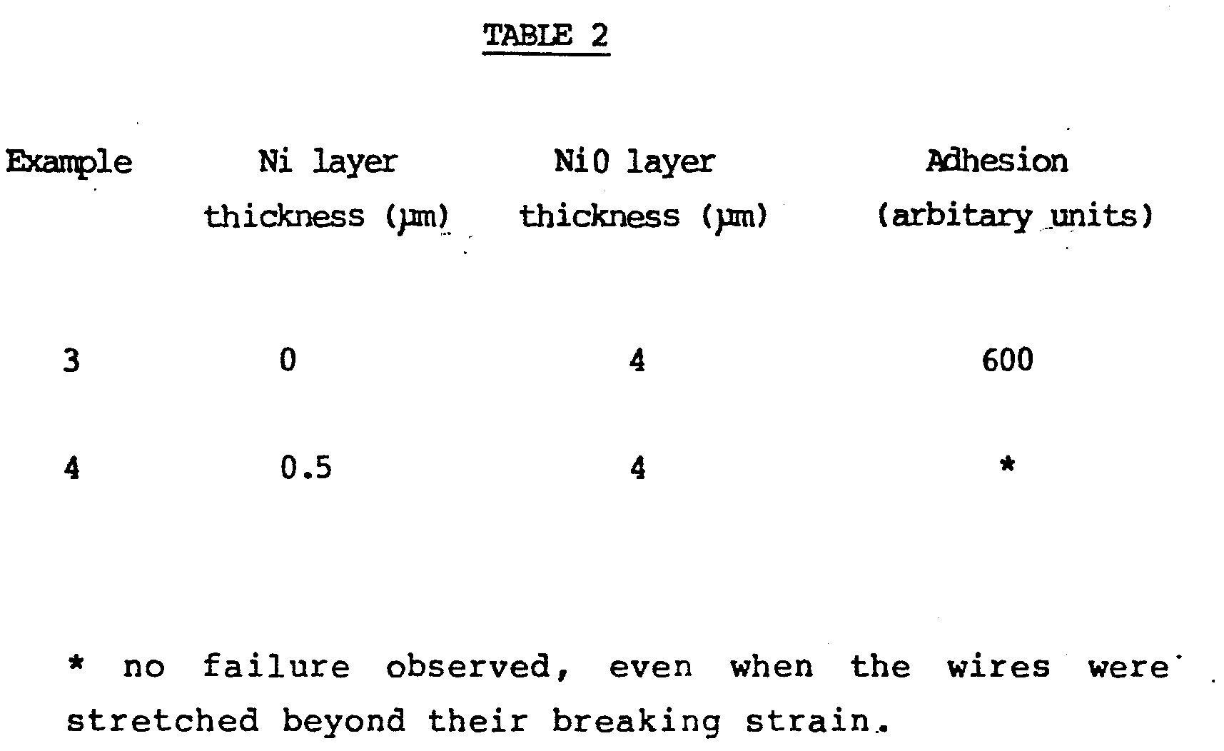
- Examples 3 and 4 were also subjected to the thermal cycling test described above. Again, Example 3 (no Ni intermediate layer) was seen to spall after 1 cycle, but Example 4 (0.5pm Ni intermediate layer) was intact after 10 cycles.
- Flat copper conductors were sputter coated with a 4um titanium intermediate layer, and subsequently coated with Si-doped barium titanate by thermal evaporation. The evaporation process used was as follows: pieces of Si-doped barium titanate were loaded into a molybdenum crucible, and the vacuum chamber pumped down to about 10-4 mbar. The power supply to the crucible was then switched on, heating the evaporant. When the heating current reached about 280A, the charge started to evaporate. Heating was continued for about 12 minutes, during which time Si-doped BaTi03 was deposited onto the Ti-coated copper substrates (which were held about 20cm above the crucible). Using this method, films about 0.3pm thick were deposited. To form a comparison, bare copper substrates (with no Ti intermediate layer) were also coated.
- The adhesion of the Si-doped BaTi03 films was tested by heating the coated flat conductors to about 500°C for 1 minute. On cooling, the titanate film had spalled away from the bare copper substrates, exposing copper that had oxidised in places. In contrast, those samples provided with the 4 µm Ti intermediate layer remained undamaged.
- Examples 1-6 clearly demonstrate that the adhesion of inorganic metal compounds to metallic substrates can be significantly improved by the use of intermediate layers.
- Ni0- coated copper wire conductors, identical to those of Example 3, were subsequently coated with substoichiometric titanium oxide, TiOx, as described in Example 1. In this instance, the Ni0 was used as an intermediate layer, and not for its antiferromagnetic properties. These Cu-NiO-TiOx samples were found to be very robust compared with the wires of Example 1 (no Ni0 intermediate layer), and could be handled easily. They also survived 10 thermal cycles from room temperature to 250°C, while those of Example 1 spalled badly after only 1 cycle.
Claims (15)
Applications Claiming Priority (2)
| Application Number | Priority Date | Filing Date | Title |
|---|---|---|---|
| GB858502316A GB8502316D0 (en) | 1985-01-30 | 1985-01-30 | Electrical components |
| GB8502316 | 1985-01-30 |
Publications (2)
| Publication Number | Publication Date |
|---|---|
| EP0190888A2 true EP0190888A2 (en) | 1986-08-13 |
| EP0190888A3 EP0190888A3 (en) | 1986-11-20 |
Family
ID=10573657
Family Applications (1)
| Application Number | Title | Priority Date | Filing Date |
|---|---|---|---|
| EP86300654A Withdrawn EP0190888A3 (en) | 1985-01-30 | 1986-01-30 | Electrical component |
Country Status (4)
| Country | Link |
|---|---|
| EP (1) | EP0190888A3 (en) |
| JP (1) | JPS61185812A (en) |
| CA (1) | CA1256173A (en) |
| GB (1) | GB8502316D0 (en) |
Cited By (1)
| Publication number | Priority date | Publication date | Assignee | Title |
|---|---|---|---|---|
| WO2005008682A1 (en) * | 2003-07-03 | 2005-01-27 | Infineon Technologies Ag | Electrically conducting element comprising an adhesive layer, and method for depositing an adhesive layer |
Families Citing this family (3)
| Publication number | Priority date | Publication date | Assignee | Title |
|---|---|---|---|---|
| CA2116358A1 (en) * | 1991-09-27 | 1993-04-01 | Harry A. Loder | An improved ribbon cable construction |
| TW198118B (en) * | 1991-09-27 | 1993-01-11 | Minnesota Mining & Mfg | |
| JP5974764B2 (en) * | 2012-08-31 | 2016-08-23 | 小林 博 | Manufacturing and manufacturing method of fire-resistant layer of heat- and fire-resistant insulated electric wire or cable |
Family Cites Families (4)
| Publication number | Priority date | Publication date | Assignee | Title |
|---|---|---|---|---|
| FR2088188B1 (en) * | 1970-05-26 | 1974-08-09 | Honeywell Bull Soc Ind | |
| CH527488A (en) * | 1971-07-29 | 1972-08-31 | Alusuisse | Method for manufacturing a busbar |
| DE3123357A1 (en) * | 1981-06-12 | 1982-12-30 | Degussa Ag, 6000 Frankfurt | "ELECTRICAL CONTACT" |
| GB8318612D0 (en) * | 1983-07-08 | 1983-08-10 | Raychem Ltd | Wire and cable |
-
1985
- 1985-01-30 GB GB858502316A patent/GB8502316D0/en active Pending
-
1986
- 1986-01-29 CA CA000500568A patent/CA1256173A/en not_active Expired
- 1986-01-30 EP EP86300654A patent/EP0190888A3/en not_active Withdrawn
- 1986-01-30 JP JP61020039A patent/JPS61185812A/en active Pending
Cited By (1)
| Publication number | Priority date | Publication date | Assignee | Title |
|---|---|---|---|---|
| WO2005008682A1 (en) * | 2003-07-03 | 2005-01-27 | Infineon Technologies Ag | Electrically conducting element comprising an adhesive layer, and method for depositing an adhesive layer |
Also Published As
| Publication number | Publication date |
|---|---|
| GB8502316D0 (en) | 1985-02-27 |
| JPS61185812A (en) | 1986-08-19 |
| EP0190888A3 (en) | 1986-11-20 |
| CA1256173A (en) | 1989-06-20 |
Similar Documents
| Publication | Publication Date | Title |
|---|---|---|
| US4985313A (en) | Wire and cable | |
| US5209987A (en) | Wire and cable | |
| EP0132343B1 (en) | Wire and cable | |
| EP0940481B1 (en) | Method and apparatus for forming a thin film of a metal compound | |
| US5742471A (en) | Nanostructure multilayer dielectric materials for capacitors and insulators | |
| US4420385A (en) | Apparatus and process for sputter deposition of reacted thin films | |
| US3749658A (en) | Method of fabricating transparent conductors | |
| EP0188369B1 (en) | Refractory coated article | |
| JPH01144518A (en) | Long-sized superconductor and manufacture thereof | |
| EP0190888A2 (en) | Electrical component | |
| EP0170440B1 (en) | Temperature resistant coated wire | |
| EP0170441B1 (en) | Electrical wire and cable | |
| CN119855935A (en) | Conductive sputter target and method for depositing a layer using the same | |
| GB2183080A (en) | Coated electrical conductor | |
| GB2183079A (en) | Coated metallic conductor | |
| GB2182800A (en) | A flat cable | |
| JP3079765B2 (en) | Materials for electrical contacts | |
| Avrekh et al. | Transparent, conducting, metallic thin films | |
| JPS61502710A (en) | Heat-resistant coated articles | |
| KR0141509B1 (en) | Method for zinc adhesive strength film | |
| CA1268241A (en) | Electric insulation thin layer containing carbon | |
| Khan | Sputter deposition of dielectric films using a magnetic field for protection from high energy electrons | |
| JP3060709B2 (en) | Method and apparatus for manufacturing electrical contact material | |
| JPH0243357A (en) | Production of thin superconducting film | |
| Tokumaru et al. | High resistivity AlOx thin films deposited by a novel two-step sputtering process |
Legal Events
| Date | Code | Title | Description |
|---|---|---|---|
| PUAI | Public reference made under article 153(3) epc to a published international application that has entered the european phase |
Free format text: ORIGINAL CODE: 0009012 |
|
| 17P | Request for examination filed |
Effective date: 19860204 |
|
| AK | Designated contracting states |
Kind code of ref document: A2 Designated state(s): AT BE CH DE FR GB IT LI NL SE |
|
| PUAL | Search report despatched |
Free format text: ORIGINAL CODE: 0009013 |
|
| AK | Designated contracting states |
Kind code of ref document: A3 Designated state(s): AT BE CH DE FR GB IT LI NL SE |
|
| 17Q | First examination report despatched |
Effective date: 19871027 |
|
| STAA | Information on the status of an ep patent application or granted ep patent |
Free format text: STATUS: THE APPLICATION HAS BEEN WITHDRAWN |
|
| 18W | Application withdrawn |
Withdrawal date: 19930127 |
|
| APAF | Appeal reference modified |
Free format text: ORIGINAL CODE: EPIDOSCREFNE |
|
| RIN1 | Information on inventor provided before grant (corrected) |
Inventor name: SMITH, NICHOLAS JOHN G. Inventor name: PENNECK, RICHARD JOHN Inventor name: O'BRIEN, JAMES MARTIN |