EP0189676A1 - Driving circuit for brushless DC motors - Google Patents
Driving circuit for brushless DC motors Download PDFInfo
- Publication number
- EP0189676A1 EP0189676A1 EP85309487A EP85309487A EP0189676A1 EP 0189676 A1 EP0189676 A1 EP 0189676A1 EP 85309487 A EP85309487 A EP 85309487A EP 85309487 A EP85309487 A EP 85309487A EP 0189676 A1 EP0189676 A1 EP 0189676A1
- Authority
- EP
- European Patent Office
- Prior art keywords
- circuit
- producing
- currents
- instruction signal
- motor
- Prior art date
- Legal status (The legal status is an assumption and is not a legal conclusion. Google has not performed a legal analysis and makes no representation as to the accuracy of the status listed.)
- Granted
Links
Images


Classifications
-
- H—ELECTRICITY
- H02—GENERATION; CONVERSION OR DISTRIBUTION OF ELECTRIC POWER
- H02P—CONTROL OR REGULATION OF ELECTRIC MOTORS, ELECTRIC GENERATORS OR DYNAMO-ELECTRIC CONVERTERS; CONTROLLING TRANSFORMERS, REACTORS OR CHOKE COILS
- H02P6/00—Arrangements for controlling synchronous motors or other dynamo-electric motors using electronic commutation dependent on the rotor position; Electronic commutators therefor
- H02P6/04—Arrangements for controlling or regulating the speed or torque of more than one motor
-
- H—ELECTRICITY
- H02—GENERATION; CONVERSION OR DISTRIBUTION OF ELECTRIC POWER
- H02P—CONTROL OR REGULATION OF ELECTRIC MOTORS, ELECTRIC GENERATORS OR DYNAMO-ELECTRIC CONVERTERS; CONTROLLING TRANSFORMERS, REACTORS OR CHOKE COILS
- H02P6/00—Arrangements for controlling synchronous motors or other dynamo-electric motors using electronic commutation dependent on the rotor position; Electronic commutators therefor
- H02P6/10—Arrangements for controlling torque ripple, e.g. providing reduced torque ripple
Definitions
- the present invention relates to a driving circuit for driving brushless DC motors.
- Brushless DC motors recently available frequently make use of Hall effect devices as rotor position detectors. As is well known, Hall effect devices widely vary in sensitivity. For this reason, various circuit techniques have been employed to accommodate such sensitivity variations. Further, many attempts have been made to reduce torque ripples of brushless DC motors.
- reference 1 discloses a typical technique that uses three Hall effect devices as rotor position detectors.
- the scheme of the driving circuit disclosed in reference 1 is not described in detail herein, but, the operation of the driving circuit is characterized in that the coils are switched at such timings that the signals from the Hall effect devices become zero so as to be less affected by the sensitivity variations among the devices. Further, the operation is characterized in that the electric currents supplied to the coils are partially modulated in response to a signal synchronized with the rotation of the motor for canceling out the torque ripples.
- the driving apparatus disclosed in the aforementioned reference 1 operates based on the timings at which the signals from the Hall effect devices become zero. This offers the advantage that the driving circuit is insusceptible to the sensitivity variations among the Hall effect devices.
- the driving circuit since the armature coils are alternately energized and deenergized, filter circuits containing relatively large capacitors for reducing the spike-like voltage produced by the switching of the coils need to be provided at the power supply terminals to the coils.
- the driving circuit has the disadvantage that it is likely to produce vibration and noise, because the electric currents flowing into the coils are suddenly caused to cease and commence.
- a driving circuit for a brushless DC motor comprises: a magnetic pole position detecting circuit for detecting positions of magnetic poles of a rotor magnet of the motor and delivering polyphase signals indicative of the positions; a rectifier adder circuit for producing a sum of positive or negative portions of the polyphase signals from the magnetic pole position detecting circuit; an instruction signal producing circuit for producing a torque instruction signal instructing a torque to be produced by the motor; a first error amplifier for adjusting a gain of the magnetic pole position detecting circuit to make an output signal of the rectifier adder circuit to be proportional to the torque instruction signal; a power supply circuit responsive to the polyphase signals for supplying currents to polyphase armature coils; current detecting means for detecting the currents supplied to the armature coils; a modulating signal producing circuit for modulating the currents supplied to the armature coils; and a second error amplifier for adjusting a gain of the power supply circuit to make an output signal of the current detecting means equal to an
- the magnetic pole position detecting circuit may comprises rotor position detector devices, buffer amplifiers and subtractors. Output signals from the detector devices are amplified by the buffer amplifiers, and difference signals between two of output signals of the buffer amplifiers X are produced by the subtractor circuits.
- the rectifier adder circuit produces the sum of positive or negative portions of the difference signals from the subtractor circuits.
- the output signal of the rectifier adder circuit is controlled to be a constant value proportional to the torque instruction signal.
- the torque instruction signal may be an externally given signal.
- the electric currents supplied to polyphase armature coils are converted into a voltage which is so controlled as to coincide with a modulating signal synchronized with the rotation of the motor. More specifically, the currents supplied to the armature coils are so modulated as to have a phase reversed from that of the torque ripples remaining in the motor. This can cancel low-order components of the torque ripples, whereby a circuit for driving a brushless DC motor showing little torque ripples can be obtained.
- the position signals from the position detecting circuit are amplified by the power supply circuit and then supplied to the polyphase armature coils. Therefore, each of the supplied current signals has a sinusoidal waveform. Thus, energization of the coils is not controlled by sudden switching action. Hence, no spike-like voltage (which would normally be caused by switching of electric current) is generated. This can dispense with a filter circuit which has a relatively large capacitor for reducing such spike-like voltage.
- Fig. 2 is a perspective view of a main portion of an electric motor to which the invention is preferably applied.
- This motor has a rotating shaft 7 mounting thereon a disk 8 made of soft iron which serves as a back yoke.
- a disklike rotor magnet 9 is rigidly fixed to the bottom surface of the disk 8 to constitute a rotor.
- Three-phase armature coils 4, 5, 6 are mounted on a stator 10 made of a soft iron plate.
- the shaft 7 is rotatably held by a bearing 11 that is secured to the stator 10 at a position surrounded by the coils 4, 5, 6.
- Hall effect devices 1, 2, 3 are disposed at the centers of the coils 4, 5, 6, respectively, and used to detect a position of the rotor by detecting a magnetic field generated by the rotor magnet 9.
- Fig. 1 is a circuit diagram showing an example of driving circuit according to the invention.
- the driving circuit has a magnetic pole position detecting circuit 110 that detects positions of magnetic poles of the rotor magnet 9 and delivers three-phase signals indicating the positions.
- the detecting circuit 110 has a DC power supply 20 for supplying a voltage to the three Hall effect devices 1, 2, 3.
- Buffer amplifiers 21, 22, 23 are provided after the Hall effect devices 1, 2, 3, respectively.
- the amplifiers 21-23 respectively convert differential output signals from the Hall effect devices 1-3 into currents i H1 , i H2 , i H3 , which are proportional to the differential output signals.
- Each of the amplifiers 21-23 delivers three output currents of same magnitude.
- the detecting circuit 110 further includes subtractor circuits 31, 32, 33.
- Each of the subtractor circuits 31, 32, 33 produces two output currents of same magnitude.
- the electric currents i P1 , i P2 , ip 3 produced by the subtractor circuits 31, 32, 33, respectively, are applied to power supply circuits 101, 102, 103, respectively.
- the other output currents of the subtractor circuits 31, 32, 33 are supplied to a rectifier adder circuit 40 consisting of diodes 41, 42, 43 and a resistor 44.
- the circuit 40 allows only the positive portions of the output currents i P1 , ip 2 , ip 3 of the subtractor circuits 31, 32, 33 to be applied to the resistor 44 to thereby produce a voltage corresponding to a sum of the rectified currents.
- An instruction signal producing circuit 80 has two output terminals at each of which an electric current (torque instruction signal) i T proportional to a signal E T instructing a torque appears.
- One output current i T is applied to a resistor 82 so as to be converted into a voltage which is applied to one input terminal of a first error amplifier 50.
- the other input terminal of the amplifier 50 receives the sum of the rectified currents from the rectifier adder circuit 40.
- the first error amplifier 50 adjusts gains of the amplifiers 21-23 in such a way that the two input voltages applied thereto become equal to each other.
- a modulating signal producing circuit 120 receives the currents i H1 , i H2 , i H3 from the buffer amplifiers 21, 22, 23 and the torque instruction signal i T from the instruction signal producing circuit 80, and delivers a modulating signal i.
- the circuit 120 is composed of an absolute value adder circuit 60 for converting the currents i H1 , i H2' i H3 into absolute values and summing up them, and a combining circuit for delivering the modulating signal i c which is a difference between the instruction signal i T from the circuit 80 and an output current i from the adder circuit 60.
- the three-phase armature coils 4, 5, 6 are connected in Y (star) and respectively supplied with output currents i 1 , i 2 , i3 of the power supply circuits 101, 102, 103, respectively.
- the input operating points of the circuits 101-103 are determined by a DC power supply 114.
- Resistors 111, 112 and 113 are provided to respectively change the output currents ip l , ip 2 , ip 3 of the subtractor circuits 31, 32, 33 into voltages.
- a resistor (R cs ) 90 is used to detect the currents i 1 , i 2' i3 supplied to the coils 4, 5, 6 as voltages.
- a second error amplifier 70 has two input terminals to one of which a voltage detected by the resistor 90 is applied.
- the modulating signal produced by the modulating signal producing circuit 120 is applied to the other input terminal.
- the second error amplifier 70 adjusts gains of the three power supply circuits 101, 102, 103 in such a way that the two input voltages applied to the second error amplifier 70 become equal to each other.
- the operation of the driving circuit for a brushless DC motor constructed as described above will next be described with reference to Figs. 3, 4, 5.
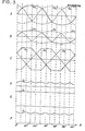
- Fig. 3 shows rotating angle 6 of the rotor in terms of electrical angle and waveforms appearing at specified portions in the driving circuit shown in Fig. 1.
- A shows waveforms of the differential output voltages e H1 , e H2 , e H3 from the Hall effect devices 1, 2, 3.
- the voltage e H2 lags relative to the voltage e H1 by 120°.
- the voltage e H3 lags relative to the voltage e H2 by 120°. It is assumed that the Hall effect devices 1, 2, 3 do not differ in sensitivity and that they show no offset.
- motors of permanent magnet rotor type have their permanent magnets magnetized in the form of trapezoidal wave in order to enhance the efficiency and productivity of the motors. Therefore, the differential output voltages from the Hall effect devices acting to detect the magnetic field contain harmonic components up to higher orders. In the example shown in A, components of the third, fifth and seventh orders account for 12.6%, 2.5% and 0.6%, respectively, of the fundamental wave.
- B shows waveforms of the output currents i H1 , i H2 , i H3 of the buffer amplifiers 21, 22, 23, and C shows waveforms of the output currents ip l , i P2 , ip 3 of the subtractor circuits 31, 32, 33.
- the buffer amplifiers 21, 22, 23, the subtractor circuits 31, 32, 33, the rectifier adder circuit 40, and the first error amplifier 50 constitute a control loop
- the peak values of the output currents i P1 , i P2 , i P3 of the subtractor circuits 31, 32, 33 become a constant value proportional to the instruction signal i c (F in Fig. 3) given to the motor.
- the aforementioned control loop operates to adjust the gains of the buffer amplifiers to maintain constant the peak values of the output currents i P1 , ip 2 , i P3 of the subtractor circuits 31, 32, 33.
- D shows a waveform of the output current i r of the absolute value adder circuit 60.
- the output current i r of the absolute value adder circuit 60 is expressed as:
- E shows the output current i T of the instruction signal producing circuit 80.
- the amplitude of the current i T is in proportion to the instruction signal given to the motor.
- F shows the current i c flowing into the resistor 71.
- the waveform of the current i c contains ripples of the sixth order.
- the power supply circuits 101, 102, 103, the resistor 90 for converting the electric currents flowing into the armature coils 4, 5, 6 into voltages, and the second error amplifier 70 constitute the control loop.
- the second error amplifier 70 is applied with the voltage developed by the resistor 90 and the voltage produced by the resistor 71, and adjusts the gains of the power supply circuits 101-103.
- the operation of the control loop will next be described by referring to Figs. 4 and 5.
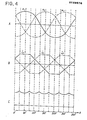
- Fig. 4 shows waveforms when the output terminal of the absolute value adder circuit 60 is open-circuited.
- A shows waveforms of the three-phase voltages e l , e 2 , e 3 which are induced in the three-phase armature coils 4, 5, 6, respectively, by the rotation of the rotor magnet of the motor.
- the voltage e 2 lags relative to e l by 120°, and e 3 lags relative to e 2 by 120°.
- the voltages e l , e 2 , e 3 respectively lead by 30° relative to the differential output voltages e H1 , eH2, e H3 from the Hall effect devices.
- the peak values of the voltages e 1 , e 2 , e 3 induced in the coils 4, 5, 6 are assumed equal. In practice, since the shape and arrangement of the armature coils are mechanically accurately set, this assumption is considerably proper in practice. Usually, since tens of turns of wire is wound on each coil, the voltages induced in the coils contain relatively small amount of harmonics. In the example of A in Fig. 4, components of the third and fifth orders account for 7.1% and 0.4%, respectively, of the fundamental wave.
- FIG. 4 B shows the currents i 1 , i 2 , i 3 supplied to the armature coils 4, 5, 6, respectively.
- the output currents i P1 , i P2 , i P3 of the subtractor circuits 31, 32, 33 are applied to the power supply circuits 101, 102, 103, respectively. Since the output signal of the absolute value adder circuit 60 is disabled, the gains of the power supply circuits 101, 102, 103 are kept at constant values corresponding to the instruction signal, so that the input signals are directly linearly amplified.
- the waveforms of the currents i l , i 2 , i3 supplied to the coils 4, 5, 6 resemble the waveforms of the output currents ip l , i P2 , ip 3 of the subtractor circuits 31, 32, 33.
- C shows a waveform of the torque produced by the motor when the armature coils of the motor are excited with the currents shown in B.
- the torque produced by the motor is proportional to a sum of products of the voltages e l , e 2 , e 3 (shown in A) induced in the coils and the currents i 1 , i 2 , i3 (shown in B) supplied to the coils. That is, the torque is proportional to (e i ⁇ i 1 + e 2 ⁇ i 2 + e 3 ⁇ i 3 ).
- Fig. 4 shows a waveform of the torque produced by the motor when the armature coils of the motor are excited with the currents shown in B.
- the torque produced by the motor is proportional to a sum of products of the voltages e l , e 2 , e 3 (shown in A) induced in the coils and the currents i 1 , i 2 , i3 (shown in B) supplied to
- the main component of the.torque ripple is the sixth order component.
- the magnitude of the produced torque ripple is about 14% p-p .
- the gains are not controlled to keep constant the sum of the currents flowing into the coils, but rather the gains may be controlled so that the sum of the currents is so modulated as at to be the same in ripple rate as and reversed in phase from the torque waveform C shown in Fig. 4.
- the modulating signal is produced by the absolute value adder circuit 60 to suppress the torque ripple shown in Fig. 4.
- the output current i (D in Fig. 3) of the circuit 60 is in phase with the torque ripple contained in the torque waveform (C in Fig. 4).
- the current i r is subtracted from the constant current i T (E in Fig. 3) proportional to the instruction signal to produce the modulating signal i c (F in Fig. 3).
- the voltage developed across the current detecting resistor 90 converts the sum of the currents flowing into the coils to a voltage which is applied to one input terminal of the second error amplifier 70.
- the other input terminal of the amplifier 70 receives a voltage obtained by converting the modulating signal i c by the use of the resistor 71.
- the modulating signal i c is the difference between the output current i T of the instruction signal producing circuit 80 and the output current i of the absolute value adder circuit 60.
- the r gains of the power supply circuits 101, 102, 103 are adjusted in such a manner that the two input voltages to the second error amplifier 70 become equal to each other.
- the ripple rate of the modulating signal i c is made equal to that of the torque waveform (C in Fig. 4) to suppress the torque ripple.
- the ripple rate of the modulating signal i can be arbitrarily set by the resistance ratio of the resistor 82 to the resistor 44.
- the resistance of the resistor 82 is set 0.35 times that of the resistor 44 to minimize the torque ripple.
- the resistance ratio of the resistor 44 to the resistor 82 may be changed to an appropriate value to minimize the torque ripple.
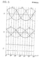
- Fig. 5 shows waveforms obtained when the ripple of the torque waveform is suppressed by modulating the sum of the currents supplied to the three-phase armature coils of the motor with the modulating signal i.
- A shows waveforms of the voltages e 1 , e 2 , e 3 induced in the three-phase coils 4, 5, 6, respectively;
- B shows waveforms of the currents i l , i 2 , i3 supplied to the coils 4, 5, 6 when the sum of the currents flowing into the coils is modulated with the modulating signal i c ;
- C shows a waveform of the torque produced by the motor when the currents shown in B are supplied to the armature coils of the motor.
- the main component of the torque ripple is the twelfth order component.
- the magnitude of the ripple is suppressed to 2.8% p-p .
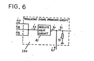
- Fig. 6 shows another example of the modulating signal producing circuit 120.
- the modulating signal i c is produced by taking the difference between the output current i T of the instruction signal producing circuit 80 and the output current i r of the absolute value circuit 61.
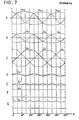
- Fig. 7 shows waveforms appearing at specified portions in the circuit shown in Fig. 1 when the modulating signal producing circuit shown in Fig. 6 is used. Since the waveforms shown in A, B and C in Fig. 7 are the same as the waveforms shown in A, B and C in Fig. 3, they will not be explained herein.
- D shows a waveform of the current is obtained by summing up the output currents i H1 , i H2 , i H3 of the buffer amplifiers 21, 22, 23. The currents i H1 , i H2 , i H3 are shifted in phase by 120° from each other. Each of these current waveforms contains harmonics of the third, fifth and seventh orders.
- the third, fifth and seventh order components account for 12.8%, 4.6%, 1.5%,.respectively, of the fundamental wave.
- the fundamentals and the harmonics of the fifth and seventh orders of the currents i H1 , i H2 , i H3 are canceled out by the addition of these three currents.
- the third order harmonic component is left in the resultant current i s and the magnitude thereof accounts for 38.4% (12.8% x 3) of the fundamental of each of the output currents i H1 , i H2 , i H3 of the buffer circuits 21, 22, 23.
- E shows a waveform of the output current i of the absolute value circuit 61.
- the direction in which the current flows into the circuit 61 is taken as positive direction.
- the relation between the current i and the r total current i is as follows:
- F shows the output current i T of the instruction signal producing circuit 80, the magnitude of the current i T being proportional to the externally given instruction signal E T .
- G shows the current i c flowing into the resistor 71.
- the current i c contains the sixth order ripple component.
- the output current i r (E in Fig. 7) of the circuit 61 is in phase with the ripple component of the torque waveform (C in Fig. 4). Therefore, in order to reverse the phase, the current i r is subtracted from the constant current i T (F in Fig. 7) proportional to the instruction signal.
- the modulating signal i c (G in Fig. 7) is produced.
- the current detecting resistor 90 converts the sum of the currents supplied to the armature coils of the motor into a voltage which is applied to one input terminal of the second error amplifier 70.
- the difference between the output current i T of the instruction-signal producing circuit 80 and the output current irof the absolute value circuit 61 is produced to obtain the modulating signal current i c .
- the current i is converted into a voltage by the resistor 71, and this voltage is applied to the other input terminal of the second error amplifier 70.
- the gains of the power supply circuits 101, 102, 103 are so adjusted that the two input voltages applied to the error amplifier 70 become equal to each other.
- the ripple rate of the modulating signal i c is made equal to that of the ripple waveform shown in C in Fig. 4 to suppress the torque ripple.
- the ripple rate of the modulating signal i c can be arbitrarily set by the resistance ratio of the resistor 82 to the resistor 44. In this case, the resistance of the resistor 82 is set 0.6 times the resistance of the resistor 44 to minimize the torque ripple.
- Fig. 8 shows waveforms obtained when the ripple of the torque waveform is suppressed by modulating the sum of the currents flowing into the armature coils of the motor with the modulating signal i c by the circuit shown in Fig. 1.
- A shows waveforms of the voltages e l , e 2 , e 3 induced in the coils 4, 5, 6;
- B shows waveforms of the currents i l , i 2' i 3 supplied to the coils 4, 5, 6 when the sum of these currents is modulated with the modulating signal i c ;
- C shows a waveform of the torque produced by the motor when the currents shown in B are supplied to the armature coils of the motor.
- the main component of the torque ripple is the twelfth order harmonic.
- the magnitude of the torque ripple is suppressed to 4.2% p-p .
- the main ripple component is the sixth order harmonic and its magnitude is approximately 14% p-p .
- the sixth order harmonic component is reduced below 0.5% p-p . Since the twelfth order harmonic component of the remaining torque ripple has a high frequency, the variation of the rotation of the motor due to the torque ripple is sufficiently attenuated due to the inertia of the rotor. Thus, no practical problems arise.
- the output signal of the first error amplifier 50 controls the gains of the buffer amplifiers 21, 22, 23. But, it is also possible to directly control the input voltages applied to the Hall effect devices 1, 2, 3 by the output signal of the first error amplifier 50.
- Motors to which the novel driving circuit of the invention is applicable are not limited to the flat-type slotless motors as shown in Fig. 2. 'But, the driving circuit of the invention may be applied also to slotted motors and cylindrical motors.
- Hall effect devices are used as the position detectors, but obviously, any other kinds of sensors may also be used as long as they can produce a similar signal as the Hall effect devices.
Abstract
Description
- The present invention relates to a driving circuit for driving brushless DC motors.
- In recent years, brushless DC motors which have their excited armature phases switched in turn by semi-conductor devices (such as transistors) according to signals from rotor position detectors (such as Hall effect devices) have been used in audio and video equipment. Usually, a brushless DC motor needs one rotor position detector and one armature excitation control circuit for exciting each phase. Accordingly, as the number of the phases of the motor increases, complexity of the control circuits increases. This would make the motor expensive and bulky. Hence, this scheme is not put into practical use. Therefore, in general, armatures of two or three phases are adopted. This has normally resulted in torque ripples ranging from 15 to 20%p-p, increasing variations in the motor speed. As a result, the wow or flutter of the audio or video equipment using such a motor increases.
- Brushless DC motors recently available frequently make use of Hall effect devices as rotor position detectors. As is well known, Hall effect devices widely vary in sensitivity. For this reason, various circuit techniques have been employed to accommodate such sensitivity variations. Further, many attempts have been made to reduce torque ripples of brushless DC motors.
- Japanese Laid-Open Patent Application No. 59-35585 (hereinafter referred to as "
reference 1") discloses a typical technique that uses three Hall effect devices as rotor position detectors. The scheme of the driving circuit disclosed inreference 1 is not described in detail herein, but, the operation of the driving circuit is characterized in that the coils are switched at such timings that the signals from the Hall effect devices become zero so as to be less affected by the sensitivity variations among the devices. Further, the operation is characterized in that the electric currents supplied to the coils are partially modulated in response to a signal synchronized with the rotation of the motor for canceling out the torque ripples. - The driving apparatus disclosed in the
aforementioned reference 1 operates based on the timings at which the signals from the Hall effect devices become zero. This offers the advantage that the driving circuit is insusceptible to the sensitivity variations among the Hall effect devices. However, since the armature coils are alternately energized and deenergized, filter circuits containing relatively large capacitors for reducing the spike-like voltage produced by the switching of the coils need to be provided at the power supply terminals to the coils. Also, the driving circuit has the disadvantage that it is likely to produce vibration and noise, because the electric currents flowing into the coils are suddenly caused to cease and commence. - It is an object of the present invention to provide a driving circuit for brushless DC motors which is hardly affected by sensitivity variations among rotor position detector devices and by offset of the detector devices, and produces low vibration, low noise, and low torque ripples.
- In order to achieve this object, a driving circuit for a brushless DC motor according to the present invention comprises: a magnetic pole position detecting circuit for detecting positions of magnetic poles of a rotor magnet of the motor and delivering polyphase signals indicative of the positions; a rectifier adder circuit for producing a sum of positive or negative portions of the polyphase signals from the magnetic pole position detecting circuit; an instruction signal producing circuit for producing a torque instruction signal instructing a torque to be produced by the motor; a first error amplifier for adjusting a gain of the magnetic pole position detecting circuit to make an output signal of the rectifier adder circuit to be proportional to the torque instruction signal; a power supply circuit responsive to the polyphase signals for supplying currents to polyphase armature coils; current detecting means for detecting the currents supplied to the armature coils; a modulating signal producing circuit for modulating the currents supplied to the armature coils; and a second error amplifier for adjusting a gain of the power supply circuit to make an output signal of the current detecting means equal to an output signal of the modulating signal producing circuit.
- The magnetic pole position detecting circuit may comprises rotor position detector devices, buffer amplifiers and subtractors. Output signals from the detector devices are amplified by the buffer amplifiers, and difference signals between two of output signals of the buffer amplifiers X are produced by the subtractor circuits. The rectifier adder circuit produces the sum of positive or negative portions of the difference signals from the subtractor circuits. The output signal of the rectifier adder circuit is controlled to be a constant value proportional to the torque instruction signal. The torque instruction signal may be an externally given signal. As a result, even if the detector devices vary in sensitivity or in offset, torque ripples are hardly produced. Therefore, it is not necessary to take measures either to accommodate sensitivity variations among the detector devices or to adjust their offset.
- The electric currents supplied to polyphase armature coils are converted into a voltage which is so controlled as to coincide with a modulating signal synchronized with the rotation of the motor. More specifically, the currents supplied to the armature coils are so modulated as to have a phase reversed from that of the torque ripples remaining in the motor. This can cancel low-order components of the torque ripples, whereby a circuit for driving a brushless DC motor showing little torque ripples can be obtained.
- The position signals from the position detecting circuit are amplified by the power supply circuit and then supplied to the polyphase armature coils. Therefore, each of the supplied current signals has a sinusoidal waveform. Thus, energization of the coils is not controlled by sudden switching action. Hence, no spike-like voltage (which would normally be caused by switching of electric current) is generated. This can dispense with a filter circuit which has a relatively large capacitor for reducing such spike-like voltage.
- The above and other features and advantages of the invention will be apparent from consideration of the following description taken in conjunction with the accompanying drawings in which:
- Fig. 1 is a circuit diagram showing an embodiment of driving circuit according to the invention;
- Fig. 2 is a perspective view of a main portion of a motor to which the invention is preferable applied;
- Fig. 3 is a diagram showing waveforms appearing at specified portions in the driving circuit shown in Fig. 1;
- Fig. 4 is a waveform diagram obtained when the sum of the electric currents supplied to three-phase armature coils is not modulated;
- Fig. 5 is a waveform diagram obtained when the sum of the electric currents supplied to three-phase armature coils is modulated;
- Fig. 6 is a circuit diagram of another example of modulating signal producing circuit that can be used in the driving circuit shown in Fig. 1;
- Fig. 7 is a diagram showing waveforms appearing at specified portions in the driving circuit shown in Fig. 1 when the driving circuit uses the modulating signal producing circuit shown in Fig. 6; and
- Fig. 8 is a waveform diagram obtained when the sum of the electric currents supplied to three-phase armature coils is modulated with the output signal from the modulating signal producing circuit shown in Fig. 6.
- Fig. 2 is a perspective view of a main portion of an electric motor to which the invention is preferably applied. This motor has a rotating
shaft 7 mounting thereon adisk 8 made of soft iron which serves as a back yoke. A disklike rotor magnet 9 is rigidly fixed to the bottom surface of thedisk 8 to constitute a rotor. - Three-
phase armature coils stator 10 made of a soft iron plate. Theshaft 7 is rotatably held by abearing 11 that is secured to thestator 10 at a position surrounded by thecoils Hall effect devices 1, 2, 3 are disposed at the centers of thecoils - Fig. 1 is a circuit diagram showing an example of driving circuit according to the invention. The driving circuit has a magnetic pole
position detecting circuit 110 that detects positions of magnetic poles of the rotor magnet 9 and delivers three-phase signals indicating the positions. The detectingcircuit 110 has aDC power supply 20 for supplying a voltage to the threeHall effect devices 1, 2, 3.Buffer amplifiers Hall effect devices 1, 2, 3, respectively. In this example, the amplifiers 21-23 respectively convert differential output signals from the Hall effect devices 1-3 into currents iH1, iH2, iH3, which are proportional to the differential output signals. Each of the amplifiers 21-23 delivers three output currents of same magnitude. - The detecting
circuit 110 further includessubtractor circuits buffer amplifier 21 and the output current iS2 of thebuffer amplifier 22 are applied to thesubtractor circuit 31 which produces a difference signal between them,.i.e., a current iP1 (= i Hl - iH2). The output current iH2 of thebuffer amplifier 22 and the output current iH3 of thebuffer amplifier 23 are supplied to thesubtractor circuit 32 which produces a difference signal between them, i.e., a current iP2 (= iH2 - iH3). Similarly, the output current iH3 of thebuffer amplifier 23 and the output current iH1 of thebuffer amplifier 21 are supplied to thesubtractor circuit 33 which produces a difference signal between them, i.e., a current ip3 (=iH3 - iH1). Each of thesubtractor circuits subtractor circuits power supply circuits subtractor circuits rectifier adder circuit 40 consisting of diodes 41, 42, 43 and aresistor 44. Thecircuit 40 allows only the positive portions of the output currents iP1, ip2, ip3 of thesubtractor circuits resistor 44 to thereby produce a voltage corresponding to a sum of the rectified currents. - An instruction signal producing circuit 80 has two output terminals at each of which an electric current (torque instruction signal) iT proportional to a signal ET instructing a torque appears. One output current iT is applied to a
resistor 82 so as to be converted into a voltage which is applied to one input terminal of afirst error amplifier 50. The other input terminal of theamplifier 50 receives the sum of the rectified currents from therectifier adder circuit 40. Thefirst error amplifier 50 adjusts gains of the amplifiers 21-23 in such a way that the two input voltages applied thereto become equal to each other. - A modulating
signal producing circuit 120 receives the currents iH1, iH2, iH3 from thebuffer amplifiers circuit 120 is composed of an absolutevalue adder circuit 60 for converting the currents iH1, iH2' iH3 into absolute values and summing up them, and a combining circuit for delivering the modulating signal ic which is a difference between the instruction signal iT from the circuit 80 and an output current i from theadder circuit 60. - The three-
phase armature coils power supply circuits DC power supply 114.Resistors subtractor circuits - A resistor (Rcs) 90 is used to detect the currents i1, i2' i3 supplied to the
coils second error amplifier 70 has two input terminals to one of which a voltage detected by theresistor 90 is applied. The modulating signal produced by the modulatingsignal producing circuit 120 is applied to the other input terminal. In this example, the output current ir from the absolutevalue adder circuit 60 is subtracted from the output current iT from the instruction signal producing circuit 80 to yield the difference current ic (= iT - ir) which is converted into a voltage by means of a resistor 71. This voltage is applied to the other input terminal of thesecond error amplifier 70 as the modulating signal. Thesecond error amplifier 70 adjusts gains of the threepower supply circuits second error amplifier 70 become equal to each other. The operation of the driving circuit for a brushless DC motor constructed as described above will next be described with reference to Figs. 3, 4, 5. - Fig. 3
shows rotating angle 6 of the rotor in terms of electrical angle and waveforms appearing at specified portions in the driving circuit shown in Fig. 1. In Fig. 3, A shows waveforms of the differential output voltages eH1, eH2, eH3 from theHall effect devices 1, 2, 3. The voltage eH1 becomes positive at a point where 6 = 0°. The voltage eH2 lags relative to the voltage eH1 by 120°. Also, the voltage eH3 lags relative to the voltage eH2 by 120°. It is assumed that theHall effect devices 1, 2, 3 do not differ in sensitivity and that they show no offset. - In general, motors of permanent magnet rotor type have their permanent magnets magnetized in the form of trapezoidal wave in order to enhance the efficiency and productivity of the motors. Therefore, the differential output voltages from the Hall effect devices acting to detect the magnetic field contain harmonic components up to higher orders. In the example shown in A, components of the third, fifth and seventh orders account for 12.6%, 2.5% and 0.6%, respectively, of the fundamental wave.
- In Fig. 3, B shows waveforms of the output currents iH1, iH2, iH3 of the
buffer amplifiers subtractor circuits - Since the
buffer amplifiers subtractor circuits rectifier adder circuit 40, and thefirst error amplifier 50 constitute a control loop, the peak values of the output currents iP1, iP2, iP3 of thesubtractor circuits subtractor circuits - In Fig. 3, D shows a waveform of the output current ir of the absolute
value adder circuit 60. Here, the direction in which current flows into thecircuit 60 is taken as positive direction. The output current ir of the absolutevalue adder circuit 60 is expressed as:
circuit 60 is given by i = iT - ir. The waveform of the current ic contains ripples of the sixth order. - Referring again to Fig. 1, as mentioned already, the
power supply circuits resistor 90 for converting the electric currents flowing into the armature coils 4, 5, 6 into voltages, and thesecond error amplifier 70 constitute the control loop. Thesecond error amplifier 70 is applied with the voltage developed by theresistor 90 and the voltage produced by the resistor 71, and adjusts the gains of the power supply circuits 101-103. The operation of the control loop will next be described by referring to Figs. 4 and 5. - Fig. 4 shows waveforms when the output terminal of the absolute
value adder circuit 60 is open-circuited. In Fig. 4, A shows waveforms of the three-phase voltages el, e2, e3 which are induced in the three-phase armature coils coils - In Fig. 4, B shows the currents i1, i2, i3 supplied to the armature coils 4, 5, 6, respectively. The output currents iP1, iP2, iP3 of the
subtractor circuits power supply circuits value adder circuit 60 is disabled, the gains of thepower supply circuits coils subtractor circuits subtractor circuits buffer amplifiers 
coils power supply circuits - In Fig. 4, C shows a waveform of the torque produced by the motor when the armature coils of the motor are excited with the currents shown in B. The torque produced by the motor is proportional to a sum of products of the voltages el, e2, e3 (shown in A) induced in the coils and the currents i1, i2, i3 (shown in B) supplied to the coils. That is, the torque is proportional to (ei·i1 + e2·i2 + e3·i3). As shown in Fig. 4, the maximum value of the produced torque appears at 6 = 30°, 90°, 150°, 210°, ..., and the minimum value appears at θ = 0°, 60°, 120°, 180°, .... The main component of the.torque ripple is the sixth order component.
- In the present example, when the output terminal of the absolute
value adder circuit 60 is open-circuited, i.e., when the gains of thepower supply circuits - In order to suppress this torque ripple, the gains are not controlled to keep constant the sum of the currents flowing into the coils, but rather the gains may be controlled so that the sum of the currents is so modulated as at to be the same in ripple rate as and reversed in phase from the torque waveform C shown in Fig. 4.
- In the circuit shown in Fig. 1 for driving the brushless DC motor, the modulating signal is produced by the absolute
value adder circuit 60 to suppress the torque ripple shown in Fig. 4. The output current i (D in Fig. 3) of thecircuit 60 is in phase with the torque ripple contained in the torque waveform (C in Fig. 4). To reverse the phase, the current ir is subtracted from the constant current iT (E in Fig. 3) proportional to the instruction signal to produce the modulating signal ic (F in Fig. 3). The voltage developed across the current detectingresistor 90 converts the sum of the currents flowing into the coils to a voltage which is applied to one input terminal of thesecond error amplifier 70. The other input terminal of theamplifier 70 receives a voltage obtained by converting the modulating signal ic by the use of the resistor 71. The modulating signal ic is the difference between the output current iT of the instruction signal producing circuit 80 and the output current i of the absolutevalue adder circuit 60. The r gains of thepower supply circuits second error amplifier 70 become equal to each other. The ripple rate of the modulating signal ic is made equal to that of the torque waveform (C in Fig. 4) to suppress the torque ripple. - The ripple rate of the modulating signal i can be arbitrarily set by the resistance ratio of the
resistor 82 to theresistor 44. In this example, the resistance of theresistor 82 is set 0.35 times that of theresistor 44 to minimize the torque ripple. In any case that the harmonics contents of the waveforms of the differential output voltages of the Hall effect devices and of the waveforms of the voltages induced in the coils differ from those in the above case, the resistance ratio of theresistor 44 to theresistor 82 may be changed to an appropriate value to minimize the torque ripple. - This setting of the resistance ratio needs not be performed for each individual motor of the same structure, because the harmonics contents of the differential output voltages of the Hall effect devices and of the voltages induced in the coils are considered substantially the same for all motors of the same structure.
- Fig. 5 shows waveforms obtained when the ripple of the torque waveform is suppressed by modulating the sum of the currents supplied to the three-phase armature coils of the motor with the modulating signal i. In Fig. 5, A shows waveforms of the voltages e1, e2, e3 induced in the three-
phase coils coils - Fig. 6 shows another example of the modulating
signal producing circuit 120. This circuit consists of anabsolute value circuit 61 to which a sum i of the output currents iH1, iH2, i H3 of thebuffer amplifiers absolute value circuit 61. - Fig. 7 shows waveforms appearing at specified portions in the circuit shown in Fig. 1 when the modulating signal producing circuit shown in Fig. 6 is used. Since the waveforms shown in A, B and C in Fig. 7 are the same as the waveforms shown in A, B and C in Fig. 3, they will not be explained herein. In Fig. 7, D shows a waveform of the current is obtained by summing up the output currents iH1, iH2, i H3 of the
buffer amplifiers buffer circuits - In Fig. 7, E shows a waveform of the output current i of the
absolute value circuit 61. The direction in which the current flows into thecircuit 61 is taken as positive direction. The relation between the current i and the r total current i is as follows:
- In Fig. 7, F shows the output current iT of the instruction signal producing circuit 80, the magnitude of the current iT being proportional to the externally given instruction signal ET.
- In Fig. 7, G shows the current ic flowing into the resistor 71. There exists the relation ic = iT - ir between the output current iT of the instruction signal producing circuit 80 and the output current ir of the
absolute value circuit 61. The current i c (G in Fig. 7) contains the sixth order ripple component. As shown in Fig. 7, the output current ir (E in Fig. 7) of thecircuit 61 is in phase with the ripple component of the torque waveform (C in Fig. 4). Therefore, in order to reverse the phase, the current ir is subtracted from the constant current iT (F in Fig. 7) proportional to the instruction signal. Thus, the modulating signal i c (G in Fig. 7) is produced. The current detectingresistor 90 converts the sum of the currents supplied to the armature coils of the motor into a voltage which is applied to one input terminal of thesecond error amplifier 70. The difference between the output current iT of the instruction-signal producing circuit 80 and the output current irof theabsolute value circuit 61 is produced to obtain the modulating signal current ic. The current i is converted into a voltage by the resistor 71, and this voltage is applied to the other input terminal of thesecond error amplifier 70. The gains of thepower supply circuits error amplifier 70 become equal to each other. The ripple rate of the modulating signal ic is made equal to that of the ripple waveform shown in C in Fig. 4 to suppress the torque ripple. The ripple rate of the modulating signal ic can be arbitrarily set by the resistance ratio of theresistor 82 to theresistor 44. In this case, the resistance of theresistor 82 is set 0.6 times the resistance of theresistor 44 to minimize the torque ripple. - Fig. 8 shows waveforms obtained when the ripple of the torque waveform is suppressed by modulating the sum of the currents flowing into the armature coils of the motor with the modulating signal ic by the circuit shown in Fig. 1. In Fig. 8, A shows waveforms of the voltages el, e2, e3 induced in the
coils coils - As already described in connection with Fig. 4, when the sum of the currents flowing into the
coils coils - In the example described in conjunction with Fig. 1, the output signal of the
first error amplifier 50 controls the gains of thebuffer amplifiers Hall effect devices 1, 2, 3 by the output signal of thefirst error amplifier 50. - Motors to which the novel driving circuit of the invention is applicable are not limited to the flat-type slotless motors as shown in Fig. 2. 'But, the driving circuit of the invention may be applied also to slotted motors and cylindrical motors. In the description above, Hall effect devices are used as the position detectors, but obviously, any other kinds of sensors may also be used as long as they can produce a similar signal as the Hall effect devices.
Claims (8)
buffer amplifiers (21,22,23) for amplifying output signals of the magnetoelectric converter devices (1,2,3).
Applications Claiming Priority (4)
| Application Number | Priority Date | Filing Date | Title |
|---|---|---|---|
| JP59277169A JPS61150695A (en) | 1984-12-25 | 1984-12-25 | Drive device of dc commutatorless motor |
| JP277169/84 | 1984-12-25 | ||
| JP60137255A JPH0716312B2 (en) | 1985-06-24 | 1985-06-24 | DC non-commutator motor drive |
| JP137255/85 | 1985-06-24 |
Publications (2)
| Publication Number | Publication Date |
|---|---|
| EP0189676A1 true EP0189676A1 (en) | 1986-08-06 |
| EP0189676B1 EP0189676B1 (en) | 1990-02-28 |
Family
ID=26470630
Family Applications (1)
| Application Number | Title | Priority Date | Filing Date |
|---|---|---|---|
| EP85309487A Expired - Lifetime EP0189676B1 (en) | 1984-12-25 | 1985-12-24 | Driving circuit for brushless dc motors |
Country Status (5)
| Country | Link |
|---|---|
| US (1) | US4633150A (en) |
| EP (1) | EP0189676B1 (en) |
| KR (1) | KR900005813B1 (en) |
| CN (1) | CN1004040B (en) |
| DE (1) | DE3576254D1 (en) |
Cited By (2)
| Publication number | Priority date | Publication date | Assignee | Title |
|---|---|---|---|---|
| DE3610253A1 (en) * | 1986-03-26 | 1987-10-08 | Sgs Halbleiterbauelemente Gmbh | CONTROL CIRCUIT FOR A COMMUTATORLESS DC MOTOR |
| EP0765026A1 (en) * | 1995-09-20 | 1997-03-26 | Matsushita Electric Industrial Co., Ltd. | Brushless motor |
Families Citing this family (38)
| Publication number | Priority date | Publication date | Assignee | Title |
|---|---|---|---|---|
| US4763347A (en) * | 1983-02-02 | 1988-08-09 | General Electric Company | Control system, electronically commutated motor system, blower apparatus and methods |
| US5023527A (en) | 1974-06-24 | 1991-06-11 | General Electric Company | Control circuits, electronically commutated motor systems and methods |
| DE3537403C2 (en) * | 1985-10-21 | 1995-06-01 | Papst Motoren Gmbh & Co Kg | Brushless DC motor with or for a fan |
| US4902944A (en) * | 1986-11-20 | 1990-02-20 | Staubli International Ag. | Digital robot control having an improved current sensing system for power amplifiers in a digital robot control |
| JPH0750880Y2 (en) * | 1988-09-29 | 1995-11-15 | 株式会社三協精機製作所 | Brushless motor drive circuit |
| KR930007174B1 (en) * | 1989-03-31 | 1993-07-31 | 가부시기가이샤 도시바 | Pick-up transferring device |
| JP2554374B2 (en) * | 1989-07-03 | 1996-11-13 | 株式会社三協精機製作所 | Brushless motor drive circuit |
| JPH03135392A (en) * | 1989-10-19 | 1991-06-10 | Sankyo Seiki Mfg Co Ltd | Circuit for driving brushless motor |
| DE4040926C1 (en) * | 1990-12-20 | 1992-04-16 | Robert Bosch Gmbh, 7000 Stuttgart, De | |
| JP2624382B2 (en) * | 1991-01-21 | 1997-06-25 | 株式会社三協精機製作所 | Drive circuit for brushless motor |
| JP2750788B2 (en) * | 1991-08-08 | 1998-05-13 | ローム株式会社 | Motor control circuit and motor control device |
| US5191269A (en) * | 1991-10-10 | 1993-03-02 | Sgs-Thomson Microelectronics, Inc. | Brushless direct current motor with minimized current ripple and method |
| US5319289A (en) * | 1992-02-24 | 1994-06-07 | Silicon Systems, Inc. | Adaptive commutation delay for multi-pole brushless DC motors |
| US5668449A (en) * | 1994-10-27 | 1997-09-16 | Sgs-Thomson Microelectronics, Inc. | Motor with input-controlled high side driver |
| US5614797A (en) * | 1995-02-28 | 1997-03-25 | Sgs-Thomson Microelectronics, Inc. | Stator coil driver circuit for a brushless DC motor |
| US5731670A (en) * | 1995-03-31 | 1998-03-24 | Sgs-Thomson Microelectronics S.R.L. | Method for driving a brushless DC electric motor |
| GB9600549D0 (en) * | 1996-01-11 | 1996-03-13 | Lucas Ind Plc | Motor drive control |
| JPH09271192A (en) * | 1996-03-29 | 1997-10-14 | Sharp Corp | Driving equipment of brushless motor |
| US5969489A (en) * | 1996-07-31 | 1999-10-19 | Victor Company Of Japan, Ltd. | Motor driving system for driving brushless motor |
| US5869946A (en) * | 1997-02-27 | 1999-02-09 | Stmicroelectronics, Inc. | PWM control of motor driver |
| US5952817A (en) * | 1997-04-24 | 1999-09-14 | Linear Technology Corporation | Apparatus and method using waveform shaping for reducing high frequency noise from switching inductive loads |
| US6130989A (en) * | 1998-07-17 | 2000-10-10 | Sanyo Electric Co., Ltd. | Motor drive circuit |
| TW453018B (en) * | 1998-07-31 | 2001-09-01 | Sanyo Electric Co | Motor driving circuit |
| EP0989552B1 (en) | 1998-09-02 | 2005-10-26 | Matsushita Electric Industrial Co., Ltd. | Disk drive apparatus and motor |
| US6046555A (en) * | 1998-10-23 | 2000-04-04 | Nippon Kogaku Kk | System and method for determining a magnetic offset of a brushless DC motor |
| US6710567B2 (en) | 2000-11-27 | 2004-03-23 | Seagate Technology Llc | Velocity dependent reference profile for spindle motor acceleration control |
| US6577088B2 (en) | 2001-02-09 | 2003-06-10 | Seagate Technology Llc | Closed loop spindle motor acceleration control in a disc drive |
| US6664749B2 (en) | 2001-04-06 | 2003-12-16 | Seagate Technology Llc | Spindle motor initialization after a control processor reset condition in a disc drive |
| US6940235B2 (en) * | 2001-05-10 | 2005-09-06 | Analog Devices, Inc. | Method and apparatus for driving a brushless DC motor |
| US6744587B2 (en) | 2001-06-29 | 2004-06-01 | Seagate Technology Llc | Motor control circuit with adaptive controller path selection for different load conditions |
| US6707269B2 (en) | 2001-09-11 | 2004-03-16 | Seagate Technology Llc | Motor control circuit with adaptive dynamic range selection |
| US7012391B2 (en) * | 2002-08-09 | 2006-03-14 | Seagate Technology Llc | Motor acceleration using continuous sequence of current limit values |
| US6741049B2 (en) * | 2002-10-28 | 2004-05-25 | Melexis Nv Miroelectronics Integrated Systems | Low voltage start up circuit for brushless DC motors |
| US7404073B2 (en) | 2003-06-26 | 2008-07-22 | Seagate Technology Llc | Transitioning from startup code to application code during initialization of a processor based device |
| US6859001B2 (en) * | 2003-07-24 | 2005-02-22 | General Electric Company | Torque ripple and noise reduction by avoiding mechanical resonance for a brushless DC machine |
| JP4221307B2 (en) * | 2004-01-07 | 2009-02-12 | 日立アプライアンス株式会社 | Synchronous motor control device, electrical equipment and module |
| JP2008301678A (en) * | 2007-06-04 | 2008-12-11 | Ntn Corp | Drive control circuit of polyphase motor, and spindle device using this |
| CN114151936A (en) * | 2020-09-07 | 2022-03-08 | 中山大洋电机股份有限公司 | HVAC system control unit and HVAC system |
Family Cites Families (6)
| Publication number | Priority date | Publication date | Assignee | Title |
|---|---|---|---|---|
| JPS5364711A (en) * | 1976-11-19 | 1978-06-09 | Sony Corp | Brushless motor drive circuit |
| JPS5749386A (en) * | 1980-09-10 | 1982-03-23 | Hitachi Ltd | Rotary phase detector for rotor |
| JPS58139687A (en) * | 1982-02-10 | 1983-08-19 | Mitsubishi Electric Corp | Controller for transistor motor |
| JPH0632586B2 (en) * | 1983-04-20 | 1994-04-27 | ソニー株式会社 | 3-phase DC motor |
| JPS59194694A (en) * | 1983-04-20 | 1984-11-05 | Sony Corp | Drive circuit of 3-phase bidirectional energization brushless motor |
| JPS59198891A (en) * | 1983-04-22 | 1984-11-10 | Hitachi Ltd | Drive circuit of motor |
-
1985
- 1985-12-03 US US06/804,259 patent/US4633150A/en not_active Expired - Fee Related
- 1985-12-18 KR KR1019850009544A patent/KR900005813B1/en not_active IP Right Cessation
- 1985-12-24 DE DE8585309487T patent/DE3576254D1/en not_active Expired - Lifetime
- 1985-12-24 EP EP85309487A patent/EP0189676B1/en not_active Expired - Lifetime
- 1985-12-25 CN CN85109333.7A patent/CN1004040B/en not_active Expired
Non-Patent Citations (3)
| Title |
|---|
| PATENT ABSTRACTS OF JAPAN, vol. 7, no. 103 (E-173)[1248], 6th May 1983; & JP - A - 58 26583 (SEKOH GIKEN K.K.) 17-02-1983 * |
| PATENT ABSTRACTS OF JAPAN, vol. 8, no. 123 (E-249)[1560], 8th June 1984; & JP - A - 59 35585 (MATSUSHITA DENKI SANGYO K.K.) 27-02-1984 * |
| PATENT ABSTRACTS OF JAPAN, vol. 8, no. 36 (E-227)[1473], 16th February 1984; & JP - A - 58 192 490 (MATSUSHITA DENKI SANGYO K.K.) 09-11-1983 * |
Cited By (5)
| Publication number | Priority date | Publication date | Assignee | Title |
|---|---|---|---|---|
| DE3610253A1 (en) * | 1986-03-26 | 1987-10-08 | Sgs Halbleiterbauelemente Gmbh | CONTROL CIRCUIT FOR A COMMUTATORLESS DC MOTOR |
| US4814674A (en) * | 1986-03-26 | 1989-03-21 | Sgs Halbleiter-Bauelemente Gmbh | Control circuit for a brushless DC motor |
| EP0765026A1 (en) * | 1995-09-20 | 1997-03-26 | Matsushita Electric Industrial Co., Ltd. | Brushless motor |
| US5767640A (en) * | 1995-09-20 | 1998-06-16 | Matsushita Electric Industrial Co., Ltd. | Brushless motor |
| US5969490A (en) * | 1995-09-20 | 1999-10-19 | Matsushita Electric Industrial Co., Ltd. | Brushless motor for providing precise driving signal in presence of variations in output amplitude of position detecting signal |
Also Published As
| Publication number | Publication date |
|---|---|
| DE3576254D1 (en) | 1990-04-05 |
| KR860005478A (en) | 1986-07-23 |
| US4633150A (en) | 1986-12-30 |
| CN1004040B (en) | 1989-04-26 |
| KR900005813B1 (en) | 1990-08-11 |
| EP0189676B1 (en) | 1990-02-28 |
| CN85109333A (en) | 1986-07-09 |
Similar Documents
| Publication | Publication Date | Title |
|---|---|---|
| EP0189676B1 (en) | Driving circuit for brushless dc motors | |
| US4658190A (en) | Reduced ripple drive circuit for a brushless motor | |
| US4651067A (en) | Apparatus for driving brushless motor | |
| US6498449B1 (en) | Low ripple torque control of a permanent magnet motor without using current sensors | |
| US4255693A (en) | Closed loop stepper motor circuitry without encoder | |
| JP3000453B2 (en) | Commutatorless DC motor and generator | |
| US6693407B2 (en) | Controller and associated system and method for pulse-width-modulation switching noise reduction by voltage control | |
| US5444355A (en) | Charging generator for a vehicle | |
| JP2741214B2 (en) | Brushless D. C motor | |
| JPH08172764A (en) | Brushless motor | |
| KR930022699A (en) | Non-commutator DC Motor | |
| US4008425A (en) | Motor servo system with multiplier means to drive and servo the motor | |
| JP2001500357A (en) | Angular position detector for synchronous motor control excited by permanent magnet | |
| GB1440089A (en) | Speed control of brushless dc motors | |
| JPH0345634B2 (en) | ||
| US4131828A (en) | Apparatus for rotatively driving a turn table | |
| US3242405A (en) | Brushless electric motor | |
| US5130590A (en) | Brushless generator regulated by second rotor | |
| KR900001792B1 (en) | Control method and apparatus for synchronous motor | |
| JPH0378491A (en) | Drive equipped with driving motor | |
| JPH09331695A (en) | Rotor position detection for synchronous motor and device therefor | |
| EP0154863B1 (en) | Apparatus for driving polyphase brushless motor | |
| US5485071A (en) | Method and apparatus for establishing a reference current for use in operating a synchronous motor | |
| JPS6333395B2 (en) | ||
| US3195032A (en) | Stabilizing system for synchronous motor or generator |
Legal Events
| Date | Code | Title | Description |
|---|---|---|---|
| PUAI | Public reference made under article 153(3) epc to a published international application that has entered the european phase |
Free format text: ORIGINAL CODE: 0009012 |
|
| AK | Designated contracting states |
Kind code of ref document: A1 Designated state(s): DE FR GB |
|
| 17P | Request for examination filed |
Effective date: 19870102 |
|
| 17Q | First examination report despatched |
Effective date: 19890410 |
|
| GRAA | (expected) grant |
Free format text: ORIGINAL CODE: 0009210 |
|
| AK | Designated contracting states |
Kind code of ref document: B1 Designated state(s): DE FR GB |
|
| ET | Fr: translation filed | ||
| REF | Corresponds to: |
Ref document number: 3576254 Country of ref document: DE Date of ref document: 19900405 |
|
| PLBE | No opposition filed within time limit |
Free format text: ORIGINAL CODE: 0009261 |
|
| STAA | Information on the status of an ep patent application or granted ep patent |
Free format text: STATUS: NO OPPOSITION FILED WITHIN TIME LIMIT |
|
| 26N | No opposition filed | ||
| PGFP | Annual fee paid to national office [announced via postgrant information from national office to epo] |
Ref country code: FR Payment date: 19961211 Year of fee payment: 12 |
|
| PGFP | Annual fee paid to national office [announced via postgrant information from national office to epo] |
Ref country code: GB Payment date: 19961216 Year of fee payment: 12 |
|
| PGFP | Annual fee paid to national office [announced via postgrant information from national office to epo] |
Ref country code: DE Payment date: 19961231 Year of fee payment: 12 |
|
| PG25 | Lapsed in a contracting state [announced via postgrant information from national office to epo] |
Ref country code: GB Free format text: LAPSE BECAUSE OF NON-PAYMENT OF DUE FEES Effective date: 19971224 |
|
| PG25 | Lapsed in a contracting state [announced via postgrant information from national office to epo] |
Ref country code: FR Free format text: THE PATENT HAS BEEN ANNULLED BY A DECISION OF A NATIONAL AUTHORITY Effective date: 19971231 |
|
| GBPC | Gb: european patent ceased through non-payment of renewal fee |
Effective date: 19971224 |
|
| PG25 | Lapsed in a contracting state [announced via postgrant information from national office to epo] |
Ref country code: DE Free format text: LAPSE BECAUSE OF NON-PAYMENT OF DUE FEES Effective date: 19980901 |
|
| REG | Reference to a national code |
Ref country code: FR Ref legal event code: ST |