EP0186382B1 - Programmable digital hysteresis circuit - Google Patents
Programmable digital hysteresis circuit Download PDFInfo
- Publication number
- EP0186382B1 EP0186382B1 EP85309017A EP85309017A EP0186382B1 EP 0186382 B1 EP0186382 B1 EP 0186382B1 EP 85309017 A EP85309017 A EP 85309017A EP 85309017 A EP85309017 A EP 85309017A EP 0186382 B1 EP0186382 B1 EP 0186382B1
- Authority
- EP
- European Patent Office
- Prior art keywords
- digital
- signal
- digital signal
- correction factor
- data store
- Prior art date
- Legal status (The legal status is an assumption and is not a legal conclusion. Google has not performed a legal analysis and makes no representation as to the accuracy of the status listed.)
- Expired - Lifetime
Links
Images


Classifications
-
- G—PHYSICS
- G01—MEASURING; TESTING
- G01R—MEASURING ELECTRIC VARIABLES; MEASURING MAGNETIC VARIABLES
- G01R13/00—Arrangements for displaying electric variables or waveforms
- G01R13/02—Arrangements for displaying electric variables or waveforms for displaying measured electric variables in digital form
-
- H—ELECTRICITY
- H03—ELECTRONIC CIRCUITRY
- H03M—CODING; DECODING; CODE CONVERSION IN GENERAL
- H03M1/00—Analogue/digital conversion; Digital/analogue conversion
- H03M1/06—Continuously compensating for, or preventing, undesired influence of physical parameters
- H03M1/08—Continuously compensating for, or preventing, undesired influence of physical parameters of noise
- H03M1/0836—Continuously compensating for, or preventing, undesired influence of physical parameters of noise of phase error, e.g. jitter
Definitions
- This invention relates generally to digitised alpha-numeric displays and more particularly to a means for reducing instability in the readout of a binary digital signal subject to errors from noise, jitter, or threshold uncertainty superposed thereon.
- the present invention may be adapted for use with an on-board aircraft radar antenna system, the overall system including a mechanical drive for redirecting the antenna to a desired position.
- the drive system is controlled by a digital circuit which includes a potentiometer having a control knob located at a control panel in the aircraft cockpit. Rotation of the control knob generates a digital command signal which causes the drive system to rotate the antenna to a position dependent on the amplitude and direction of rotation of the control knob.
- a digital readout indicator located in the cockpit is coupled to receive the digital command signal which reflects the antenna position as the control knob is rotated.
- the sequential progression of numerals on the readout indicator will come to rest at a finite value, thereby indicating the present position of the antenna.
- the progression of numerals on the readout indicator continues to fluctuate, that is move erratically from one number to another, leading to uncertainty as to the actual position of the antenna.
- Noise may be defined as a random or periodic disturbance superposed upon the useful signal tending to obscure the information content of the latter. Such noise may be produced, for example, by thermal agitation in electronic circuit components or by coupling from adjacent circuits, such as switching power supplies and other pulse sources. Jitter refers to the small, rapid aberrations in the indicated signal which are time, amplitude, frequency, or phase related, and which may result, for example, from the wiping action of a movable contact on the control knob. Threshold uncertainty results from the condition where the control knob is left in a transition position such that it is at the threshold of producing a change in digital values, and hence the digital readout does not have a unique input signal.
- High-grade smoothing refers to the use of a filter circuit, which may comprise a network of resistors and capacitors which are coupled to the analogue signal to be processed, thereby removing selectively a broad band of undesired frequency components which contribute to noise and jitter.
- a filter circuit which may comprise a network of resistors and capacitors which are coupled to the analogue signal to be processed, thereby removing selectively a broad band of undesired frequency components which contribute to noise and jitter.
- this technique can result in a noticeable delay between rotation of the control knob and the resultant display due to phase shift in the network, and does not prevent the signal from being adjusted close to a digital threshold which will cause uncertainty.
- dedigitising and positive feedback is a technique in which an analogue signal from the position control is converted to digital form by means of an analogue digital converter for transmission.
- the digitised signal is then reconverted to analogue form by means of a digital/analogue converter.
- a small fraction of the recovered analogue signal is summed with the analogue signal from the position control to provide feedback to the analogue/digital converter.
- a further technique that has been suggested is the elimination of low order bits, which effectively disables the system response to small changes.
- this results in an undesirable loss of sensitivity to the operator, since the readout appears to progress in quantum steps such as 2.0, 2.3, 2.6 etc., rather than the smaller increments with which the control knob may be capable of being adjusted and which the operator will expect to observe.
- US-A-4,224,569 discloses digital control apparatus for stabilising the value of an input digital signal having error components superposed thereon by interposing a predetermined value of hysteresis, the apparatus comprising data output means for generating a reference digital signal for energising a digital display.
- the present invention is characterised by the provision of addressable digital data store means for storing correction factor signals in binary form representative of differences between the input digital signal and the reference digital signal for differences that exceed the predetermined value of hysteresis and for storing a quiescent command representative of no change in the reference digital signal for differences that do not exceed the predetermined value of hysteresis, the correction factor signals being retrievable from the data store means by addressing them by the input digital signal and the reference digital signal, and means (U 5 , U s ) for applying the correction factor signals to the data output means so as to increment or decrement the output means in a direction to reduce differences between the input digital signal and the reference digital signal when the differences exceed the predetermined value of hysteresis and for applying the quiescent command to the data output means so as to effect no change in the reference digital signal when said differences do not exceed the predetermined value of hysteresis.
- the present invention has particular, but not exclusive, application to the stabilisation of the numerical indication of the position of a selectively movable on-board aircraft radar antenna which otherwise provides an erratic output which is not indicative of the true position of the antenna by generating a stable reference digital signal for driving the antenna and the indicator, and varying the reference signal in accordance with predetermined digital values stored in a digital memory comparator, whereby a command signal is generated to correct the reference digital signal in a direction so as to reduce differences between the value of the unstable input signal and the reference digital signal when the differences exceed an error or hysteresis zone corresponding to predetermined values stored in the memory.
- the present invention disclosed overcomes the foregoing problems by providing a digital circuit for converting a binary digital signal encumbered by noise, jitter and threshold uncertainty into a controlled, smoothly varying digital output data signal by applying digital hysteresis to the positional signal.
- the hysteresis values and error correction values are embodied in a programmable addressable memory.
- a digital control apparatus for reducing instability in the readout of a digital input signal by interposing a predetermined value of hysteresis comprises a data output generator in the form of an up-down counter to generate a stable reference digital output signal which is applied to energise the digital display.
- the digital input signal and the reference digital output signal are applied to a digital data store in the form of a programmable read only memory apportioned to respond to groups of high order and lower order bits. Correction factors in -the form of binary words stored in the memory are addressed by the apportioned signals and applied to increment or decrement the up-down counter.
- the counter is thus adjusted to minimise differences in the values of the data input and output signals and bring the value of the reference signal into concurrence with the input binary digital signal, but since the reference signal does not respond to the noise, jitter, and control threshold uncertainty, this tends to smooth and stabilise the output display.
- the hysteresis zone provided by the programmable memory inhibits the system from responding to small deviations in the input binary signal within a predetermined range of values.
- the invention comprises apparatus for providing digital hysteresis to a noisy digital signal for stabilising the output of an alphanumeric display.
- the hysteresis values are stored in a digital memory which is addressed by the input digital signal in binary form and by a reference digital signal.
- the values stored in the memory are representative of predetermined differences in values of the input and reference digital signals.
- the reference signal value is incremented or decremented according to the values addressed to agree with the input signal and is used to energise the alphanumeric display. Changes in the alphanumeric display are inhibited until the difference values exceed a predetermined change, defined as the hysteresis. Thus, perturbations in the digital readout are minimised to values which are not apparent to the operator.
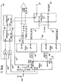
- An input signal 10 which may be an analogue signal derived from a control transducer is applied to an analogue digital-converter U i .
- the converter U 1 forms no part of the present invention and is of a conventional type which samples and digitises an input analogue signal in synchronism with a clock pulse. It is shown here for clarity in illustrating the interface of the invention.
- a clock signal 12 at a frequency of approximately 100 Hz will be applied to converter U 1 which also provides a Data Ready output signal at terminal DR to enable a PROM U 4 when the conversion process has been completed and to signal that the data has settled and is ready for a transfer to the readout circuitry.
- the Data Ready signal is coupled to the PROM U 4 via a line 14 and controlled by the conversion clock at 12.
- the converter U 1 generates an eight-bit data word which is organised into a low order four-bit field and a high order four-bit field, shown coupled to PROMs U 3 and U 2 on buses 16 and 18, respectively.
- Bus 18 provides the high order bits to addresses A4-A, of PROM U 2
- bus 16 provides the low order bits to addresses A47--A, of PROM U 3 .
- An up/down counter comprised of cascaded counters U 7 and U 8 generates a digital reference signal which serves as the data output signal of the digital hysteresis circuit.
- the reference signal is comprised of an eight-bit word having a low order four-bit field derived from the counter U 7 , and a high order four-bit field derived from the counter U s .
- the digital reference signal is also connected to the address PROMs U 2 and U 3 with a bus 20 providing the high order bits to addresses A o -A3 of PROM U 2 and a bus providing the low order bits to addresses A o -A3 of PROM U 3 .
- the PROMs U 2 and U 3 compare the digitised values of the signals on the buses 16, 18, 20 and 22 and generate output signals which are received by a further PROM U 4 .
- the high and low order bits are organised into two fields, the low order field being derived from the PROM U 3 and coupled on a line 24, while the high order field is derived from the PROM U 2 and coupled on a line 26.
- Lines 24 and 26 combine to provide a six-bit address Ao-A 2 and A 3 ⁇ A 5 .
- the PROM U 4 in turn generates command signals to increment counter U 7 , U 8 up or down so as to urge the reference signals on the lines 20 and 22 in a direction which will reduce differences with the input signals on lines 16 and 18 in accordance with the hysteresis programmed into the PROMs U 2 , U 3 and U 4 .
- the command signals are coupled on lines 28 and 30 to corresponding NAND gates U 5 and U 6 .
- Resistors R 2 and R 3 coupled respectively to the command lines and ground, ensure that the PROM U 4 outputs are low when the PROM U 4 is disabled by the Data Ready signal on the line 14.
- the Data Ready signal from the AID converter U 1 to the PROM U 4 disables or enables the PROM U 4 .
- the Data Ready signal is controlled by the clock pulse 12.
- An RC network comprised of R 1 and C 1 coupled to the Data Ready line 14 reduces any transient signals in the circuit generated during the address settling time of the memories and thus avoids triggering incremental changes to the up/down counter U 7 , U s .
- the network acts to delay the Data Ready signal to the comparator U 4 so as to allow data in the circuit to settle before enabling the PROM U 4 output.
- the digital stores used in PROM U2-U4 can be commercially available PROM integrated storage chips such as is used in small or microdigital data processors. In a preferred embodiment, each store comprised an array of 256 four-bit words. Other commercially available RAM integrated storage chips may also be used.
- the up/down counters U 7 and U 8 have the feature of being able to count either down or up. Thus, a number of pulses may be entered during one period and then a second number subtracted from the first by counting down a predetermined number of pulses.
- An external clock 32 is selected by the NAND gates U 5 and U 6 . Command signals on lines 28 and 30 will change the state of the NAND gates U 5 and U 6 to increment or decrement the up/down counter U 7 .
- the counters U 7 and U 8 are cascaded by lines 34 and 36. The direction of the count is determined by the clock input which is pulsed while the other clock input is high.
- U 4 -Do is low and U4-D, is low, lines 28 and 30 will both be low, therefore both up and down inputs to U 7 will be high, and there will be no change in the count.
- D 1 is low then the DN input will be held high and the UP input will be pulsed by the clock 32 input, resulting in incrementing the counter.
- D 1 is high, then the UP input will be held high, while the DN input will be pulsed, resulting in decrementing the counter.
- a suitable counter chip is the type CD 40193, available from RCA Solid State Division, Somerville, N.J. 08876, United States of America.
- the four-bit high order field from the counter U s and the four-bit low order field from the counter U 7 are respectively applied to the address PROMs U 2 and U 3 , as heretofore described.
- the two four-bit fields are combined to form an eight-bit signal which is coupled on the Data Out bus B to the position indicator (not shown).
- the PROM U 3 is conveniently instrumented as a random access read-only memory containing 256 storage locations for 256 four-bit words arranged in a 16 word by 16 word X-Y configuration.
- Bus, A which operates on the high order addresses A 4 ⁇ A 7 , is shown along the Y axis, while bus B which operates on the low order addresses A 0 ⁇ A 3 , is shown along the X axis.
- the low order address field on bus B corresponding to line 22, can address 16 column addresses 40 ranging from zero to F, while the low order address field on bus A, corresponding to line 16, can address 16 row addresses 42, also ranging from zero through F.
- Each of the four-bit storage locations of the memory U 3 containing a 1 or 2 is associated with a predetermined instruction for increasing or decreasing the reference signal from the PROMs U 7 and U 8 .
- the PROM U 3 will be addressed by an input binary digital signal from the A/D converter U 1 and a reference signal from the counter U 7 so as to provide an association between these signals.
- Data stored in the memory U 3 provides the required correction to be applied to the data output signal via counter U 7 .
- any combination of addresses falling within the diagonal area 44 enclosing "0's" will signal that no correction to the digital reference signal is required. For example, if the binary signal on bus A is 0010, corresponding to an address at row 3 (hexadecimal value 2) and the binary signal on bus B is 0011, corresponding to column 4 (hexadecimal value 3), the intersection of these address values falls at a zero value within the area 44.
- the address value of bus A is significantly greater than the address value of bus B, then an output of number 1 will result, indicating that the value of the up/down counter should be incrementally increased. For example, if the address value applied to bus A is at row 9 (hexadecimal value 8) and the address value applied to bus B is at column 6 (hexadecimal value 5), the stored value at this address is a 1. Conversely, if the address value at bus A is significantly less than the address value at bus B, then the output word will have a value of 2, indicating that the value of the up/down counter should be incrementally decreased. For example, if the address value at bus A is at row 1 (hexadecimal value 0) and the address value of bus B is at column 4 (hexadecimal value 3), the signal stored at the word addressed has a value of 2.
- a boundary condition will exist when the low order comparison in PROM U 3 shows a difference near a hexadecimal value of 15, and the high order comparison in PROM U 2 shows a difference of 1 in the opposite direction. Due to an ambiguity in the addressing scheme, U 3 will signal an increment to the counter while U 2 signals a decrement to the counter. If such a boundary condition exists, the value of the up/ down counter U 7 will not be altered.
- a stored value of 3 or 4 indicates that further evaluation is required to determine whether or not the output data signal will be incremented or decremented, depending upon the output of PROM U 2 as will be described.
- bus A is addressed by an input value of hexadecimal OE while bus B is addressed an input value of hexadecimal 01
- the resultant address falls within a zone 46 where a value of 4 is stored.
- the address applied to bus A and bus B falls within a zone 48, where a value of 3 is stored, the output data signal may or may not be altered, depending upon the output of the PROM U 2 .
- the values stored in the memory locations are arbitrary and it is only required that the PROM U 4 be programmed to accept the values chosen. Any numbers between 0 and 7 may be assigned to the incremental, decremental, or boundary conditions.
- the contents of the memory U 2 are illustrated in Figure 3, where the coordinates are arranged in a similar fashion to that described above with respect to the memory U 3 .
- the high order bits D 0 ⁇ D 3 from the counter U 3 are presented on the bus 20 to low order input A o- A3 of PROM U 2 , while the high order bits D 4 -D 7 from A/D converter U 1 are coupled to high order input A 4 ⁇ A 7 of PROM U 2 via bus 18.
- a 1, as in a triangular zone 60 extending from address 20 to FD, or a 4, as in triangular zone 62 extending from address 02 to DF, will be addressed to signal that the up-down counter should be correspondingly incremented or decremented.
- U 4 is arranged as a lock-up table which determines whether the up/down counter U 7 , U 8 should be incremented, decremented or left unchanged.
- the table is arranged so that the counter is adjusted only when the addresses of the input binary digital signal and the reference digital signal differ by more than the predetermined hysteresis factor.
- the hysteresis factor is typically a value of 2. Further, provision is made not to increment or decrement the counter for the boundary conditions described earlier.
- the PROM U 4 receives the outputs of the PROM U 2 on the bus 26 and the outputs of the PROM U 3 on the bus 24 to address a particular location in memory. For example, if U 2 outputs binary 000 and U 3 outputs binary 001, the addressed location 64 is hexadecimal 01, and the value stored at that address is a 1, which makes output Do high and D 1 low, and results in incrementing the counter.
- the addressed location 66 is binary 00011011, or 1B H (hexadecimal). This falls on a 0 at a location 66, and results in no change in the up/down counter.
- the unassigned areas of the PROM U 4 are labelled with hexadecimal value F.
- Additional inputs to the PROM U 4 may be used for nine-bit applications by addressing bits As, A 7 . This would permit using a greater word length for higher resolution or greater range without requiring an additional comparator for a ninth pair of bits.
- the system shown in Figure 1 permits expansion to 9-bit operation without recourse to a third primary comparator by enabling a ninth bit from the A/D converter U, to be connected to PROM U 4 and A 7 , and a ninth bit from Up/Down counter U 7 , U 8 to be connected to PROM U 4 at A 6 .
- the additional data bits permit addressing additional words stored in the PROM U 4 in the manner previously described, as shown in Figure 5. As in the previous configuration of Figure 4, unused words are represented by an F, and values 0, 1, 2 represent no change, increment, and decrement of the Up/Down counter, respectively.
- an analogue signal 10 which may be contaminated by noise, jitter and threshold uncertainty is applied to the converter U i .
- a timing signal from a clock source 12, also not part of the present invention, is also applied to the converter U, which generates an eight-bit (or greater) word having a low order four-bit field and a high order four-bit field.
- the low order four-bit field is applied on the bus 16 to high order address inputs A 4 ⁇ A 7 of the PROM U 3
- the high order bit field on the bus 18 is applied to the high order address inputs A4-A 7 of the PROM U 2 .
- the up/down counter comprised of cascaded counters U 7 and U 8 generates a digital reference signal on bus B which comprises an eight-bit (or greater) word having low and high order four-bit fields.
- the four-bit low order field generated by the counter U 7 is applied on the bus 22 to addresses A o- A3 of PROM U 3 .
- the high order four-bit field generated by counter U 8 is applied on bus 20 to the low order addresses A o -A3 of PROM U 2 .
- the buses 20 and 22 comprise an eight-bit bus B which provides an eight-bit data output signal to a readout indicator.
- the outputs of the converter U, and counter U 7 , U 8 are divided in such a manner as to provide an eight-bit address to the PROMs U 2 and U 3 .
- the PROMs U 2 and U 3 are each capable of addressing 256 locations.
- the value of the output data on bus B will be stabilised, and will be incrementally increased or incrementally decreased only when the difference between the signal values on bus A and bus B exceeds the predetermined hysteresis value.
- the incremental changes in the value of the output data on bus B are commanded by signals on lines 28 and 30 which change the state of the NAND gates U s and U 6 , which allows the external clock signal 32 to increment or decrement counter U 7 , U 8 .
- the conversion clock signal 12 is set at a rate of approximately one tenth the rate of the counter clock signal 32, which permits the up/ down counter U 7 , U s to slew approximately ten steps on each data conversion cycle of the A/D converter U i .
- a clock 32 rate of 1 KHz and an eight-bit output signal approximately 0.3 seconds will be required to slew the output signal from 00 to FF. If a faster response time is required, the counter clock rate must be increased. If two- speed slewing is desired, then PROM U 4 can be arranged in a conventional manner to generate a quick/slow bit which will control the clock speed and thereby control the counter slewing speed.
- the low order bit field Do-D 3 of the digital signal on the bus 16 is compared with the low order bit field counter signal D 0 ⁇ D 3 on the bus 22 in the PROM U 3 .
- Each four-bit address permits addressing 16 rows or columns. From the look-up table previously described with respect to Figure 2, it may be seen that the PROM U 3 will act as a comparator, providing a unique output word responsive to an eight-bit address. In effect, the magnitudes of each four-bit field are compared in the PROM U 3 , and a three-bit output command provided which corresponds to the input addresses and which directs the counter through the PROM U 4 to be incremented or decremented accordingly.
- the hysteresis feature is apparent from consideration of the zone 44, wherein it may be seen that perturbations within a range of about two digits will not result in a change in the indicated output.
- the high order bits D 4 ⁇ D 7 from the A/ D converter U, and Do-D 3 from the counter U 8 are applied to the PROM U 2 for generation of further command instructions to the PROM U 4 .
- the hysteresis region includes a narrow field 54 wherein no change in data output is commanded, circumscribed by further boundary fields 56 and 58 which are subject to further evaluation in the PROM U 4 for a determination as to whether a counter command shall be implemented.
- the low order three-bit field on bus 24 and the high order three-bit field on bus 26 form a six-bit field capable of addressing 64 memory locations of the PROM U 4 .
- the memory locations are organised to define counter increment, counter decrement, and no change signal commands, corresponding to binary outputs of 10, 01, and 00 at terminals Do, D 1 .
- an analogue input signal 10 of 1.35 volt peak applied to converter U 1 .
- the digital output D 0 ⁇ D 7 may be scaled and represented as 10000111. Therefore the high order signal on bus 18 is 1000 and the low order signal on bus 16 is 0111. Assuming the system is stabilised, the same signal will appear on the data output bus, hence the high order signal on the bus 20 will be 1000 and the low order signal on the bus 22 will be 0111.
- Digital address 1000 1000 obtained by combining the high bit signals on buses 18 and 20, has a hexadecimal value of 88H. Referring to Figure 3, the memory contents of the PROM U 2 at address 88H has a value of 0.
- the digital output of the PROM U 2 provided to bits A 3 ⁇ A 5 of U 4 is 000.
- the digital address on the buses 16 and 22 results in a hexadecimal address of 77H to the PROM U 3 , and a digital output value of 000 to the PROM U 4 at bits A 0 ⁇ A 2 .
- the resultant hexadecimal signal input to the PROM U 4 is $00, which also results in a digital 0 output at Do and D 1 .
- both UP and DN inputs to the counter U 7 are held high, resulting in no change in value of the counter.
- the data output signal remains clamped at the same level or value as the digital signal from the converter U 1 . It may be seen that any noise or jitter on the input signal will not produce a response, so long as the resultant signal falls within the "0" or hysteresis zone.
- the analogue signal is representative of the position of a movable control, and that a change in position results in an analogue signal 10 of 1.40 volts peak.
- the binary output on bus A has a value of 10001100, or a hexadecimal value of 8CH.
- the counter has stabilised at the previous antenna position corresponding to an analogue value of 1.35 volts peak, and from the foregoing example, the resultant low order signal to the PROM U 3 is 0111 on the bus 22 and 1100 on the bus 16, which is equivalent to C7H and produces a binary 1 output on the bus 24, which tends to increment counter U 7 , U 8 .
- the resultant high order signal to the PROM U 2 is again 1000 on the bus 20 and a value of 1000 on the bus 18.
- consulting Figure 3 for the table stored in memory U 2 one finds at address $88, equivalent to binary 1000 1000 a value of 0, indicating no change in the counter U 7 , U 8 .
- the resultant digital address to the PROM U 4 is obtained by adding the high and low order digital signals from the PROMs U 3 and U 2 , respectively, and results in a value of 000001. Since a six-bit address is provided, it must be grouped in the form 0000 0001 to obtain the hexadecimal address 01 applied to PROM U 4 . consulting Figure 4, the address falls at zone 64, and results in a 1 output, which causes the up-down counter U 7 , U 8 to increment. If the PROMs U 2 and U 3 address locations within the PROM U 4 having a value of 1, such as sector 64, output Do will be high, energising line 28. Since the 0 output on D 1 holds the gate U 6 high, the gate U 5 is enabled by the clock 32 to pulse the UP terminal of counter U,, U 8 thus causing an incremental increase in the value of the output data signal on bus B.
- the counter will continue to increment until the data output values on bus B agree with the digital input values on bus A, thereby causing the digital display coupled to the data output bus to increment until the new antenna position is correctly indicated.
- PROM U 4 If PROM U 4 is addressed to a location having a digital value of 2, output D 1 will be activated thereby holding the gate U 5 high, and causing the gate U 6 to transmit the clock 32 pulses to decrement counter U 7 , U s . Where PROM U 4 is addressed in locations having a value of 0, both Do and D 1 will be held low, thereby clamping the outputs of the gates U 5 and U 6 high, resulting in no change in value to the data output signal.
Description
- This invention relates generally to digitised alpha-numeric displays and more particularly to a means for reducing instability in the readout of a binary digital signal subject to errors from noise, jitter, or threshold uncertainty superposed thereon.
- The present invention may be adapted for use with an on-board aircraft radar antenna system, the overall system including a mechanical drive for redirecting the antenna to a desired position.
- In this application, the drive system is controlled by a digital circuit which includes a potentiometer having a control knob located at a control panel in the aircraft cockpit. Rotation of the control knob generates a digital command signal which causes the drive system to rotate the antenna to a position dependent on the amplitude and direction of rotation of the control knob. A digital readout indicator located in the cockpit is coupled to receive the digital command signal which reflects the antenna position as the control knob is rotated.
- Preferably, on the completion of rotation of the control knob, the sequential progression of numerals on the readout indicatorwill come to rest at a finite value, thereby indicating the present position of the antenna. However, in practice, due to noise, jitter, or threshold uncertainty signal components superposed on the analogue position signal, the progression of numerals on the readout indicator continues to fluctuate, that is move erratically from one number to another, leading to uncertainty as to the actual position of the antenna.
- Noise may be defined as a random or periodic disturbance superposed upon the useful signal tending to obscure the information content of the latter. Such noise may be produced, for example, by thermal agitation in electronic circuit components or by coupling from adjacent circuits, such as switching power supplies and other pulse sources. Jitter refers to the small, rapid aberrations in the indicated signal which are time, amplitude, frequency, or phase related, and which may result, for example, from the wiping action of a movable contact on the control knob. Threshold uncertainty results from the condition where the control knob is left in a transition position such that it is at the threshold of producing a change in digital values, and hence the digital readout does not have a unique input signal.
- The prior art has attempted to solve the problem of unstable indication by such techniques as high-grade smoothing filters, or dedigitisation of the digital signal with positive feedback. While these approaches have to some extent mitigated the problems associated with noise or jitter or threshold digital uncertainty, none have solved the problems associated with the occurrence of all three conditions simultaneously.
- High-grade smoothing refers to the use of a filter circuit, which may comprise a network of resistors and capacitors which are coupled to the analogue signal to be processed, thereby removing selectively a broad band of undesired frequency components which contribute to noise and jitter. However, this technique can result in a noticeable delay between rotation of the control knob and the resultant display due to phase shift in the network, and does not prevent the signal from being adjusted close to a digital threshold which will cause uncertainty.
- The use of dedigitising and positive feedback is a technique in which an analogue signal from the position control is converted to digital form by means of an analogue digital converter for transmission. The digitised signal is then reconverted to analogue form by means of a digital/analogue converter. A small fraction of the recovered analogue signal is summed with the analogue signal from the position control to provide feedback to the analogue/digital converter. This approach is effective in reducing threshold uncertainty, but is limited to less than one bit of authority, since positive feedback may permit circuit oscillation.
- A further technique that has been suggested is the elimination of low order bits, which effectively disables the system response to small changes. However, this results in an undesirable loss of sensitivity to the operator, since the readout appears to progress in quantum steps such as 2.0, 2.3, 2.6 etc., rather than the smaller increments with which the control knob may be capable of being adjusted and which the operator will expect to observe.
- US-A-4,224,569 discloses digital control apparatus for stabilising the value of an input digital signal having error components superposed thereon by interposing a predetermined value of hysteresis, the apparatus comprising data output means for generating a reference digital signal for energising a digital display.
- The present invention is characterised by the provision of addressable digital data store means for storing correction factor signals in binary form representative of differences between the input digital signal and the reference digital signal for differences that exceed the predetermined value of hysteresis and for storing a quiescent command representative of no change in the reference digital signal for differences that do not exceed the predetermined value of hysteresis, the correction factor signals being retrievable from the data store means by addressing them by the input digital signal and the reference digital signal, and means (U5, Us) for applying the correction factor signals to the data output means so as to increment or decrement the output means in a direction to reduce differences between the input digital signal and the reference digital signal when the differences exceed the predetermined value of hysteresis and for applying the quiescent command to the data output means so as to effect no change in the reference digital signal when said differences do not exceed the predetermined value of hysteresis.
- The present invention has particular, but not exclusive, application to the stabilisation of the numerical indication of the position of a selectively movable on-board aircraft radar antenna which otherwise provides an erratic output which is not indicative of the true position of the antenna by generating a stable reference digital signal for driving the antenna and the indicator, and varying the reference signal in accordance with predetermined digital values stored in a digital memory comparator, whereby a command signal is generated to correct the reference digital signal in a direction so as to reduce differences between the value of the unstable input signal and the reference digital signal when the differences exceed an error or hysteresis zone corresponding to predetermined values stored in the memory.
- The present invention disclosed overcomes the foregoing problems by providing a digital circuit for converting a binary digital signal encumbered by noise, jitter and threshold uncertainty into a controlled, smoothly varying digital output data signal by applying digital hysteresis to the positional signal. The hysteresis values and error correction values are embodied in a programmable addressable memory.
- A digital control apparatus for reducing instability in the readout of a digital input signal by interposing a predetermined value of hysteresis comprises a data output generator in the form of an up-down counter to generate a stable reference digital output signal which is applied to energise the digital display. The digital input signal and the reference digital output signal are applied to a digital data store in the form of a programmable read only memory apportioned to respond to groups of high order and lower order bits. Correction factors in -the form of binary words stored in the memory are addressed by the apportioned signals and applied to increment or decrement the up-down counter. The counter is thus adjusted to minimise differences in the values of the data input and output signals and bring the value of the reference signal into concurrence with the input binary digital signal, but since the reference signal does not respond to the noise, jitter, and control threshold uncertainty, this tends to smooth and stabilise the output display. The hysteresis zone provided by the programmable memory inhibits the system from responding to small deviations in the input binary signal within a predetermined range of values.
- The invention will now be described in greater detail, by way of example, with reference to the accompanying drawings, in which:-
- Figure 1 is a schematic block diagram of a digital hysteresis readout system implemented in accordance with the invention,
- Figure 2 shows in tubular form the hexadecimal equivalents of the binary words stored in PROM U3 of Figure 1,
- Figure 3 shows in tabular form the hexadecimal equivalents of the binary word stored in PROM U2 of Figure 1,
- Figure 4 shows in tabular form the decimal equivalents of the binary words stored in PROM U4 of Figure 1 with a six-bit address, and
- Figure 5 shows in tabular form the decimal equivalents of the binary words stored in PROM U4 with an enhanced nine-bit address.
- In general terms, the invention comprises apparatus for providing digital hysteresis to a noisy digital signal for stabilising the output of an alphanumeric display. The hysteresis values are stored in a digital memory which is addressed by the input digital signal in binary form and by a reference digital signal. The values stored in the memory are representative of predetermined differences in values of the input and reference digital signals. The reference signal value is incremented or decremented according to the values addressed to agree with the input signal and is used to energise the alphanumeric display. Changes in the alphanumeric display are inhibited until the difference values exceed a predetermined change, defined as the hysteresis. Thus, perturbations in the digital readout are minimised to values which are not apparent to the operator.
- Referring to Figure 1, a schematic block diagram of the system is illustrated. An
input signal 10 which may be an analogue signal derived from a control transducer is applied to an analogue digital-converter Ui. The converter U1 forms no part of the present invention and is of a conventional type which samples and digitises an input analogue signal in synchronism with a clock pulse. It is shown here for clarity in illustrating the interface of the invention. Typically, aclock signal 12 at a frequency of approximately 100 Hz will be applied to converter U1 which also provides a Data Ready output signal at terminal DR to enable a PROM U4 when the conversion process has been completed and to signal that the data has settled and is ready for a transfer to the readout circuitry. The Data Ready signal is coupled to the PROM U4 via aline 14 and controlled by the conversion clock at 12. The converter U1 generates an eight-bit data word which is organised into a low order four-bit field and a high order four-bit field, shown coupled to PROMs U3 and U2 onbuses Bus 18 provides the high order bits to addresses A4-A, of PROM U2, whilebus 16 provides the low order bits to addresses A47--A, of PROM U3. - An up/down counter comprised of cascaded counters U7 and U8 generates a digital reference signal which serves as the data output signal of the digital hysteresis circuit. The reference signal is comprised of an eight-bit word having a low order four-bit field derived from the counter U7, and a high order four-bit field derived from the counter Us. The digital reference signal is also connected to the address PROMs U2 and U3 with a
bus 20 providing the high order bits to addresses Ao-A3 of PROM U2 and a bus providing the low order bits to addresses Ao-A3 of PROM U3. - The PROMs U2 and U3 compare the digitised values of the signals on the
buses line 24, while the high order field is derived from the PROM U2 and coupled on aline 26.Lines lines lines lines line 14. The Data Ready signal from the AID converter U1 to the PROM U4 disables or enables the PROM U4. As noted heretofore, the Data Ready signal is controlled by theclock pulse 12. - An RC network comprised of R1 and C1 coupled to the Data
Ready line 14 reduces any transient signals in the circuit generated during the address settling time of the memories and thus avoids triggering incremental changes to the up/down counter U7, Us. The network acts to delay the Data Ready signal to the comparator U4 so as to allow data in the circuit to settle before enabling the PROM U4 output. The digital stores used in PROM U2-U4 can be commercially available PROM integrated storage chips such as is used in small or microdigital data processors. In a preferred embodiment, each store comprised an array of 256 four-bit words. Other commercially available RAM integrated storage chips may also be used. - The up/down counters U7 and U8 have the feature of being able to count either down or up. Thus, a number of pulses may be entered during one period and then a second number subtracted from the first by counting down a predetermined number of pulses. An
external clock 32 is selected by the NAND gates U5 and U6. Command signals onlines lines lines clock 32 input, resulting in incrementing the counter. If Do is low, while D1 is high, then the UP input will be held high, while the DN input will be pulsed, resulting in decrementing the counter. A suitable counter chip is the type CD 40193, available from RCA Solid State Division, Somerville, N.J. 08876, United States of America. - The four-bit high order field from the counter Us and the four-bit low order field from the counter U7 are respectively applied to the address PROMs U2 and U3, as heretofore described. The two four-bit fields are combined to form an eight-bit signal which is coupled on the Data Out bus B to the position indicator (not shown).
- Referring now to Figure 2, a schematic illustration of the contents of the PROM U3 is illustrated. For use as a comparator, the PROM U3 is conveniently instrumented as a random access read-only memory containing 256 storage locations for 256 four-bit words arranged in a 16 word by 16 word X-Y configuration. Bus, A, which operates on the high order addresses A4―A7, is shown along the Y axis, while bus B which operates on the low order addresses A0―A3, is shown along the X axis. In the arrangement shown, the low order address field on bus B, corresponding to
line 22, can address 16 column addresses 40 ranging from zero to F, while the low order address field on bus A, corresponding toline 16, can address 16 row addresses 42, also ranging from zero through F. - Each of the four-bit storage locations of the memory U3 containing a 1 or 2 is associated with a predetermined instruction for increasing or decreasing the reference signal from the PROMs U7 and U8. In a mannerto be explained, the PROM U3 will be addressed by an input binary digital signal from the A/D converter U1 and a reference signal from the counter U7 so as to provide an association between these signals. Data stored in the memory U3 provides the required correction to be applied to the data output signal via counter U7.
- Any combination of addresses falling within the
diagonal area 44 enclosing "0's" will signal that no correction to the digital reference signal is required. For example, if the binary signal on bus A is 0010, corresponding to an address at row 3 (hexadecimal value 2) and the binary signal on bus B is 0011, corresponding to column 4 (hexadecimal value 3), the intersection of these address values falls at a zero value within thearea 44. - If the address value of bus A is significantly greater than the address value of bus B, then an output of
number 1 will result, indicating that the value of the up/down counter should be incrementally increased. For example, if the address value applied to bus A is at row 9 (hexadecimal value 8) and the address value applied to bus B is at column 6 (hexadecimal value 5), the stored value at this address is a 1. Conversely, if the address value at bus A is significantly less than the address value at bus B, then the output word will have a value of 2, indicating that the value of the up/down counter should be incrementally decreased. For example, if the address value at bus A is at row 1 (hexadecimal value 0) and the address value of bus B is at column 4 (hexadecimal value 3), the signal stored at the word addressed has a value of 2. - Addresses falling within the
corner areas zone 46 where a value of 4 is stored. Similarly, if the address applied to bus A and bus B falls within azone 48, where a value of 3 is stored, the output data signal may or may not be altered, depending upon the output of the PROM U2. - It will be appreciated that the values stored in the memory locations are arbitrary and it is only required that the PROM U4 be programmed to accept the values chosen. Any numbers between 0 and 7 may be assigned to the incremental, decremental, or boundary conditions.
- The contents of the memory U2 are illustrated in Figure 3, where the coordinates are arranged in a similar fashion to that described above with respect to the memory U3. The high order bits D0―D3 from the counter U3 are presented on the
bus 20 to low order input Ao-A3 of PROM U2, while the high order bits D4-D7 from A/D converter U1 are coupled to high order input A4―A7 of PROM U2 viabus 18. - If the address on bus A (A4―A7) is identical to the address on bus B (Ao-A3), an output of 0, shown by
diagonal region 54, will be generated. If the bus A is greater by a value of 1 thanbus 3, the resultant address will fall within azone 56, providing an output of 3. If the bus B is greater than bus A by a value of 1, then the resultant address falls withinzone 58, with an output of 2. The values of 2 and 3 are assigned to indicate that a possible boundary condition with the low order PROM U3 may exist. For all difference values greater than 1, a 1, as in atriangular zone 60 extending fromaddress 20 to FD, or a 4, as intriangular zone 62 extending fromaddress 02 to DF, will be addressed to signal that the up-down counter should be correspondingly incremented or decremented. - Referring now to Figure 4, with continued reference to Figure 1, a typical data table for PROM U4 is shown. U4 is arranged as a lock-up table which determines whether the up/down counter U7, U8 should be incremented, decremented or left unchanged. The table is arranged so that the counter is adjusted only when the addresses of the input binary digital signal and the reference digital signal differ by more than the predetermined hysteresis factor. The hysteresis factor is typically a value of 2. Further, provision is made not to increment or decrement the counter for the boundary conditions described earlier.
- The PROM U4 receives the outputs of the PROM U2 on the
bus 26 and the outputs of the PROM U3 on thebus 24 to address a particular location in memory. For example, if U2 outputs binary 000 and U3 outputs binary 001, the addressedlocation 64 is hexadecimal 01, and the value stored at that address is a 1, which makes output Do high and D1 low, and results in incrementing the counter. - If U2 outputs 011 and U3 outputs 011, the addressed
location 66 is binary 00011011, or 1B H (hexadecimal). This falls on a 0 at alocation 66, and results in no change in the up/down counter. - Similarly, if an address falls at a location which has a stored value of 2, DO will be low and D1 will be high, resulting in decrementing the counter.
- The unassigned areas of the PROM U4 are labelled with hexadecimal value F.
- Additional inputs to the PROM U4 may be used for nine-bit applications by addressing bits As, A7. This would permit using a greater word length for higher resolution or greater range without requiring an additional comparator for a ninth pair of bits. The system shown in Figure 1 permits expansion to 9-bit operation without recourse to a third primary comparator by enabling a ninth bit from the A/D converter U, to be connected to PROM U4 and A7, and a ninth bit from Up/Down counter U7, U8 to be connected to PROM U4 at A6. The additional data bits permit addressing additional words stored in the PROM U4 in the manner previously described, as shown in Figure 5. As in the previous configuration of Figure 4, unused words are represented by an F, and values 0, 1, 2 represent no change, increment, and decrement of the Up/Down counter, respectively.
- Operation of the invention will now be described with reference to Figure 1, with Figures 2, 3, and 4 illustrating typical operational values stored in memory.
- Considering first the operation of the AID converter U1, which as heretofore described forms no part of the present invention, an
analogue signal 10, which may be contaminated by noise, jitter and threshold uncertainty is applied to the converter Ui. A timing signal from aclock source 12, also not part of the present invention, is also applied to the converter U, which generates an eight-bit (or greater) word having a low order four-bit field and a high order four-bit field. The low order four-bit field is applied on thebus 16 to high order address inputs A4―A7 of the PROM U3, and the high order bit field on thebus 18 is applied to the high order address inputs A4-A7 of the PROM U2. - The up/down counter comprised of cascaded counters U7 and U8 generates a digital reference signal on bus B which comprises an eight-bit (or greater) word having low and high order four-bit fields. The four-bit low order field generated by the counter U7 is applied on the
bus 22 to addresses Ao-A3 of PROM U3. The high order four-bit field generated by counter U8 is applied onbus 20 to the low order addresses Ao-A3 of PROM U2. Thebuses - While the
analogue data 10 at the converter U, may vary in a random or periodic fashion notwithstanding that there has been no change in the true value of data generated by the remote source, the value of the output data on bus B will be stabilised, and will be incrementally increased or incrementally decreased only when the difference between the signal values on bus A and bus B exceeds the predetermined hysteresis value. The incremental changes in the value of the output data on bus B are commanded by signals onlines external clock signal 32 to increment or decrement counter U7, U8. Theconversion clock signal 12 is set at a rate of approximately one tenth the rate of thecounter clock signal 32, which permits the up/ down counter U7, Us to slew approximately ten steps on each data conversion cycle of the A/D converter Ui. For aclock 32 rate of 1 KHz and an eight-bit output signal, approximately 0.3 seconds will be required to slew the output signal from 00 to FF. If a faster response time is required, the counter clock rate must be increased. If two- speed slewing is desired, then PROM U4 can be arranged in a conventional manner to generate a quick/slow bit which will control the clock speed and thereby control the counter slewing speed. - As seen in Figure 1, the low order bit field Do-D3 of the digital signal on the
bus 16 is compared with the low order bit field counter signal D0―D3 on thebus 22 in the PROM U3. Each four-bit address permits addressing 16 rows or columns. From the look-up table previously described with respect to Figure 2, it may be seen that the PROM U3 will act as a comparator, providing a unique output word responsive to an eight-bit address. In effect, the magnitudes of each four-bit field are compared in the PROM U3, and a three-bit output command provided which corresponds to the input addresses and which directs the counter through the PROM U4 to be incremented or decremented accordingly. The hysteresis feature is apparent from consideration of thezone 44, wherein it may be seen that perturbations within a range of about two digits will not result in a change in the indicated output. - Similarly, the high order bits D4―D7 from the A/ D converter U, and Do-D3 from the counter U8 are applied to the PROM U2 for generation of further command instructions to the PROM U4. From Figure 3, it may be noted that the hysteresis region includes a
narrow field 54 wherein no change in data output is commanded, circumscribed byfurther boundary fields signal source 10 and the display indicator. - The low order three-bit field on
bus 24 and the high order three-bit field onbus 26 form a six-bit field capable of addressing 64 memory locations of the PROM U4. The memory locations are organised to define counter increment, counter decrement, and no change signal commands, corresponding to binary outputs of 10, 01, and 00 at terminals Do, D1. - Assume for example, an
analogue input signal 10 of 1.35 volt peak, applied to converter U1. The digital output D0―D7 may be scaled and represented as 10000111. Therefore the high order signal onbus 18 is 1000 and the low order signal onbus 16 is 0111. Assuming the system is stabilised, the same signal will appear on the data output bus, hence the high order signal on thebus 20 will be 1000 and the low order signal on thebus 22 will be 0111. Digital address 1000 1000, obtained by combining the high bit signals onbuses buses - Consider now that the analogue signal is representative of the position of a movable control, and that a change in position results in an
analogue signal 10 of 1.40 volts peak. The binary output on bus A has a value of 10001100, or a hexadecimal value of 8CH. The counter has stabilised at the previous antenna position corresponding to an analogue value of 1.35 volts peak, and from the foregoing example, the resultant low order signal to the PROM U3 is 0111 on thebus 22 and 1100 on thebus 16, which is equivalent to C7H and produces a binary 1 output on thebus 24, which tends to increment counter U7, U8. - The resultant high order signal to the PROM U2 is again 1000 on the
bus 20 and a value of 1000 on thebus 18. Consulting Figure 3 for the table stored in memory U2, one finds at address $88, equivalent to binary 1000 1000 a value of 0, indicating no change in the counter U7, U8. - The resultant digital address to the PROM U4 is obtained by adding the high and low order digital signals from the PROMs U3 and U2, respectively, and results in a value of 000001. Since a six-bit address is provided, it must be grouped in the form 0000 0001 to obtain the hexadecimal address 01 applied to PROM U4. Consulting Figure 4, the address falls at
zone 64, and results in a 1 output, which causes the up-down counter U7, U8 to increment. If the PROMs U2 and U3 address locations within the PROM U4 having a value of 1, such assector 64, output Do will be high, energisingline 28. Since the 0 output on D1 holds the gate U6 high, the gate U5 is enabled by theclock 32 to pulse the UP terminal of counter U,, U8 thus causing an incremental increase in the value of the output data signal on bus B. - The counter will continue to increment until the data output values on bus B agree with the digital input values on bus A, thereby causing the digital display coupled to the data output bus to increment until the new antenna position is correctly indicated.
- If PROM U4 is addressed to a location having a digital value of 2, output D1 will be activated thereby holding the gate U5 high, and causing the gate U6 to transmit the
clock 32 pulses to decrement counter U7, Us. Where PROM U4 is addressed in locations having a value of 0, both Do and D1 will be held low, thereby clamping the outputs of the gates U5 and U6 high, resulting in no change in value to the data output signal. - In a similar manner, it may be shown that a reversal of the control position will result in decrementing the counter to match the reduced analogue input signal, so that the system will track the control position signal continuously, while providing a predetermined range of hysteresis values within which a transient indication of change in position will be suppressed.
- There results a small, unnoticeable error in the digital position indication, due to the hysteresis programmed into the system and the time required for the clock to address all the memory locations. However, the resolution of the present invention is sufficiently fine that an operator would not be aware that the indicator is not simultaneously tracking a change in control position.
Claims (11)
Applications Claiming Priority (2)
| Application Number | Priority Date | Filing Date | Title |
|---|---|---|---|
| US680860 | 1984-12-12 | ||
| US06/680,860 US4686640A (en) | 1984-12-12 | 1984-12-12 | Programmable digital hysteresis circuit |
Publications (2)
| Publication Number | Publication Date |
|---|---|
| EP0186382A1 EP0186382A1 (en) | 1986-07-02 |
| EP0186382B1 true EP0186382B1 (en) | 1990-04-11 |
Family
ID=24732819
Family Applications (1)
| Application Number | Title | Priority Date | Filing Date |
|---|---|---|---|
| EP85309017A Expired - Lifetime EP0186382B1 (en) | 1984-12-12 | 1985-12-11 | Programmable digital hysteresis circuit |
Country Status (4)
| Country | Link |
|---|---|
| US (1) | US4686640A (en) |
| EP (1) | EP0186382B1 (en) |
| JP (1) | JPH0668449B2 (en) |
| DE (1) | DE3577141D1 (en) |
Families Citing this family (22)
| Publication number | Priority date | Publication date | Assignee | Title |
|---|---|---|---|---|
| WO1992011589A1 (en) * | 1990-12-17 | 1992-07-09 | Eastman Kodak Company | Programmable divider up/down counter with hysteresis |
| US5463603A (en) * | 1992-03-18 | 1995-10-31 | Imp, Inc. | Computer disk drive integrated data path circuit optimized for handling both data and servo signals |
| US7825610B2 (en) * | 2008-03-12 | 2010-11-02 | Freescale Semiconductor, Inc. | LED driver with dynamic power management |
| US8106604B2 (en) * | 2008-03-12 | 2012-01-31 | Freescale Semiconductor, Inc. | LED driver with dynamic power management |
| US8115414B2 (en) * | 2008-03-12 | 2012-02-14 | Freescale Semiconductor, Inc. | LED driver with segmented dynamic headroom control |
| US8035314B2 (en) * | 2008-06-23 | 2011-10-11 | Freescale Semiconductor, Inc. | Method and device for LED channel managment in LED driver |
| US8279144B2 (en) * | 2008-07-31 | 2012-10-02 | Freescale Semiconductor, Inc. | LED driver with frame-based dynamic power management |
| US8373643B2 (en) * | 2008-10-03 | 2013-02-12 | Freescale Semiconductor, Inc. | Frequency synthesis and synchronization for LED drivers |
| US8004207B2 (en) * | 2008-12-03 | 2011-08-23 | Freescale Semiconductor, Inc. | LED driver with precharge and track/hold |
| US8035315B2 (en) * | 2008-12-22 | 2011-10-11 | Freescale Semiconductor, Inc. | LED driver with feedback calibration |
| US8049439B2 (en) * | 2009-01-30 | 2011-11-01 | Freescale Semiconductor, Inc. | LED driver with dynamic headroom control |
| US8493003B2 (en) * | 2009-02-09 | 2013-07-23 | Freescale Semiconductor, Inc. | Serial cascade of minimium tail voltages of subsets of LED strings for dynamic power control in LED displays |
| US8179051B2 (en) * | 2009-02-09 | 2012-05-15 | Freescale Semiconductor, Inc. | Serial configuration for dynamic power control in LED displays |
| US8040079B2 (en) * | 2009-04-15 | 2011-10-18 | Freescale Semiconductor, Inc. | Peak detection with digital conversion |
| US8305007B2 (en) * | 2009-07-17 | 2012-11-06 | Freescale Semiconductor, Inc. | Analog-to-digital converter with non-uniform accuracy |
| US7843242B1 (en) | 2009-08-07 | 2010-11-30 | Freescale Semiconductor, Inc. | Phase-shifted pulse width modulation signal generation |
| US8228098B2 (en) * | 2009-08-07 | 2012-07-24 | Freescale Semiconductor, Inc. | Pulse width modulation frequency conversion |
| US8237700B2 (en) * | 2009-11-25 | 2012-08-07 | Freescale Semiconductor, Inc. | Synchronized phase-shifted pulse width modulation signal generation |
| US8169245B2 (en) * | 2010-02-10 | 2012-05-01 | Freescale Semiconductor, Inc. | Duty transition control in pulse width modulation signaling |
| US9490792B2 (en) * | 2010-02-10 | 2016-11-08 | Freescale Semiconductor, Inc. | Pulse width modulation with effective high duty resolution |
| JP5729254B2 (en) * | 2010-10-19 | 2015-06-03 | ヤマハ株式会社 | Hysteresis device |
| US8599915B2 (en) | 2011-02-11 | 2013-12-03 | Freescale Semiconductor, Inc. | Phase-shifted pulse width modulation signal generation device and method therefor |
Family Cites Families (5)
| Publication number | Priority date | Publication date | Assignee | Title |
|---|---|---|---|---|
| GB1436979A (en) * | 1974-06-14 | 1976-05-26 | Integrated Photomatrix Ltd | Output circuitry for a digital instrument |
| US4224569A (en) * | 1978-07-19 | 1980-09-23 | National Semiconductor Corporation | Display stabilization circuit |
| US4254469A (en) * | 1979-03-01 | 1981-03-03 | Ncr Corporation | Method and apparatus for offset error correction |
| JPS5738071A (en) * | 1980-08-19 | 1982-03-02 | Fuji Photo Film Co Ltd | Output compensation device |
| US4412299A (en) * | 1981-02-02 | 1983-10-25 | Teltone Corporation | Phase jitter detector |
-
1984
- 1984-12-12 US US06/680,860 patent/US4686640A/en not_active Expired - Lifetime
-
1985
- 1985-12-10 JP JP60277791A patent/JPH0668449B2/en not_active Expired - Lifetime
- 1985-12-11 EP EP85309017A patent/EP0186382B1/en not_active Expired - Lifetime
- 1985-12-11 DE DE8585309017T patent/DE3577141D1/en not_active Expired - Fee Related
Also Published As
| Publication number | Publication date |
|---|---|
| EP0186382A1 (en) | 1986-07-02 |
| DE3577141D1 (en) | 1990-05-17 |
| JPH0668449B2 (en) | 1994-08-31 |
| JPS61154224A (en) | 1986-07-12 |
| US4686640A (en) | 1987-08-11 |
Similar Documents
| Publication | Publication Date | Title |
|---|---|---|
| EP0186382B1 (en) | Programmable digital hysteresis circuit | |
| US4998108A (en) | Large range, high speed, high accuracy digital-to-analog converter | |
| US4290108A (en) | Control unit for a converter | |
| US4310878A (en) | Digital feedback control system | |
| US4410860A (en) | Frequency synthesizer with learning circuit | |
| US4368433A (en) | Signal converter circuit | |
| US5247469A (en) | Digital frequency synthesizer and method with vernier interpolation | |
| US4466070A (en) | Control unit with digital addressing memory for a DC-to-AC inverter | |
| US4001728A (en) | Digital method of pulse width modulation | |
| US4224672A (en) | Perturbation signal recorder | |
| EP0088568A2 (en) | Display vector generator utilising sine/cosine accumulation | |
| US4295098A (en) | Digitally adjustable phase shifting circuit | |
| US4583188A (en) | Digitally controlled electronic function generator | |
| US4654634A (en) | Apparatus for processing a sequence of digital data values | |
| EP0271301B1 (en) | Time interval to digital converter with smoothing | |
| EP0239696B1 (en) | Linearity correcting control circuit for tunable delay line | |
| US4788528A (en) | Method and apparatus for high-resolution digitization of a signal | |
| US4777602A (en) | Digital autopilot controller for marine vessels | |
| US4125897A (en) | High speed pulse interpolator | |
| US5235330A (en) | Digital rebalance loop | |
| EP0108473B1 (en) | Slew length timer | |
| US3291970A (en) | Automatic control apparatus | |
| SU1613987A1 (en) | Receiver for high-frequency geoelectric prospecting | |
| SU1383505A1 (en) | Converter of binary code to binary-coded decimal code of angular units | |
| SU1102031A1 (en) | Analog-to-digital servo converter |
Legal Events
| Date | Code | Title | Description |
|---|---|---|---|
| PUAI | Public reference made under article 153(3) epc to a published international application that has entered the european phase |
Free format text: ORIGINAL CODE: 0009012 |
|
| AK | Designated contracting states |
Kind code of ref document: A1 Designated state(s): DE FR GB IT |
|
| 17P | Request for examination filed |
Effective date: 19860808 |
|
| RAP1 | Party data changed (applicant data changed or rights of an application transferred) |
Owner name: HONEYWELL INC. |
|
| 17Q | First examination report despatched |
Effective date: 19880812 |
|
| ITF | It: translation for a ep patent filed |
Owner name: FIAMMENGHI - DOMENIGHETTI |
|
| GRAA | (expected) grant |
Free format text: ORIGINAL CODE: 0009210 |
|
| AK | Designated contracting states |
Kind code of ref document: B1 Designated state(s): DE FR GB IT |
|
| REF | Corresponds to: |
Ref document number: 3577141 Country of ref document: DE Date of ref document: 19900517 |
|
| ET | Fr: translation filed | ||
| PLBE | No opposition filed within time limit |
Free format text: ORIGINAL CODE: 0009261 |
|
| STAA | Information on the status of an ep patent application or granted ep patent |
Free format text: STATUS: NO OPPOSITION FILED WITHIN TIME LIMIT |
|
| 26N | No opposition filed | ||
| ITTA | It: last paid annual fee | ||
| PGFP | Annual fee paid to national office [announced via postgrant information from national office to epo] |
Ref country code: GB Payment date: 20001107 Year of fee payment: 16 |
|
| PGFP | Annual fee paid to national office [announced via postgrant information from national office to epo] |
Ref country code: FR Payment date: 20001204 Year of fee payment: 16 |
|
| PGFP | Annual fee paid to national office [announced via postgrant information from national office to epo] |
Ref country code: DE Payment date: 20001222 Year of fee payment: 16 |
|
| PG25 | Lapsed in a contracting state [announced via postgrant information from national office to epo] |
Ref country code: GB Free format text: LAPSE BECAUSE OF NON-PAYMENT OF DUE FEES Effective date: 20011211 |
|
| REG | Reference to a national code |
Ref country code: GB Ref legal event code: IF02 |
|
| PG25 | Lapsed in a contracting state [announced via postgrant information from national office to epo] |
Ref country code: DE Free format text: LAPSE BECAUSE OF NON-PAYMENT OF DUE FEES Effective date: 20020702 |
|
| GBPC | Gb: european patent ceased through non-payment of renewal fee |
Effective date: 20011211 |
|
| PG25 | Lapsed in a contracting state [announced via postgrant information from national office to epo] |
Ref country code: FR Free format text: LAPSE BECAUSE OF NON-PAYMENT OF DUE FEES Effective date: 20020830 |
|
| REG | Reference to a national code |
Ref country code: FR Ref legal event code: ST |
|
| P01 | Opt-out of the competence of the unified patent court (upc) registered |
Effective date: 20230525 |