EP0185417B1 - Active polyphase filters - Google Patents
Active polyphase filters Download PDFInfo
- Publication number
- EP0185417B1 EP0185417B1 EP19850201957 EP85201957A EP0185417B1 EP 0185417 B1 EP0185417 B1 EP 0185417B1 EP 19850201957 EP19850201957 EP 19850201957 EP 85201957 A EP85201957 A EP 85201957A EP 0185417 B1 EP0185417 B1 EP 0185417B1
- Authority
- EP
- European Patent Office
- Prior art keywords
- filter
- input
- signal
- polyphase
- output
- Prior art date
- Legal status (The legal status is an assumption and is not a legal conclusion. Google has not performed a legal analysis and makes no representation as to the accuracy of the status listed.)
- Expired - Lifetime
Links
- 238000010586 diagram Methods 0.000 description 14
- 230000000694 effects Effects 0.000 description 8
- 230000027311 M phase Effects 0.000 description 5
- 230000035945 sensitivity Effects 0.000 description 3
- 239000013598 vector Substances 0.000 description 3
- 238000004458 analytical method Methods 0.000 description 2
- 230000002238 attenuated effect Effects 0.000 description 2
- 238000006243 chemical reaction Methods 0.000 description 2
- 238000013016 damping Methods 0.000 description 2
- 238000001914 filtration Methods 0.000 description 2
- 230000014509 gene expression Effects 0.000 description 2
- 238000004891 communication Methods 0.000 description 1
- 238000010276 construction Methods 0.000 description 1
- 238000002955 isolation Methods 0.000 description 1
- 230000005236 sound signal Effects 0.000 description 1
Images


Classifications
-
- H—ELECTRICITY
- H04—ELECTRIC COMMUNICATION TECHNIQUE
- H04B—TRANSMISSION
- H04B1/00—Details of transmission systems, not covered by a single one of groups H04B3/00 - H04B13/00; Details of transmission systems not characterised by the medium used for transmission
- H04B1/06—Receivers
- H04B1/10—Means associated with receiver for limiting or suppressing noise or interference
-
- H—ELECTRICITY
- H03—ELECTRONIC CIRCUITRY
- H03D—DEMODULATION OR TRANSFERENCE OF MODULATION FROM ONE CARRIER TO ANOTHER
- H03D1/00—Demodulation of amplitude-modulated oscillations
- H03D1/22—Homodyne or synchrodyne circuits
- H03D1/24—Homodyne or synchrodyne circuits for demodulation of signals wherein one sideband or the carrier has been wholly or partially suppressed
-
- H—ELECTRICITY
- H03—ELECTRONIC CIRCUITRY
- H03C—MODULATION
- H03C1/00—Amplitude modulation
- H03C1/52—Modulators in which carrier or one sideband is wholly or partially suppressed
- H03C1/60—Modulators in which carrier or one sideband is wholly or partially suppressed with one sideband wholly or partially suppressed
-
- H—ELECTRICITY
- H03—ELECTRONIC CIRCUITRY
- H03H—IMPEDANCE NETWORKS, e.g. RESONANT CIRCUITS; RESONATORS
- H03H11/00—Networks using active elements
- H03H11/02—Multiple-port networks
- H03H11/04—Frequency selective two-port networks
-
- H—ELECTRICITY
- H03—ELECTRONIC CIRCUITRY
- H03H—IMPEDANCE NETWORKS, e.g. RESONANT CIRCUITS; RESONATORS
- H03H11/00—Networks using active elements
- H03H11/02—Multiple-port networks
- H03H11/04—Frequency selective two-port networks
- H03H2011/0494—Complex filters
Definitions
- the present invention relates to active polyphase filters and to a receiver and a transmitter including such filters.
- an object of the present invention is to provide a polyphase filter circuit which can easily realise asymmetric poles as well as asymmetric zeros and in which the effects of component tolerances is reduced.
- a filter arrangement characterised by a polyphase filter having a set of paths therethrough for respective successively displaced phases of a signal, each said path being from a respective input to a respective output and being coupled to the next said path of the set so that said paths are coupled each to the next in sequence, a feedback path from each said output to the corresponding said input; means for injecting an input signal into a loop formed by a path through the filter and the corresponding said feedback path; and means for deriving an output signal from a loop formed by said path through the filter and said corresponding feedback path.
- the present invention also provides an active polyphase filter circuit characterised by a feed forward path filter having an input and an output for each phase, a feedback path polyphase filter having an input and an output for each said phase, the inputs of the feedback path filter being coupled to the respective corresponding outputs of the feed forward path filter, and the outputs of the feedback filter being coupled to the respective corresponding inputs of the feed forward path filter via respective combination means for combining the respective output signals of the feedback path filter with corresponding phases of an input signal, whereby a closed loop network is formed for each phase.
- an active polyphase filter is meant a filter which is implemented using amplifiers, for example operational amplifiers, to provide gain and to provide isolation between the impedances in different parts of the filter.
- amplifiers for example operational amplifiers
- the advantage of using active filter circuits is the ease of design of the filter and the circuit itself.
- the filter arrangement can be made generally insensitive to imbalance effects.
- the filter circuit can produce asymmetric poles as well as zeros. Further, in such arrangements, if the loop gain evaluated at the image frequency is larger then the circuit is insensitive to mismatch between the two I and Q paths in the feed forward section. However the circuit would still be sensitive to component mismatch in the feedback part of the filter. The problem of mismatch only arises when there are two I and Q paths so that by mixing to r.f. then the problem of mismatch is avoided.
- Lattice networks are known in the art and for example are discussed by C. Dillon in "Sensitivity considerations in cascaded lattice-type quadrature-modulation networks" IEE PROC. Vol. 128 Pt.G No. 4, August 1981, pages 154 to 157.
- the number of paths is reduced to at least two by omitting two phases out of the four phases generally required and replacing them with an inverter.
- the component count is reduced.
- a single sideband signal can be provided by feeding the filter arrangement in accordance with the present invention from a pair of quadrature mixers, the overall circuit behaviour being equivalent to a full four phase polyphase network.
- the network obtained will work, with a modified frequency response, for any phase angle between the channels.
- a circuit for providing rejection of the image signal produced at an intermediate frequency characterised by first mixing means having a first input for an input signal, a second input coupled to local oscillator means and outputs for quadrature related signals (I and Q), at an intermediate frequency, a first two phase active filter for receiving said quadrature IF signals I and Q from said mixing means; and a second two phase active filter having first and second inputs connected to first and second outputs of said first active filter for producing first and second signals for remodulation by local oscillator means of a subsequent quadrature related mixing means for forming quadrature carrier signals having a frequency of the carrier of said input signal, and means for combining the quadrature carrier signals with said input signal to form the input signal to the first mixing means.
- a circuit for providing cancellation of an unwanted side band characterised by means for providing an intermediate frequency signal by mixing an input signal with a local oscillator signal, a first polyphase active filter having a first input for receiving said intermediate frequency signal, and a second input; a feedback network comprising a polyphase active filter with first and second inputs, and first and second outputs, said second output connected with said first polyphase active filter second input; a summing means for combining a signal from said feedback network first output with said intermediate frequency signal; and means for supplying first and second signals from said first polyphase active filter to a frequency converter for generating a carrier signal, and for supplying first and second quadrature related signals derived from said carrier signal to said feedback network first and second inputs.
- the polyphase filter arrangement comprises a first M-phase polyphase filter 10 having an input 12 and an output 14 for each of the M-phases.
- a two input summing amplifier 16 is connected to each input 12.
- One input of each amplifier 16 is connected to receive a respective phase of an M-phase input A.
- the other input of each of the amplifiers 16 receives a feedback signal as will be described.
- a second M-phase polyphase filter 18 having M inputs 20 and outputs 22 provides a feedback loop with the inputs 20 connected to the outputs 14 of corresponding phase of the filter 10.
- the outputs 22 are connected to respective amplifiers 24 having a gain which amplifiers are connected to the respective other inputs of the amplifiers 16.
- A"/A has zeros when F( ⁇ ) has zeros or G( ⁇ ) has poles.
- asymmetric zeros may easily be implemented in polyphase networks, asymmetric poles and zeros can be produced in the overall response.
- F( ⁇ ), G( ⁇ ) and a a filter can be constructed in which the effects due to imbalance between paths are attenuated. These effects are an important consideration when rejection of an image signal by 60dB or so is required, as even 1% tolerance tends to limit the obtainable rejection to 40dB.
- FIG. 2 is schematic circuit diagram of a filter arrangement which behaves as a four-phase arrangement but which has only two paths to which quadrature related signals are applied. This saving of paths is achieved by providing differencing or inverting amplifiers 30 in the filters 10, 18 rather than summing amplifiers 32 as provided in the other paths.
- the construction of both filters 10, 18 is substantially the same and in the interests of brevity, the filter 10 will be described in detail.
- the inputs 121, 122 of the filter 10 are connected by circuits 34, 36 to non-inverting inputs of the amplifiers 32, 30.
- the transfer function due to circuits 34, 36 is J( M ).
- the input 121 is cross connected by another circuit 38 to the inverting input of the amplifier 30 and the input 122 is cross connected by another circuit 40 to a non-inverting input of the amplifier 32.
- the transfer function of the circuits 38 and 40 is K( ⁇ ).
- the overall transfer function F( ⁇ ) of the filter 10 is where j is the square root of -1 (viz ⁇ -1). In this transfer function jK( ⁇ ) provides the asymmetry.
- the circuits 38, 40 can conveniently be an R-C network to provide a zero as well as a pole and J( ⁇ ) can conveniently be unity. This allows parameters to be chosen which lead to circuit simplicity, for example, without restricting the range of transfer functions that can be obtained.
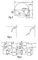
- FIG. 3 is an s-plane diagram in which a pole is denoted by a cross and a zero by a small circle.
- the diagram also shows that a pair of similar right-angled triangles can be constructed around the transfer function zero using the above results. As the triangles are similar the internal angle at the zero must be 90°, and therefore the zero must lie on the circle shown dashed.
- the parameter k determines the location of the zero on the circle, represented by the angle 0.
- k 0
- ⁇ 0 and the pole and zero of the transfer function coincide and therefore cancel. This is as should be expected, for if the amplifier gain is zero then the filter (K) can play no part in the response. As the amplifier gain is increased, 0 increases and results in an increasingly asymmetric lattice network transfer function.
- Figure 4 illustrates the notation to be used and the polyphase filter section to be considered, that is the feed forward section.
- the filter section pole will lie on the real axis, internal feedback loops can be applied to produce an asymmetrically placed pole as shown.
- the vectors represent complex numbers, and therefore normal rules for complex algebra apply.
- Any loop response pole position can be obtained for any given feed-forward section through appropriate choice of the feedback network gains, and so any transfer function can be realised.
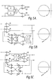
- the various classes of transfer function are obtained by taking the section output from different points around the loop as catalogued in Figures 5A to 5D which show the different transfer function options.
- V is to be large compared with U then the feedback parameters become very critical, so for practical circuits it is best to keep U and V comparable.
- Figure 5A illustrates the F networks only and the associated s-plane diagram illustrates that there is an asymmetric zero and a symmetric pole.
- the gain of the circuit is (1 +jk).
- Figure 5B illustrates a circuit which gives rise to the loop response only and the associated s-plane diagram shows that there is an asymmetric pole and a symmetric zero.
- the gain of the circuit is (Gk-1)- 1.
- Figure 5C illustrates the arrangement to give a complete closed loop response and the associated s-plane diagram shows both the pole and zero placed asymmetrically.
- the gain of the circuit is k(Gk-1)-'.
- FIG. 5D illustrates the intermediate response for a single pole K and the associated s-plane diagram shows that one has an asymmetric pole only, the gain being k(Gk-1 )-1.
- any complex transfer function comprising a pole and zero or single pole, can be implemented by applying polyphase feedback around polyphase filter.
- Higher order filters can easily be built up by cascading a number of these polyphase sections, for example to realise an elliptic SSB filter.
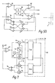
- Figure 6 illustrates in block schematic form a filter comprising at least two polyphase filter sections of the type illustrated in Figure 1 connected in cascade.
- the second filter section has been indicated with primed reference numerals. More than two filter sections can be connected in series if required.
- an important parameter which determines the sensitivity to component variations is the magnitude of the loop gain evaluated at the "image" frequency - the frequency which has the same value of ifrequencyl as the wanted signal but has the opposite sign - that is, the phase relationship between the polyphase paths is reversed.
- the loop gain at the image frequency is large, the circuit is insensitive to component mismatches between the I and Q channels in the feed forward part of the circuit, while if the loop gain is very much less than unity, then the circuit is insensitive to mismatch in the feedback portion of the circuit.
- FIG. 7 shows in greater detail the R.F. section of a radio receiver including a polyphase filter 60 made in accordance with the present invention.
- the circuit comprises a R.F. summing arrangement constituted by an amplifier 62 having one input connected to an antenna 63 and another input for a feedback signal from the polyphase filter 60.
- the output of the amplifier 62 is coupled to quadrature mixers 64, 66 which receive a reference signal from a local oscillator 68, that reference signal being supplied to the mixer 64 being phase shifted by ⁇ /2 in the phase shifter 70.
- a local oscillator frequency differ from the input carrier frequency by the desired output i.f., a low frequency signal is derived from each mixer 64, 66.
- the illustrated polyphase filter 60 comprises first and second signal paths I and Q which are connected to respective outputs of mixers 64 and 66.
- the filter 60 is constructed substantially as described previously with the revision that the feedback is implemented via an r.f. path. Accordingly the output from the I signal path is connected to another mixer 72 which receives the same reference signal as the mixer 64. Similarly the output from the Q signal path is connected to a further mixer 74 which receives the same reference frequency as the mixer 66.
- the outputs of the mixers 72, 74 are applied to a summing amplifier 76 whose output is fed back to the amplifier 62.
- An i.f. signal having an attenuated image is derived from a terminal 78 which is connected to a low frequency section of the filter 60.
- an input signal is applied to one input of the summing arrangement, that is, the amplifier 62, where it is summed with the feedback signal.
- the output of the amplifier 62 is applied to the quadrature pair of mixers 64, 66 which translate the signal down to i.f.
- the outputs of the quadrature pair of mixers 64, 66 then form the inputs to the polyphase filter F(w).
- the i.f. output is taken from the output of F(w).
- Figure 8 illustrates an embodiment of an SSB transmitter including a polyphase filter 80 made in accordance with the present invention.
- a source 82 of audio signals (a.f) is applied to a modulator 84 which is supplied with an i.f. signal ( ⁇ i.f. ) from a local oscillator 86. If the output of the modulator 84 is frequency up-converted to the final frequency by means of a single mixer, this operation would generate an image signal as well as a wanted signal. In the transmitter illustrated in Figure 8 this is avoided by the use of a quadrature pair of mixers 100, 102 in the feed forward path and another pair of mixers 96, 98 in the feedback path. An oscillator 106 provides the final frequency to the mixer 100, 102 to effect frequency up-conversion in the feed forward path and to the mixers 96, 98 to effect frequency down-conversion to the i.f. frequency in the feedback path.
- the input and feedback signals have been combined in the summing arrangement 12.
- a differencing arrangement can be used with the sign of the feedback circuit G(w) being reversed.
Landscapes
- Engineering & Computer Science (AREA)
- Power Engineering (AREA)
- Computer Networks & Wireless Communication (AREA)
- Signal Processing (AREA)
- Networks Using Active Elements (AREA)
- Superheterodyne Receivers (AREA)
- Noise Elimination (AREA)
- Transmitters (AREA)
Description
- The present invention relates to active polyphase filters and to a receiver and a transmitter including such filters.
- In many radio systems it is required to distinguish between a signal frequency that is above or below the frequency of a local oscillator and to attenuate one relative to the other. This filtering may either be implemented before the mixer, as in a superheterodyne receiver, or after it, as in some single sideband (SSB) receivers. In the latter approach at least two mixers must be employed, actuated by the modulating signals with distinct phases. This enables "positive" and "negative" frequency signals, produced by inputs above and below the local oscillator, to be distinguished. Polyphase filters can make use of multiple phase shifted inputs to produce asymmetric transfer functions. The use of polyphase networks in single sideband modulation is known from an article "Single Sideband Modulation using Sequence Asymmetric Polyphase Networks" by M. J. Gingell in Electrical Communication, Volume 48,
Number 1 and 2, 1973, pages 21 to 25. Normally the polyphase filters realise asymmetric zeros as opposed to asymmetric poles. Further unless polyphase filters are fabricated from close tolerance components then there is a risk of an unbalance between the channels. - Accordingly an object of the present invention is to provide a polyphase filter circuit which can easily realise asymmetric poles as well as asymmetric zeros and in which the effects of component tolerances is reduced.
- According to one aspect of the present invention there is provided a filter arrangement characterised by a polyphase filter having a set of paths therethrough for respective successively displaced phases of a signal, each said path being from a respective input to a respective output and being coupled to the next said path of the set so that said paths are coupled each to the next in sequence, a feedback path from each said output to the corresponding said input; means for injecting an input signal into a loop formed by a path through the filter and the corresponding said feedback path; and means for deriving an output signal from a loop formed by said path through the filter and said corresponding feedback path.
- The present invention also provides an active polyphase filter circuit characterised by a feed forward path filter having an input and an output for each phase, a feedback path polyphase filter having an input and an output for each said phase, the inputs of the feedback path filter being coupled to the respective corresponding outputs of the feed forward path filter, and the outputs of the feedback filter being coupled to the respective corresponding inputs of the feed forward path filter via respective combination means for combining the respective output signals of the feedback path filter with corresponding phases of an input signal, whereby a closed loop network is formed for each phase.
- In the present specification by an active polyphase filter is meant a filter which is implemented using amplifiers, for example operational amplifiers, to provide gain and to provide isolation between the impedances in different parts of the filter. The advantage of using active filter circuits is the ease of design of the filter and the circuit itself.
- By using a suitably chosen second polyphase filter to form the feedback path filter, the filter arrangement can be made generally insensitive to imbalance effects. Also the filter circuit can produce asymmetric poles as well as zeros. Further, in such arrangements, if the loop gain evaluated at the image frequency is larger then the circuit is insensitive to mismatch between the two I and Q paths in the feed forward section. However the circuit would still be sensitive to component mismatch in the feedback part of the filter. The problem of mismatch only arises when there are two I and Q paths so that by mixing to r.f. then the problem of mismatch is avoided.
- Lattice networks are known in the art and for example are discussed by C. Dillon in "Sensitivity considerations in cascaded lattice-type quadrature-modulation networks" IEE PROC. Vol. 128 Pt.G No. 4, August 1981, pages 154 to 157. In such circuits the number of paths is reduced to at least two by omitting two phases out of the four phases generally required and replacing them with an inverter. Thus the component count is reduced. In a practical application of such a simplified filter, a single sideband signal can be provided by feeding the filter arrangement in accordance with the present invention from a pair of quadrature mixers, the overall circuit behaviour being equivalent to a full four phase polyphase network. The network obtained will work, with a modified frequency response, for any phase angle between the channels.
- According to a second aspect of the present invention there is provided a circuit for providing rejection of the image signal produced at an intermediate frequency, characterised by first mixing means having a first input for an input signal, a second input coupled to local oscillator means and outputs for quadrature related signals (I and Q), at an intermediate frequency, a first two phase active filter for receiving said quadrature IF signals I and Q from said mixing means; and a second two phase active filter having first and second inputs connected to first and second outputs of said first active filter for producing first and second signals for remodulation by local oscillator means of a subsequent quadrature related mixing means for forming quadrature carrier signals having a frequency of the carrier of said input signal, and means for combining the quadrature carrier signals with said input signal to form the input signal to the first mixing means.
- According to a third aspect of the present invention there is provided a circuit for providing cancellation of an unwanted side band, characterised by means for providing an intermediate frequency signal by mixing an input signal with a local oscillator signal, a first polyphase active filter having a first input for receiving said intermediate frequency signal, and a second input; a feedback network comprising a polyphase active filter with first and second inputs, and first and second outputs, said second output connected with said first polyphase active filter second input; a summing means for combining a signal from said feedback network first output with said intermediate frequency signal; and means for supplying first and second signals from said first polyphase active filter to a frequency converter for generating a carrier signal, and for supplying first and second quadrature related signals derived from said carrier signal to said feedback network first and second inputs.
- The present invention will now be described, by way of example, with reference to the accompanying drawings, wherein:
- Figure 1 is a block schematic circuit diagram of an M-phase polyphase lattice filter arrangement made in accordance with the present invention,
- Figure 2 is an embodiment of Figure 1 for M = 2,
- Figure 3 is an s-plane diagram illustrating the lattice network transfer function,
- Figure 4 are s-plane diagrams illustrating the polyphase feedback vectors, the left hand diagram is of the feed forward section and the right hand diagram shows the loop response,
- Figures 5A to 5D illustrate the transfer function options with polyphase feedback,
- Figure 6 illustrates a filter comprising at least two polyphase filter sections connected in series,
- Figure 7 is a block schematic circuit diagram of a radio receiver including a polyphase filter in accordance with the present invention for use in image rejection, and
- Figure 8 is a block schematic circuit diagram of a single sideband (SSB) transmitter including a polyphase filter in accordance with the present invention for use in avoiding the generation of the unwanted sideband.
- In the drawings corresponding reference numerals have been used to indicate the same features.
- Referring to Figure 1 the polyphase filter arrangement comprises a first M-
phase polyphase filter 10 having aninput 12 and anoutput 14 for each of the M-phases. A twoinput summing amplifier 16 is connected to eachinput 12. One input of eachamplifier 16 is connected to receive a respective phase of an M-phase input A. The other input of each of theamplifiers 16 receives a feedback signal as will be described. - A second M-
phase polyphase filter 18 havingM inputs 20 andoutputs 22 provides a feedback loop with theinputs 20 connected to theoutputs 14 of corresponding phase of thefilter 10. Theoutputs 22 are connected torespective amplifiers 24 having a gain which amplifiers are connected to the respective other inputs of theamplifiers 16. - If the transfer functions of the
filters - then A' = A + β.G(ω).A"
- and A" = F(ω).A'
- [1 - β.F(ω). G(w)]A" = F(ω).A
- The overall transfer function is then:

- In general A"/A has zeros when F(ω) has zeros or G(ω) has poles.
- Also, in general A"/A has poles when [β.F(ω).G(ω)] = 1.
- Finally the transfer function A"/A has a regular value -[β.G(ω)]-1 when F(ω) has a pole.
- Since asymmetric zeros may easily be implemented in polyphase networks, asymmetric poles and zeros can be produced in the overall response. By suitably choosing F(ω), G(ω) and a a filter can be constructed in which the effects due to imbalance between paths are attenuated. These effects are an important consideration when rejection of an image signal by 60dB or so is required, as even 1% tolerance tends to limit the obtainable rejection to 40dB.
- Figure 2 is schematic circuit diagram of a filter arrangement which behaves as a four-phase arrangement but which has only two paths to which quadrature related signals are applied. This saving of paths is achieved by providing differencing or inverting
amplifiers 30 in thefilters amplifiers 32 as provided in the other paths. The construction of bothfilters filter 10 will be described in detail. - The
inputs filter 10 are connected bycircuits amplifiers circuits input 121 is cross connected by anothercircuit 38 to the inverting input of theamplifier 30 and theinput 122 is cross connected by anothercircuit 40 to a non-inverting input of theamplifier 32. The transfer function of thecircuits - The overall transfer function F(ω) of the
filter 10 is
- The
circuits - In the case of

filter 10 can be written as


- and radius =

- The parameter k determines the location of the zero on the circle, represented by the angle 0. The relationship between them can be found directly from the triangles, tan 0 =

this relationship also holds for d Δω if 0 is defined as the angle clockwise to the zero from the pole, as in Figure 3. There are several points which should be noted from Figure 3. Firstly if k = 0 then θ = 0 and the pole and zero of the transfer function coincide and therefore cancel. This is as should be expected, for if the amplifier gain is zero then the filter (K) can play no part in the response. As the amplifier gain is increased, 0 increases and results in an increasingly asymmetric lattice network transfer function. For small values of Θ the damping of the zero is insensitive to variations in amplifier gain. The most asymmetry occurs at Θ = 90°, corresponding to unity gain amplifiers (k = 1) which may of course be omitted. At this point the zero's frequency is equal to the radius of the circle, so we have
- As the amplifier gain increases further the K filter network increasingly dominates the lattice transfer function, and so the zero tends towards the original K filter network zero. It can also be seen that if the sign of the amplifier gain is reversed, this is topologically equivalent to interchanging the two polyphase signal paths. This has the effect of producing the transpose of the frequency response. In terms of the foregoing analysis the change of sign of k results in the change of sign of Θ, and so the positive and negative frequency responses are interchanged as required.
- For large K network zero damping, i.e. large d, these results tend towards the conclusion for the simple, pole only lattice network. As d increases the circle diameter increases, tending towards the vertical broken straight line through the pole, as in Figure 3. Then we have tan( Θ /2) ≃ tan 0, as Θ is small, and so with the identity

- Turning now to the effect of applying polyphase feedback, Figure 4 illustrates the notation to be used and the polyphase filter section to be considered, that is the feed forward section. Although in most cases the filter section pole will lie on the real axis, internal feedback loops can be applied to produce an asymmetrically placed pole as shown. The vectors represent complex numbers, and therefore normal rules for complex algebra apply. As an example the transfer function in Figure 3 would be represented in vector terminology as W= -Δω and U= -kγ-jγ.
- In the light of the results on the lattice network we will define

G(ω) = G = P + jQ the transfer function of the feedback network then if the loop response is L(ω), then L(ω)-1 = 1 - F(ω). G(ω),β = 1
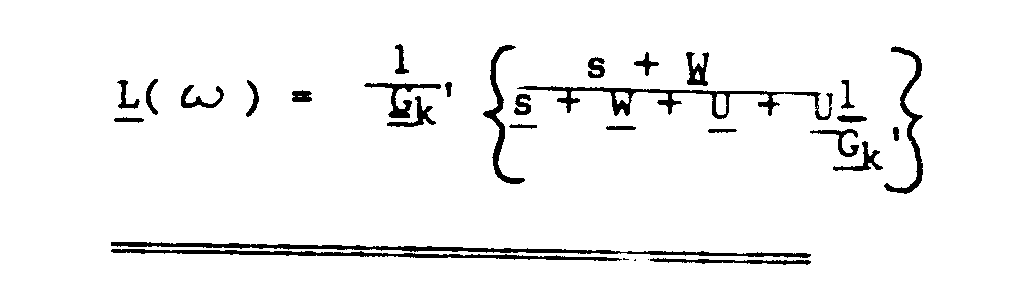

- Any loop response pole position can be obtained for any given feed-forward section through appropriate choice of the feedback network gains, and so any transfer function can be realised. The various classes of transfer function are obtained by taking the section output from different points around the loop as catalogued in Figures 5A to 5D which show the different transfer function options. However if V is to be large compared with U then the feedback parameters become very critical, so for practical circuits it is best to keep U and V comparable.
- Figure 5A illustrates the F networks only and the associated s-plane diagram illustrates that there is an asymmetric zero and a symmetric pole. The gain of the circuit is (1 +jk).
- Figure 5B illustrates a circuit which gives rise to the loop response only and the associated s-plane diagram shows that there is an asymmetric pole and a symmetric zero. The gain of the circuit is (Gk-1)-1.
- Figure 5C illustrates the arrangement to give a complete closed loop response and the associated s-plane diagram shows both the pole and zero placed asymmetrically. The gain of the circuit is k(Gk-1)-'.
- Finally Figure 5D illustrates the intermediate response for a single pole K and the associated s-plane diagram shows that one has an asymmetric pole only, the gain being k(Gk-1 )-1.
- The analyses have shown that any complex transfer function, comprising a pole and zero or single pole, can be implemented by applying polyphase feedback around polyphase filter. Higher order filters can easily be built up by cascading a number of these polyphase sections, for example to realise an elliptic SSB filter.
- Figure 6 illustrates in block schematic form a filter comprising at least two polyphase filter sections of the type illustrated in Figure 1 connected in cascade. For ease of reference the second filter section has been indicated with primed reference numerals. More than two filter sections can be connected in series if required.
- The parameters have been found not to be uniquely determined, so that they can be chosen either to simplify the circuit or to minimise the circuit's sensitivity to the component variations.
- Further it has been found that an important parameter which determines the sensitivity to component variations is the magnitude of the loop gain evaluated at the "image" frequency - the frequency which has the same value of ifrequencyl as the wanted signal but has the opposite sign - that is, the phase relationship between the polyphase paths is reversed. When the loop gain at the image frequency is large, the circuit is insensitive to component mismatches between the I and Q channels in the feed forward part of the circuit, while if the loop gain is very much less than unity, then the circuit is insensitive to mismatch in the feedback portion of the circuit.
- Figure 7 shows in greater detail the R.F. section of a radio receiver including a polyphase filter 60 made in accordance with the present invention. The circuit comprises a R.F. summing arrangement constituted by an
amplifier 62 having one input connected to anantenna 63 and another input for a feedback signal from the polyphase filter 60. The output of theamplifier 62 is coupled toquadrature mixers local oscillator 68, that reference signal being supplied to themixer 64 being phase shifted by π/2 in the phase shifter 70. By making the local oscillator frequency differ from the input carrier frequency by the desired output i.f., a low frequency signal is derived from eachmixer - The illustrated polyphase filter 60 comprises first and second signal paths I and Q which are connected to respective outputs of
mixers mixer 72 which receives the same reference signal as themixer 64. Similarly the output from the Q signal path is connected to afurther mixer 74 which receives the same reference frequency as themixer 66. The outputs of themixers amplifier 76 whose output is fed back to theamplifier 62. An i.f. signal having an attenuated image is derived from a terminal 78 which is connected to a low frequency section of the filter 60. - In operation, an input signal is applied to one input of the summing arrangement, that is, the
amplifier 62, where it is summed with the feedback signal. The output of theamplifier 62 is applied to the quadrature pair ofmixers mixers mixers amplifier 76. - Figure 8 illustrates an embodiment of an SSB transmitter including a
polyphase filter 80 made in accordance with the present invention. - A
source 82 of audio signals (a.f) is applied to amodulator 84 which is supplied with an i.f. signal (ωi.f.) from alocal oscillator 86. If the output of themodulator 84 is frequency up-converted to the final frequency by means of a single mixer, this operation would generate an image signal as well as a wanted signal. In the transmitter illustrated in Figure 8 this is avoided by the use of a quadrature pair ofmixers mixers oscillator 106 provides the final frequency to themixer mixers - In the illustrated embodiment of the present invention the input and feedback signals have been combined in the summing
arrangement 12. However if desired a differencing arrangement can be used with the sign of the feedback circuit G(w) being reversed.
On solution this gives:
which can be written A" [1 - β.F(ω).G(ω)]-1F(ω).A
Claims (7)
Applications Claiming Priority (2)
| Application Number | Priority Date | Filing Date | Title |
|---|---|---|---|
| GB08432011A GB2168868A (en) | 1984-12-19 | 1984-12-19 | Polyphase filters |
| GB8432011 | 1984-12-19 |
Publications (3)
| Publication Number | Publication Date |
|---|---|
| EP0185417A2 EP0185417A2 (en) | 1986-06-25 |
| EP0185417A3 EP0185417A3 (en) | 1988-02-10 |
| EP0185417B1 true EP0185417B1 (en) | 1992-02-05 |
Family
ID=10571406
Family Applications (1)
| Application Number | Title | Priority Date | Filing Date |
|---|---|---|---|
| EP19850201957 Expired - Lifetime EP0185417B1 (en) | 1984-12-19 | 1985-11-26 | Active polyphase filters |
Country Status (6)
| Country | Link |
|---|---|
| US (1) | US4723318A (en) |
| EP (1) | EP0185417B1 (en) |
| JP (1) | JPH0775329B2 (en) |
| KR (1) | KR920007090B1 (en) |
| DE (1) | DE3585366D1 (en) |
| GB (1) | GB2168868A (en) |
Families Citing this family (35)
| Publication number | Priority date | Publication date | Assignee | Title |
|---|---|---|---|---|
| FR2627336B1 (en) * | 1988-02-17 | 1990-06-08 | Thomson Csf | SWITCHABLE SELF-ADAPTIVE FILTER FOR RADIO TRANSMITTER AND / OR RECEIVER |
| NL8801412A (en) * | 1988-06-02 | 1990-01-02 | Philips Nv | ASYMMETRICAL POLYPHASE FILTER. |
| US5995818A (en) * | 1996-07-30 | 1999-11-30 | Trw Inc. | Low noise block downconverter |
| CN1126250C (en) | 1997-04-07 | 2003-10-29 | 皇家菲利浦电子有限公司 | Receiver and filter arrangement comprising polyphase filters |
| DE19727869C1 (en) * | 1997-06-30 | 1998-12-10 | Siemens Ag | Polyphase filter with adjustable transfer function |
| CN1160869C (en) * | 1997-09-25 | 2004-08-04 | 皇家菲利浦电子有限公司 | Improved phase receiver |
| US5973740A (en) * | 1997-10-27 | 1999-10-26 | International Business Machines Corporation | Multi-format reduced memory video decoder with adjustable polyphase expansion filter |
| US7555263B1 (en) | 1999-10-21 | 2009-06-30 | Broadcom Corporation | Adaptive radio transceiver |
| US8014724B2 (en) | 1999-10-21 | 2011-09-06 | Broadcom Corporation | System and method for signal limiting |
| US7082293B1 (en) * | 1999-10-21 | 2006-07-25 | Broadcom Corporation | Adaptive radio transceiver with CMOS offset PLL |
| US7299006B1 (en) * | 1999-10-21 | 2007-11-20 | Broadcom Corporation | Adaptive radio transceiver |
| US7558556B1 (en) | 1999-10-21 | 2009-07-07 | Broadcom Corporation | Adaptive radio transceiver with subsampling mixers |
| US6961546B1 (en) * | 1999-10-21 | 2005-11-01 | Broadcom Corporation | Adaptive radio transceiver with offset PLL with subsampling mixers |
| US7113744B1 (en) | 1999-10-21 | 2006-09-26 | Broadcom Corporation | Adaptive radio transceiver with a power amplifier |
| US6987966B1 (en) * | 1999-10-21 | 2006-01-17 | Broadcom Corporation | Adaptive radio transceiver with polyphase calibration |
| US7027792B1 (en) | 1999-11-23 | 2006-04-11 | Micro Linear Corporation | Topology for a single ended input dual balanced mixer |
| US7076217B1 (en) | 1999-11-23 | 2006-07-11 | Micro Linear Corporation | Integrated radio transceiver |
| US6987816B1 (en) | 1999-11-23 | 2006-01-17 | Micro Linear Corporation | Iris data recovery algorithms |
| US6441682B1 (en) * | 1999-11-23 | 2002-08-27 | Micro Linear Corporation | Active polyphase filter with transconductor cross-coupling of filter sections |
| US6445257B1 (en) | 1999-11-23 | 2002-09-03 | Micro Linear Corporation | Fuse-trimmed tank circuit for an integrated voltage-controlled oscillator |
| US6985541B1 (en) | 1999-11-23 | 2006-01-10 | Micor Linear Corporation | FM demodulator for a low IF receiver |
| US6198345B1 (en) * | 1999-12-21 | 2001-03-06 | Agilent Technologies, Inc. | Error reduction in quadrature polyphase filters with low open loop gain operational amplifiers |
| US6560449B1 (en) * | 2000-06-12 | 2003-05-06 | Broadcom Corporation | Image-rejection I/Q demodulators |
| US6778594B1 (en) | 2000-06-12 | 2004-08-17 | Broadcom Corporation | Receiver architecture employing low intermediate frequency and complex filtering |
| DE60130836T2 (en) * | 2000-06-12 | 2008-07-17 | Broadcom Corp., Irvine | Architecture and method for context switching |
| EP1348253B1 (en) * | 2000-12-18 | 2005-03-23 | Koninklijke Philips Electronics N.V. | GENERATING TWO SIGNALS HAVING A MUTUAL PHASE DIFFERENCE OF 90o |
| CN100426670C (en) * | 2002-08-15 | 2008-10-15 | 联发科技股份有限公司 | polyphase filter circuit |
| US7424281B1 (en) * | 2002-10-11 | 2008-09-09 | Maxim Integrated Products, Inc. | Image-rejection mixers having high linearity and high gain and RF circuits using the same |
| US7098731B1 (en) | 2004-01-13 | 2006-08-29 | Wyszynski Adam S | Synthesis method for an active polyphase filter |
| US7613249B1 (en) | 2004-04-21 | 2009-11-03 | Marvell International Ltd. | Spurious component reduction |
| US7196574B1 (en) | 2005-06-22 | 2007-03-27 | Vishinsky Adam S | Active polyphase ladder filters with transmission zeros and their synthesis method |
| US7733984B2 (en) * | 2006-11-08 | 2010-06-08 | International Business Machines Corporation | Implementing phase rotator circuits with embedded polyphase filter network stage |
| KR100954339B1 (en) * | 2008-09-10 | 2010-04-21 | 한국과학기술원 | Active-RCC Multiphase Band Filter Using Complex Zero Point |
| TWI422148B (en) * | 2009-12-10 | 2014-01-01 | Ralink Technology Corp | Complex filter and calibration method |
| US20260121592A1 (en) | 2024-10-28 | 2026-04-30 | Prodrive Technologies Innovation Services B.V. | Amplifier device with feedback and feed-forward control |
Family Cites Families (6)
| Publication number | Priority date | Publication date | Assignee | Title |
|---|---|---|---|---|
| GB1174709A (en) * | 1968-06-07 | 1969-12-17 | Standard Telephones Cables Ltd | A Symmetrical Polyphase Network |
| US3611165A (en) * | 1970-06-30 | 1971-10-05 | Nat Res Dev | Parallel pass and filters having multiple negative feedback paths |
| US3633117A (en) * | 1970-07-29 | 1972-01-04 | Itt | Suppression of a phase-sensitive spectral component from a signal |
| US3932818A (en) * | 1974-07-18 | 1976-01-13 | Hazeltine Corporation | Spectrum notcher |
| US4339727A (en) * | 1978-03-07 | 1982-07-13 | Nippon Electric Co., Ltd. | Waveform converting circuit |
| US4446438A (en) * | 1981-10-26 | 1984-05-01 | Gte Automatic Electric Incorporated | Switched capacitor n-path filter |
-
1984
- 1984-12-19 GB GB08432011A patent/GB2168868A/en not_active Withdrawn
-
1985
- 1985-11-26 EP EP19850201957 patent/EP0185417B1/en not_active Expired - Lifetime
- 1985-11-26 DE DE8585201957T patent/DE3585366D1/en not_active Expired - Lifetime
- 1985-12-16 KR KR1019850009432A patent/KR920007090B1/en not_active Expired
- 1985-12-16 US US06/809,538 patent/US4723318A/en not_active Expired - Fee Related
- 1985-12-16 JP JP60281231A patent/JPH0775329B2/en not_active Expired - Lifetime
Non-Patent Citations (1)
| Title |
|---|
| E. Philippow, TASCHENBUCH ELEKTROTECHNIK, Bd 3, 1978, VEB VERLAG, BERLIN, Seiten 823-825,847-849 * |
Also Published As
| Publication number | Publication date |
|---|---|
| EP0185417A2 (en) | 1986-06-25 |
| GB8432011D0 (en) | 1985-01-30 |
| KR920007090B1 (en) | 1992-08-24 |
| US4723318A (en) | 1988-02-02 |
| GB2168868A (en) | 1986-06-25 |
| KR860005504A (en) | 1986-07-23 |
| EP0185417A3 (en) | 1988-02-10 |
| JPH0775329B2 (en) | 1995-08-09 |
| JPS61148923A (en) | 1986-07-07 |
| DE3585366D1 (en) | 1992-03-19 |
Similar Documents
| Publication | Publication Date | Title |
|---|---|---|
| US4723318A (en) | Active polyphase filters | |
| EP0185416A2 (en) | Radio receiver/transmitter filters | |
| US6020783A (en) | RF notch filter having multiple notch and variable notch frequency characteristics | |
| EP0877476B1 (en) | Down conversion mixer | |
| KR100341231B1 (en) | Phase shifter | |
| US3423688A (en) | Hybrid-coupled amplifier | |
| US5051704A (en) | Feedforward distortion cancellation circuit | |
| US4806888A (en) | Monolithic vector modulator/complex weight using all-pass network | |
| JPH05243985A (en) | Vector lock loop | |
| EP0091378B1 (en) | Frequency conversion unit | |
| JPS59181864A (en) | Microwave receiving chain including direct microwave demodulator | |
| US3559042A (en) | Polyphase symmetrical network | |
| US3418595A (en) | Automatic frequency control system | |
| US3575660A (en) | Electronic image rejection apparatus | |
| US4673898A (en) | Wide band quadrature hybrid | |
| US6404255B1 (en) | Phase shift apparatus | |
| EP0973255B1 (en) | 90 degree phase shifter and image rejection mixer | |
| US7302011B1 (en) | Quadrature frequency doubling system | |
| US20070111679A1 (en) | Method and apparatus for vector signal processing | |
| US4075427A (en) | System for phase division multiplex duplex communication over a two-wire circuit between a master terminal and a slave terminal | |
| US20060073793A1 (en) | Local oscillator (LO) port linearization for communication system with ratiometric transmit path architecture | |
| US3737686A (en) | Shielded balanced microwave analog multiplier | |
| US2968716A (en) | Reduction of cross-modulation between the output stages of adjacent transmitters | |
| GB2210224A (en) | Mixer | |
| US4139823A (en) | Electrical energy transmission network |
Legal Events
| Date | Code | Title | Description |
|---|---|---|---|
| PUAI | Public reference made under article 153(3) epc to a published international application that has entered the european phase |
Free format text: ORIGINAL CODE: 0009012 |
|
| AK | Designated contracting states |
Kind code of ref document: A2 Designated state(s): DE FR GB SE |
|
| PUAL | Search report despatched |
Free format text: ORIGINAL CODE: 0009013 |
|
| AK | Designated contracting states |
Kind code of ref document: A3 Designated state(s): DE FR GB SE |
|
| RAP3 | Party data changed (applicant data changed or rights of an application transferred) |
Owner name: N.V. PHILIPS' GLOEILAMPENFABRIEKEN Owner name: PHILIPS ELECTRONIC AND ASSOCIATED INDUSTRIES LIMIT |
|
| 17P | Request for examination filed |
Effective date: 19880708 |
|
| 17Q | First examination report despatched |
Effective date: 19900727 |
|
| GRAA | (expected) grant |
Free format text: ORIGINAL CODE: 0009210 |
|
| AK | Designated contracting states |
Kind code of ref document: B1 Designated state(s): DE FR GB SE |
|
| REF | Corresponds to: |
Ref document number: 3585366 Country of ref document: DE Date of ref document: 19920319 |
|
| RAP4 | Party data changed (patent owner data changed or rights of a patent transferred) |
Owner name: N.V. PHILIPS' GLOEILAMPENFABRIEKEN Owner name: PHILIPS ELECTRONICS UK LIMITED |
|
| ET | Fr: translation filed | ||
| PLBE | No opposition filed within time limit |
Free format text: ORIGINAL CODE: 0009261 |
|
| STAA | Information on the status of an ep patent application or granted ep patent |
Free format text: STATUS: NO OPPOSITION FILED WITHIN TIME LIMIT |
|
| 26N | No opposition filed | ||
| PGFP | Annual fee paid to national office [announced via postgrant information from national office to epo] |
Ref country code: GB Payment date: 19941031 Year of fee payment: 10 |
|
| PGFP | Annual fee paid to national office [announced via postgrant information from national office to epo] |
Ref country code: SE Payment date: 19941124 Year of fee payment: 10 |
|
| PGFP | Annual fee paid to national office [announced via postgrant information from national office to epo] |
Ref country code: FR Payment date: 19941125 Year of fee payment: 10 |
|
| PGFP | Annual fee paid to national office [announced via postgrant information from national office to epo] |
Ref country code: DE Payment date: 19950124 Year of fee payment: 10 |
|
| EAL | Se: european patent in force in sweden |
Ref document number: 85201957.9 |
|
| REG | Reference to a national code |
Ref country code: FR Ref legal event code: CD |
|
| PG25 | Lapsed in a contracting state [announced via postgrant information from national office to epo] |
Ref country code: GB Effective date: 19951126 |
|
| PG25 | Lapsed in a contracting state [announced via postgrant information from national office to epo] |
Ref country code: SE Effective date: 19951127 |
|
| GBPC | Gb: european patent ceased through non-payment of renewal fee |
Effective date: 19951126 |
|
| PG25 | Lapsed in a contracting state [announced via postgrant information from national office to epo] |
Ref country code: FR Effective date: 19960731 |
|
| PG25 | Lapsed in a contracting state [announced via postgrant information from national office to epo] |
Ref country code: DE Effective date: 19960801 |
|
| EUG | Se: european patent has lapsed |
Ref document number: 85201957.9 |
|
| REG | Reference to a national code |
Ref country code: FR Ref legal event code: ST |