EP0184158A2 - Control unit for a microprogrammable processor - Google Patents
Control unit for a microprogrammable processor Download PDFInfo
- Publication number
- EP0184158A2 EP0184158A2 EP85115189A EP85115189A EP0184158A2 EP 0184158 A2 EP0184158 A2 EP 0184158A2 EP 85115189 A EP85115189 A EP 85115189A EP 85115189 A EP85115189 A EP 85115189A EP 0184158 A2 EP0184158 A2 EP 0184158A2
- Authority
- EP
- European Patent Office
- Prior art keywords
- microinstruction
- register
- instruction
- receive
- operatively connected
- Prior art date
- Legal status (The legal status is an assumption and is not a legal conclusion. Google has not performed a legal analysis and makes no representation as to the accuracy of the status listed.)
- Withdrawn
Links
Images


Classifications
-
- G—PHYSICS
- G06—COMPUTING; CALCULATING OR COUNTING
- G06F—ELECTRIC DIGITAL DATA PROCESSING
- G06F9/00—Arrangements for program control, e.g. control units
- G06F9/06—Arrangements for program control, e.g. control units using stored programs, i.e. using an internal store of processing equipment to receive or retain programs
- G06F9/22—Microcontrol or microprogram arrangements
- G06F9/223—Execution means for microinstructions irrespective of the microinstruction function, e.g. decoding of microinstructions and nanoinstructions; timing of microinstructions; programmable logic arrays; delays and fan-out problems
-
- G—PHYSICS
- G06—COMPUTING; CALCULATING OR COUNTING
- G06F—ELECTRIC DIGITAL DATA PROCESSING
- G06F9/00—Arrangements for program control, e.g. control units
- G06F9/06—Arrangements for program control, e.g. control units using stored programs, i.e. using an internal store of processing equipment to receive or retain programs
- G06F9/22—Microcontrol or microprogram arrangements
- G06F9/226—Microinstruction function, e.g. input/output microinstruction; diagnostic microinstruction; microinstruction format
-
- G—PHYSICS
- G06—COMPUTING; CALCULATING OR COUNTING
- G06F—ELECTRIC DIGITAL DATA PROCESSING
- G06F9/00—Arrangements for program control, e.g. control units
- G06F9/06—Arrangements for program control, e.g. control units using stored programs, i.e. using an internal store of processing equipment to receive or retain programs
- G06F9/30—Arrangements for executing machine instructions, e.g. instruction decode
- G06F9/30145—Instruction analysis, e.g. decoding, instruction word fields
-
- G—PHYSICS
- G06—COMPUTING; CALCULATING OR COUNTING
- G06F—ELECTRIC DIGITAL DATA PROCESSING
- G06F9/00—Arrangements for program control, e.g. control units
- G06F9/06—Arrangements for program control, e.g. control units using stored programs, i.e. using an internal store of processing equipment to receive or retain programs
- G06F9/30—Arrangements for executing machine instructions, e.g. instruction decode
- G06F9/30181—Instruction operation extension or modification
- G06F9/30185—Instruction operation extension or modification according to one or more bits in the instruction, e.g. prefix, sub-opcode
Definitions
- This invention relates to a processor, and more particularly, to a control unit which generates control signals for controlling the arithmetic and logic unit, in the execution of a microinstruction currently being held in a microinstruction register.
- Processors execute a variety of instructions, which can include arithmetic type instructions, shift type instructions, logical type instructions, data manipulative type instructions, .... These instructions can be categorized as memory-to-memory instructions, memory-to-register instructions, register-to-register instructions, ..., and as a result can be further classified as a type one instruction, type two instruction, ..., each type of instruction having a corresponding instruction format.
- a firmware program, or routine i.e., group of instructions
- a control store or control memory
- one of the firmware routines can be invoked and executed.
- the basic operation can be common to more than one macroinstruction, for example, "TEST BIT FOR A LOGIC VALUE OF 1', or "TEST BIT FOR A LOGIC VALUE OF 0'.
- a branch to the corresponding microprogram routine could be performed which would then execute the specific instruction and test the bit specified.
- This implementation requires several microinstructions to be executed and, requires these microinstructions to be stored in the control store.
- the present invention modifies the microinstruction as it is fetched from the control store and transferred to the microinstruction register. Predetermined fields of the microinstruction are modified with predetermined fields of the macro instruction which specifies the variation of the basic OP code, thereby modifying the basic operation, decreasing the execution time of the macro instruction, and resulting in speeding up the execution time of the macro instruction.
- the microprogrammable microprocessor includes a controller, an arithmetic and logig unit (ALU), and associated registers, for executing each instruction of a predefined instruction set, each instruction having an operand field and an operation code field.
- the controller of the present invention comprises a control store for storing a plurality of microinstructions.
- a translation element having input terminals adapted to receive the operand field of the instruction currently being executed, converts the information expressed by the format of the operand field of the instruction into information compatible with the format of the microinstruction word, thereby outputting converted operand data utilized to modify the microinstruction word as it is being fetched from the control store.
- a switching element having a first set of input terminals operatively connected to the control store to receive preselected portions of a fetched microinstruction, and further having a second set of input terminals operatively connected to the translation element to receive the converted operand data, selects between (i) the preselected portion of a fetched microinstruction word and (ii) the converted operand data, in response to a select signal, thereby outputting selected data.
- a register operatively connected to the switching element to receive the selected data, and further operatively connected to the control store to receive that portion of the fetched microinstruction word which is not subject to being selected by the switching element, holds the microinstruction for current execution.
- the present invention provides a control unit of a microprogrammable processor which modifies the microinstruction as it is fetched from control store with predetermihed fields from the macroinstruction.
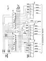
- FIG. 1 there is shown a block diagram of a microprogrammable microprocessor (or more simply microprocessor) 10 which can incorporate a control unit 20 of the present invention.
- the microprocessor 10 includes a memory data register (MD register) 101 and a memory address register (MA register) 102 which interfaces with a memory (not shown) via a memory bus 103.
- the microprocessor 10 of the preferred embodiment is an AQ type processor and includes an A register 104, a Q register (not shown), the Q register being a dedicated memory location, and a B register 105.
- a program counter 106 and a shift counter 107 are utilized in the overall control and execution of the instructions of the microprocessor 10.
- An ALU 110 executes the various arithmetic and logic operations under control of the control-unit 20.
- the ALU 110 is an 74F181 TTL integrated circuit chip.
- the A input and the B input of the ALU 110 are operatively coupled to receive the operand data from A register 104, B register 105, MD register 101, MA register 102, and data from a K-register 115 via a K bus through an A-MUX 111, and a B-MUX 112, respectively.
- the numbers 24 through the lines of the A input and the B input of ALU 110 indicate the number of bits of the line utilized in the preferred embodiment of the present invention, in this case the lines being a 24 bit line.
- Any bit in the A register 104 may be tested/manipulated through the use of a 24-to-1 A-register multiplexer (24-to-1 A-REG MUX) 113 and a 1 of 24 bit mask 114.
- the control unit 20 of the preferred embodiment of the present invention includes a 48 bit wide control ROM 201 which stores the microinstructions utilized to implement the macro instruction set of the microprocessor 10.
- the control ROM 201 also includes as part of the microinstruction a constant which is obtained from a constant PROM 203 in the execution of some of the microinstructions. Twelve bits from the control ROM 201 are coupled to a first input of a MUX 202. A second group of 12 bits is coupled from a field programmable logic array (FPLA) 204 to a second input of the MUX 202.
- the 12 bit output of the MUX 202 is coupled to a microinstruction register 205, along with 36 bits from the control ROM 201.
- FPLA field programmable logic array
- the outputs of the microinstruction register 205 in conjunction with a decoder 206 comprise the control signals which are in turn coupled to the various units, such as the ALU 110, for controlling the operation of these units.
- SELECT(206) By selecting the second inputs of MUX 202 via a select signal, SELECT(206), predetermined bits of the microinstruction read from control ROM 201 can be modified thereby giving the microinstruction transmitted to the microinsruction register 205 a different (or modified) set of control indicators, yielding a modified set of control signals for a modified operation.
- the 12 bits of the microinstruction which are modified are in part determined from the operand field of the macroinstruction.
- the operand field temporarily stored in the MA register 102 is coupled to the FPLA 204 which decodes the operand data into control bits of the microinstruction.
- the control ROM 201 is addressed by bits 1-12 of the MA register 101, a "next instruction address" field of the microinstruction, or from an address supplied by a macro OP code register (OP-CODE register) 120.
- test flip-flop control logic 207 and test flip-flop 208 are included.
- Four bits from the FPLA 204 are coupled to the test flip-flop control logic 207 along with an ALU TEST OUTPUT signal from ALU 110 and the output signal of the 24-to-l A-REG MUX 113.
- the microprocessor 10 of the preferred embodiment of the present invention has defined five instruction types as shown in Table 1. Of particular interest here in the Type 1 instruction which utilizes the modification feature of the control unit of the present invention. Before discussing the operations required by the microprocessor 10 in the execution of the Type 1 instruction, some general discussion of the microprocessor 10 will be given.
- FIG. 2 there is shown an instruction format of a Type 1 instruction word.
- the microprocessor 10 of the preferred embodiment of the present invention utilizes a 24 bit instruction word.
- the upper six bits (bits 18-23) are utilized for the macro OP code.
- bits 15-17 are utilized for specifying an index register.
- Bits 0-14 define an operand field.
- the operand defines the memory address of the operand data.
- the R field defines a variation of the basic operation of the OP code.
- the test field (bit 5) defines whether a test operation is involved, and the K field (bits 0-4) specify the bit to be tested.
- the effective bit to be tested is a function of the K field and the index field since the K field is subject to an indexing operation.
- Figure 3 shows a format of the microinstruction word of the microprocessor 10 of the preferred embodiment of the present invention.
- the modification bits are supplied by the FPLA 204.
- Bits 35-40 and bits 8-13 of the microinstruction word are modified by the FPLA 204.
- Bits 35 - 39 of the microinstruction word are utilized for the control of the ALU 10, and bit 40 of the microinstruction word is utilized for the destination of the A LU , bit 40 specifying the A register 104.
- the next microinstruction address is provided by bits 6-17 of the microinstruction word.
- the lower 18 bits of the instruction are now contained in the MA register 102.
- the memory address is now stored in the memory address register.
- the lower 15 bits of the MA register 102 are transmitted to the FPLA 204.
- the lower 5 bits of the MA register 102 are also used to select the input to the 24-to-1 A register multiplexer 103 and the mask to be outputted by the 1 of 24 bit mask 114.
- the first microinstruction specifies SELECT(206). This allows the next microinstruction that is currently being fetched to be modified by the output of the FPLA 204.
- the microinstruction that is being fetched and modified always specifies the A register and the K bus as sources and the B register as one of the destinations.
- the FPLA 204 outputs 12 bits which are substituted or used to set 13 of the bits in the microinstruction. Five of the FPLA outputs are substituted for bits 35-39 of the microinstruction. These bits, define the ALU operation to be performed. One FPLA output is substituted for bit 40 in the microinstruction and this bit determines if the A register will be a destination for the ALU 110 output. The five remaining output bits of the FPLA 204 are substituted for bits 8-12 of the microinstruction. These bits form part of the next microinstruction and are used to vector firmware to various routines required to complete the execution of various Type 1 instructions.
- the ALU 10 operation will be changed to the appropriate operation.
- the majority of the Type 1 instructions will be completed when the modified microinstruction has completed its execution.
- the Type 1 instructions that have not been completed will be vectored by the modified microinstruction to an appropriate routine that will complete that specific Type 1 instruction.
- FIG. 4 there is shown a logic diagram of the FPLA 204, and the MUX 202.
- the FPLA 204 is divided into two individual FPLAs, FPLA-1 250 and FPLA-2 251.
- the inputs of each FPLA 250, 251 are numbered from I 00 through I 15 , each input coupled to a corresponding input bit MA 00 - MA 14 from the memory address register 102, the memory address register being used to temporarily store the operand field of the Type 1 macroinstruction.
- I 15 of each FPLA 250, 251 is a combined input of MA03 and MA 0 4.
- the input I 15 is utilized as a check on the K field in which a value of logic 0 indicates the value of K must be less than or equal to 23, a logic 1 indicates the K field must have a value of greater than or equal to 24, or if no value is specified K is a don't care term.
- the FPLAs 250, 251 can be of the type 82S100 integrated circuit chip.
- the MUX 202 of the preferred embodiment of the present invention comprises three integrated circuit chips of the type F157, denoted 222, 223, 224. Each zero input of the MUX 202 is coupled to a corresponding output Foo through F 05 of the FPLAs 250, 251 as shown.
- Each one input of the MUX 202 is coupled to a corresponding bit CR 08 through CR 13 , and CR 35 through CR 40 of the control ROM 201 (CR 08 denoting bit 8 of the control ROM, CR 09 denoting bit 9 of the control ROM).
- the output of the MUX 202 is then coupled to a corresponding bit of the microinstruction register, MIR40 denoting bit 40 of the microinstruction register 205, MIR39 denoting bit 39 of the microinstruction register 205, ....
- Output F 05 of PLA 251 is combined with bit 32 of the next microinstruction if SELECT(206) is enabled in the current microinstruction.
- This operation is used to change a function of the microinstruction word to a Type 1 shift operation.
- Bits 0 - 14 of the Type 1 instruction are utilized to generate the modification bits of the microinstruction word in accordance with Tables 2 and 3.
- the letter L indicates low (or a logic zero) and the letter B indicates high (or a logic one).
- the letter A indicates active, the preferred embodiment of the present invention utilizes active high.
- the dot and the dash indicate not present and don't care, respectively.
- the decoder 206 comprises a plurality of decoder integrated circuit chips.
- a first 3-t0-8 decoder 306 has coupled to the inputs the outputs of the microinstruction register 205, the output of the microinstruction register 205 being denoted OMIRXX where XX denotes the bit of the microinstruction register.
- a second 3-to-8 decoder 307 is utilized to generate the ENABLE(230) signal, the second decoder decoding the output bits from the microinstruction register 205 as shown.
- the first and second decoders 306, 307 are of the type F138 integrated circuit chip.
- the control ROM 201 is of the type AMD AM 275191, and the microinstruction register 205 is of the type 74F175 integrated circuit chip.
- the test flip flop control logic 207 is implemented in accordance with the truth table of Figure 6, from the output signals F 6 and F 7 from the FPLAs 250, 251.
- the data manipulation and bit testing instructions implemented in the microprocessor 10 of the preferred embodiment of the present invention are listed in the Appendix along with a brief description of the function performed by the instruction.
Abstract
Description
- This invention relates to a processor, and more particularly, to a control unit which generates control signals for controlling the arithmetic and logic unit, in the execution of a microinstruction currently being held in a microinstruction register.
- Processors execute a variety of instructions, which can include arithmetic type instructions, shift type instructions, logical type instructions, data manipulative type instructions, .... These instructions can be categorized as memory-to-memory instructions, memory-to-register instructions, register-to-register instructions, ..., and as a result can be further classified as a type one instruction, type two instruction, ..., each type of instruction having a corresponding instruction format. Various approaches currently exist for executing a macro instruction in a microprogrammable microprocessor. In one such implementation, a firmware program, or routine (i.e., group of instructions) can reside in a control store (or control memory) which stores the group of microinstructions. When the operation code (OP code) of a macro instruction is initially decoded, one of the firmware routines can be invoked and executed. For a predetermined type of macro instruction, such as the data manipulative type macro instruction, the basic operation can be common to more than one macroinstruction, for example, "TEST BIT FOR A LOGIC VALUE OF 1', or "TEST BIT FOR A LOGIC VALUE OF 0'. Based on the specific instruction, a branch to the corresponding microprogram routine could be performed which would then execute the specific instruction and test the bit specified. This implementation requires several microinstructions to be executed and, requires these microinstructions to be stored in the control store.
- In an effort to reduce the size of the control store and to reduce the number of instructions required to be executed in the execution of the macro instruction resulting in a faster execution time, the present invention modifies the microinstruction as it is fetched from the control store and transferred to the microinstruction register. Predetermined fields of the microinstruction are modified with predetermined fields of the macro instruction which specifies the variation of the basic OP code, thereby modifying the basic operation, decreasing the execution time of the macro instruction, and resulting in speeding up the execution time of the macro instruction.
- According.to the present invention the microprogrammable microprocessor includes a controller, an arithmetic and logig unit (ALU), and associated registers, for executing each instruction of a predefined instruction set, each instruction having an operand field and an operation code field. The controller of the present invention comprises a control store for storing a plurality of microinstructions. A translation element, having input terminals adapted to receive the operand field of the instruction currently being executed, converts the information expressed by the format of the operand field of the instruction into information compatible with the format of the microinstruction word, thereby outputting converted operand data utilized to modify the microinstruction word as it is being fetched from the control store. A switching element, having a first set of input terminals operatively connected to the control store to receive preselected portions of a fetched microinstruction, and further having a second set of input terminals operatively connected to the translation element to receive the converted operand data, selects between (i) the preselected portion of a fetched microinstruction word and (ii) the converted operand data, in response to a select signal, thereby outputting selected data. A register, operatively connected to the switching element to receive the selected data, and further operatively connected to the control store to receive that portion of the fetched microinstruction word which is not subject to being selected by the switching element, holds the microinstruction for current execution.
- The present invention provides a control unit of a microprogrammable processor which modifies the microinstruction as it is fetched from control store with predetermihed fields from the macroinstruction.
- These and other details of the present invention will become more apparent when taken in conjunction with the following description and attached drawings, wherein like characters indicate like parts, and which drawings form a part of the present application.
-
- Fig. 1 shows a block diagram of a microprogrammable microprocessor which incorporates a control unit of the present invention;
- Figure 2 shows an instruction format of a data manipulative/test bit instruction of the processor of Figure 1;
- Figure 3 shows a format of a microinstructions word of the processor of Figure 1;
- Figure 4 shows a logic diagram of a programmable logic array of the controller of the preferred embodiment of the present invention;
- Figure 5 shows a partial logic diagram of,a decoder of the controller of the preferred embodiment of the present invention; and
- Figure 6 shows the truth table utilized for the implementation of control logic for a test flip/flop of the controller of the preferred embodiment of the present invention.
- Referring to Figure 1, there is shown a block diagram of a microprogrammable microprocessor (or more simply microprocessor) 10 which can incorporate a
control unit 20 of the present invention. Themicroprocessor 10 includes a memory data register (MD register) 101 and a memory address register (MA register) 102 which interfaces with a memory (not shown) via a memory bus 103. Themicroprocessor 10 of the preferred embodiment is an AQ type processor and includes anA register 104, a Q register (not shown), the Q register being a dedicated memory location, and aB register 105. Aprogram counter 106 and ashift counter 107 are utilized in the overall control and execution of the instructions of themicroprocessor 10. An ALU 110 executes the various arithmetic and logic operations under control of the control-unit 20. In the preferred embodiment of the present invention, the ALU 110 is an 74F181 TTL integrated circuit chip. The A input and the B input of theALU 110 are operatively coupled to receive the operand data fromA register 104,B register 105, MD register 101,MA register 102, and data from a K-register 115 via a K bus through an A-MUX 111, and a B-MUX 112, respectively. (Thenumbers 24 through the lines of the A input and the B input ofALU 110 indicate the number of bits of the line utilized in the preferred embodiment of the present invention, in this case the lines being a 24 bit line. This nomenclature is included in the drawings of the present application.) Any bit in theA register 104 may be tested/manipulated through the use of a 24-to-1 A-register multiplexer (24-to-1 A-REG MUX) 113 and a 1 of 24bit mask 114. - The
control unit 20 of the preferred embodiment of the present invention includes a 48 bitwide control ROM 201 which stores the microinstructions utilized to implement the macro instruction set of themicroprocessor 10. Thecontrol ROM 201 also includes as part of the microinstruction a constant which is obtained from aconstant PROM 203 in the execution of some of the microinstructions. Twelve bits from thecontrol ROM 201 are coupled to a first input of aMUX 202. A second group of 12 bits is coupled from a field programmable logic array (FPLA) 204 to a second input of theMUX 202. The 12 bit output of theMUX 202 is coupled to amicroinstruction register 205, along with 36 bits from thecontrol ROM 201. The outputs of themicroinstruction register 205 in conjunction with adecoder 206 comprise the control signals which are in turn coupled to the various units, such as theALU 110, for controlling the operation of these units. By selecting the second inputs ofMUX 202 via a select signal, SELECT(206), predetermined bits of the microinstruction read fromcontrol ROM 201 can be modified thereby giving the microinstruction transmitted to the microinsruction register 205 a different (or modified) set of control indicators, yielding a modified set of control signals for a modified operation. The 12 bits of the microinstruction which are modified are in part determined from the operand field of the macroinstruction. The operand field temporarily stored in theMA register 102 is coupled to the FPLA 204 which decodes the operand data into control bits of the microinstruction. Thecontrol ROM 201 is addressed by bits 1-12 of the MA register 101, a "next instruction address" field of the microinstruction, or from an address supplied by a macro OP code register (OP-CODE register) 120. - Since the preferred embodiment of the present invention is implemented for data manipulative/bit test type instructions, a test flip-flop control logic. 207 and test flip-
flop 208 are included. Four bits from theFPLA 204 are coupled to the test flip-flop control logic 207 along with an ALU TEST OUTPUT signal fromALU 110 and the output signal of the 24-to-l A-REG MUX 113. - The
microprocessor 10 of the preferred embodiment of the present invention has defined five instruction types as shown in Table 1.
Type 1 instruction which utilizes the modification feature of the control unit of the present invention. Before discussing the operations required by themicroprocessor 10 in the execution of theType 1 instruction, some general discussion of themicroprocessor 10 will be given. - Referring to Figure 2, there is shown an instruction format of a
Type 1 instruction word. Themicroprocessor 10 of the preferred embodiment of the present invention utilizes a 24 bit instruction word. The upper six bits (bits 18-23) are utilized for the macro OP code. For those instructions which can be indexed, bits 15-17 are utilized for specifying an index register. Bits 0-14 define an operand field. For aType 4 instruction, the operand defines the memory address of the operand data. For aType 1 instruction the R field defines a variation of the basic operation of the OP code. The test field (bit 5) defines whether a test operation is involved, and the K field (bits 0-4) specify the bit to be tested. The effective bit to be tested is a function of the K field and the index field since the K field is subject to an indexing operation. - Figure 3 shows a format of the microinstruction word of the
microprocessor 10 of the preferred embodiment of the present invention. The modification bits are supplied by the FPLA 204. Bits 35-40 and bits 8-13 of the microinstruction word are modified by the FPLA 204. Bits 35 - 39 of the microinstruction word are utilized for the control of theALU 10, andbit 40 of the microinstruction word is utilized for the destination of the ALU,bit 40 specifying theA register 104. The next microinstruction address is provided by bits 6-17 of the microinstruction word. - The basic operation of the
microprocessor 10 will now be discussed. During a first cycle of a microporcessor 10 an instruction is fetched from the memory (not shown) and is placed into the memory data register 101. The upper six bits (bits 18-23) are also placed in theOP code register 120. These six bits comprise the basic instruction (or MACRO) OP code. As part of this first cycle, the instruction undergoes any address or instruction modification that might result from relative addressing or indexing. The ,result of this operation is then stored in thememory address register 102. Based on the OP code supplied byOP code register 120, the firmware routines stored incontrol ROM 201 execute a 64 way branch based on the contents of theOP code register 120. This vectors the firmware to the routine required to execute any one of the 64 basic OP codes of themicroprocessor 10. The operations described thus far are common to the execution of all of the instructions of themicroprocessor 10. - The lower 18 bits of the instruction are now contained in the
MA register 102. For an instruction which requires an operand data fetch from memory, the memory address is now stored in the memory address register. For aType 1 instruction the lower 15 bits of theMA register 102 are transmitted to theFPLA 204. The lower 5 bits of theMA register 102 are also used to select the input to the 24-to-1 A register multiplexer 103 and the mask to be outputted by the 1 of 24bit mask 114. The first microinstruction specifies SELECT(206). This allows the next microinstruction that is currently being fetched to be modified by the output of theFPLA 204. The microinstruction that is being fetched and modified always specifies the A register and the K bus as sources and the B register as one of the destinations. TheFPLA 204outputs 12 bits which are substituted or used to set 13 of the bits in the microinstruction. Five of the FPLA outputs are substituted for bits 35-39 of the microinstruction. These bits, define the ALU operation to be performed. One FPLA output is substituted forbit 40 in the microinstruction and this bit determines if the A register will be a destination for theALU 110 output. The five remaining output bits of theFPLA 204 are substituted for bits 8-12 of the microinstruction. These bits form part of the next microinstruction and are used to vector firmware to various routines required to complete the execution ofvarious Type 1 instructions. As a result of modifying the microinstruction fetched and transmitted to themicroinstruction register 205, theALU 10 operation will be changed to the appropriate operation. The majority of theType 1 instructions will be completed when the modified microinstruction has completed its execution. TheType 1 instructions that have not been completed will be vectored by the modified microinstruction to an appropriate routine that will complete thatspecific Type 1 instruction. - Referring to Figure 4 there is shown a logic diagram of the
FPLA 204, and theMUX 202. TheFPLA 204 is divided into two individual FPLAs, FPLA-1 250 and FPLA-2 251. The inputs of eachFPLA memory address register 102, the memory address register being used to temporarily store the operand field of theType 1 macroinstruction. I15 of eachFPLA MA 04. The input I15 is utilized as a check on the K field in which a value oflogic 0 indicates the value of K must be less than or equal to 23, alogic 1 indicates the K field must have a value of greater than or equal to 24, or if no value is specified K is a don't care term. TheFPLAs MUX 202 of the preferred embodiment of the present invention comprises three integrated circuit chips of the type F157, denoted 222, 223, 224. Each zero input of theMUX 202 is coupled to a corresponding output Foo through F05 of theFPLAs MUX 202 is coupled to a corresponding bit CR08 through CR13, and CR35 through CR40 of the control ROM 201 (CR08 denoting bit 8 of the control ROM, CR09 denoting bit 9 of the control ROM...). The output of theMUX 202 is then coupled to a corresponding bit of the microinstruction register,MIR40 denoting bit 40 of themicroinstruction register 205,MIR39 denoting bit 39 of themicroinstruction register 205, .... Output F05 ofPLA 251 is combined withbit 32 of the next microinstruction if SELECT(206) is enabled in the current microinstruction. This operation is used to change a function of the microinstruction word to aType 1 shift operation. Bits 0 - 14 of theType 1 instruction are utilized to generate the modification bits of the microinstruction word in accordance with Tables 2 and 3. (The letter L indicates low (or a logic zero) and the letter B indicates high (or a logic one). The letter A indicates active, the preferred embodiment of the present invention utilizes active high. The dot and the dash indicate not present and don't care, respectively.)

- Referring to Figure 5 there is shown a partial logic diagram of the
decoder 206. Thedecoder 206 comprises a plurality of decoder integrated circuit chips. A first 3-t0-8decoder 306 has coupled to the inputs the outputs of themicroinstruction register 205, the output of themicroinstruction register 205 being denoted OMIRXX where XX denotes the bit of the microinstruction register. A second 3-to-8decoder 307 is utilized to generate the ENABLE(230) signal, the second decoder decoding the output bits from themicroinstruction register 205 as shown. The first andsecond decoders - The
control ROM 201 is of the type AMD AM 275191, and themicroinstruction register 205 is of the type 74F175 integrated circuit chip. The test flipflop control logic 207 is implemented in accordance with the truth table of Figure 6, from the output signals F6 and F7 from theFPLAs microprocessor 10 of the preferred embodiment of the present invention are listed in the Appendix along with a brief description of the function performed by the instruction. - While there has been shown what is considered to be the preferred embodiment of the present invention, it will be manifest that many changes and modifications can be made therein without departing from the essential spirit and scope of the invention.


Claims (7)
- A control unit (20) for a microprogrammable processor (10) which includes an arithmetic and logic unit (ALU110) and associated registers (101,102,104,105,...) for executing each instruction of a predefined instruction set, each instruction having an operand field and an operation code field, characterized in that said controller (20) comprises:a) control store means (201,203) for storing a plurality of microinstructions;b) translation means (204), having input terminals adapted to receive the operand field of the instruction currently being executed, for converting the information expressed by the format of the operand field of the instruction into information compatible with the format of the microinstruction word, thereby outputting converted operand data utilized to modify the microinstruction word as it is being fetched from the control store means (201,203);c) switching means (202), having a first set of input terminals operatively connected to said control store means (201,203) to receive preselected portions of a fetched microinstruction., and further having a second set of input terminals operatively connected to said translation means to receive said converted operand data, for selecting between (i) the preselected portion of a fetched microinstruction word and (ii) the converted operand data, in response to a select signal, thereby outputting selected data; andd) register means (205) operatively connected to said switching means (202) to receive the selected data, and further operatively connected to said control store means (201,203) to receive that portion of the fetched microinstruction word which is not subject to being selected by said switching means, for holding the microinstruction for current execution.
- 2. A uP-controller, according to Claim 1, further characterized by decoder means (206), operatively connected to said register means (205), for decoding preselected bits of said register means to generate a second set of control signals, including the select signal, thereby providing partial control of said ALU (110) and said associated registers (101,102,104,105).
- 3. A uP-controller, according to Claim 2, characterized by logic means (207,208) operatively connected to said translation means (204), and further having a first input terminal adapted to receive a first condition signal indicating a condition of a preselected bit and having a second input terminal adapted to receive a second condition signal indicating a condition of a test output of said ALU, for providing a test signal indicating the results of a tested condition resulting from the execution of said microinstruction.
- µP-controller, according to Claim 1, characterized in that said control store means (201,203) comprises:a) a first control store (201) for storing a plurality of microinstructions subject to decoding; andb) a second control store (203) operatively connected to said ALU (110), for storing constant digital values corrsponding to said microinstructions.
- 5. A µP-controller according to Claim 2 or one of the subsequent claims, whereat the register means (205) output a first set of control signals and the decoder means (206) generate the second set of control signals, including the select signal, characterized in that said first and second set of control signals provide control of said ALU (110) and said associated registers (101,102,104,105).
- 6. A µP-controller according to one of the preceding claims, characterized by holding means (205,206), operatively connected to said switching means (202) to receive the selected data, and further operatively connected to said control store means (201,203) to receive that portion of the fetched microinstruction word which is not subject to being selected by said switching means, for providing control signals to said ALU (110) and associated registers (101,102,104,105) for the microinstruction currently being executed.
- 7. A µP-controller according to one of the prededing claims, characterized in that the switching means (202) includes a multiplexer.
Applications Claiming Priority (2)
| Application Number | Priority Date | Filing Date | Title |
|---|---|---|---|
| US06/678,536 US4825363A (en) | 1984-12-05 | 1984-12-05 | Apparatus for modifying microinstructions of a microprogrammed processor |
| US678536 | 1984-12-05 |
Publications (2)
| Publication Number | Publication Date |
|---|---|
| EP0184158A2 true EP0184158A2 (en) | 1986-06-11 |
| EP0184158A3 EP0184158A3 (en) | 1987-05-27 |
Family
ID=24723212
Family Applications (1)
| Application Number | Title | Priority Date | Filing Date |
|---|---|---|---|
| EP85115189A Withdrawn EP0184158A3 (en) | 1984-12-05 | 1985-11-29 | Control unit for a microprogrammable processor |
Country Status (6)
| Country | Link |
|---|---|
| US (1) | US4825363A (en) |
| EP (1) | EP0184158A3 (en) |
| JP (1) | JPH0812598B2 (en) |
| AU (1) | AU584642B2 (en) |
| CA (1) | CA1242801A (en) |
| NO (1) | NO169924C (en) |
Cited By (5)
| Publication number | Priority date | Publication date | Assignee | Title |
|---|---|---|---|---|
| EP0333153A2 (en) * | 1988-03-15 | 1989-09-20 | Kabushiki Kaisha Toshiba | Self-test circuit of information processor |
| GB2215879A (en) * | 1988-03-23 | 1989-09-27 | Benchmark Technologies | Numerical processor using microcode |
| EP0356940A2 (en) * | 1988-08-29 | 1990-03-07 | Matsushita Electric Industrial Co., Ltd. | Finite state machine |
| EP0397414A2 (en) * | 1989-05-08 | 1990-11-14 | Matsushita Electric Industrial Co., Ltd. | Control device having a function of modifying a microinstruction |
| EP0498067A2 (en) * | 1991-02-08 | 1992-08-12 | International Business Machines Corporation | Microcode generation for a scalable compound instruction set machine |
Families Citing this family (22)
| Publication number | Priority date | Publication date | Assignee | Title |
|---|---|---|---|---|
| DE3650602T2 (en) * | 1985-04-08 | 1997-06-12 | Hitachi Ltd | Data processing system |
| US5155819A (en) * | 1987-11-03 | 1992-10-13 | Lsi Logic Corporation | Flexible ASIC microcomputer permitting the modular modification of dedicated functions and macroinstructions |
| DE68927783T2 (en) * | 1988-05-03 | 1997-09-25 | Wang Laboratories | MICROPROCESSOR WITH EXTERNAL CONTROL MEMORY |
| JP2901081B2 (en) * | 1989-12-19 | 1999-06-02 | 株式会社日立製作所 | How to rename non-leaf entries in OSI directory |
| US5241637A (en) * | 1990-01-05 | 1993-08-31 | Motorola, Inc. | Data processor microsequencer having multiple microaddress sources and next microaddress source selection |
| US5276824A (en) * | 1990-01-08 | 1994-01-04 | Motorola, Inc. | Data processor having a multi-stage instruction pipe and selection logic responsive to an instruction decoder for selecting one stage of the instruction pipe |
| US5412785A (en) * | 1990-04-09 | 1995-05-02 | Motorola, Inc. | Microprogrammed data processor which includes a microsequencer in which a next microaddress output of a microROM is connected to the or-plane of an entry PLA |
| US5280595A (en) * | 1990-10-05 | 1994-01-18 | Bull Hn Information Systems Inc. | State machine for executing commands within a minimum number of cycles by accomodating unforseen time dependency according to status signals received from different functional sections |
| US5452423A (en) * | 1991-06-13 | 1995-09-19 | Chips And Technologies, Inc. | Two-ROM multibyte microcode address selection method and apparatus |
| US5379392A (en) * | 1991-12-17 | 1995-01-03 | Unisys Corporation | Method of and apparatus for rapidly loading addressing registers |
| US5414821A (en) * | 1991-12-17 | 1995-05-09 | Unisys Corporation | Method of and apparatus for rapidly loading addressing environment by checking and loading multiple registers using a specialized instruction |
| US5559974A (en) * | 1994-03-01 | 1996-09-24 | Intel Corporation | Decoder having independently loaded micro-alias and macro-alias registers accessible simultaneously by one micro-operation |
| US5581720A (en) * | 1994-04-15 | 1996-12-03 | David Sarnoff Research Center, Inc. | Apparatus and method for updating information in a microcode instruction |
| US5734817A (en) * | 1995-03-01 | 1998-03-31 | Unisys Corporation | Method for making a data base available to a user program during data base recovery |
| US5761740A (en) * | 1995-11-30 | 1998-06-02 | Unisys Corporation | Method of and apparatus for rapidly loading addressing registers |
| US5884071A (en) * | 1997-03-31 | 1999-03-16 | Intel Corporation | Method and apparatus for decoding enhancement instructions using alias encodings |
| US6643800B1 (en) * | 2000-02-02 | 2003-11-04 | Hewlett-Packard Development Company, L.P. | Method and apparatus for testing microarchitectural features by using tests written in microcode |
| US7181484B2 (en) * | 2001-02-21 | 2007-02-20 | Mips Technologies, Inc. | Extended-precision accumulation of multiplier output |
| US7711763B2 (en) * | 2001-02-21 | 2010-05-04 | Mips Technologies, Inc. | Microprocessor instructions for performing polynomial arithmetic operations |
| US7162621B2 (en) * | 2001-02-21 | 2007-01-09 | Mips Technologies, Inc. | Virtual instruction expansion based on template and parameter selector information specifying sign-extension or concentration |
| US7599981B2 (en) | 2001-02-21 | 2009-10-06 | Mips Technologies, Inc. | Binary polynomial multiplier |
| US7698539B1 (en) | 2003-07-16 | 2010-04-13 | Banning John P | System and method of instruction modification |
Citations (4)
| Publication number | Priority date | Publication date | Assignee | Title |
|---|---|---|---|---|
| FR2238189A1 (en) * | 1973-07-19 | 1975-02-14 | Ibm | |
| EP0087009A1 (en) * | 1982-02-22 | 1983-08-31 | International Business Machines Corporation | Microword control system utilizing multiplexed programmable logic arrays |
| EP0097725A1 (en) * | 1982-06-08 | 1984-01-11 | Ibm Deutschland Gmbh | Circuits in the control part of a microprogrammable processor for direct hardware execution of selected instructions |
| EP0110227A2 (en) * | 1982-11-24 | 1984-06-13 | HONEYWELL INFORMATION SYSTEMS ITALIA S.p.A. | Control memory organization |
Family Cites Families (17)
| Publication number | Priority date | Publication date | Assignee | Title |
|---|---|---|---|---|
| US3800293A (en) * | 1972-12-26 | 1974-03-26 | Ibm | Microprogram control subsystem |
| IT995722B (en) * | 1973-10-10 | 1975-11-20 | Honeywell Inf Systems Italia | MICROPROGRAMMED INTERIOR DECOR CALCULATOR EXPANDABLE BY RECOGNIZING AND INTERPRETING ADDED OPERATION CODES |
| US3942156A (en) * | 1973-12-17 | 1976-03-02 | Xerox Corporation | Indirect arithmetic control |
| US3949370A (en) * | 1974-06-06 | 1976-04-06 | National Semiconductor Corporation | Programmable logic array control section for data processing system |
| JPS5136047A (en) * | 1974-09-21 | 1976-03-26 | Hitachi Ltd | MAIKUROPUROGURAMUSEIGYOHOSHIKI |
| US4037202A (en) * | 1975-04-21 | 1977-07-19 | Raytheon Company | Microprogram controlled digital processor having addressable flip/flop section |
| US4075687A (en) * | 1976-03-01 | 1978-02-21 | Raytheon Company | Microprogram controlled digital computer |
| JPS52120640A (en) * | 1976-04-02 | 1977-10-11 | Toshiba Corp | Micro program control system |
| US4360868A (en) * | 1978-12-06 | 1982-11-23 | Data General Corporation | Instruction prefetch means having first and second register for storing and providing a current PC while generating a next PC |
| JPS55138341U (en) * | 1979-03-26 | 1980-10-02 | ||
| JPS55164943A (en) * | 1979-06-07 | 1980-12-23 | Fujitsu Ltd | Microprogram processing system |
| JPS56149646A (en) * | 1980-04-21 | 1981-11-19 | Toshiba Corp | Operation controller |
| US4521858A (en) * | 1980-05-20 | 1985-06-04 | Technology Marketing, Inc. | Flexible addressing and sequencing system for operand memory and control store using dedicated micro-address registers loaded solely from alu |
| JPS5748139A (en) * | 1980-09-04 | 1982-03-19 | Nec Corp | Microprogram control device |
| US4399505A (en) * | 1981-02-06 | 1983-08-16 | Data General Corporaton | External microcode operation in a multi-level microprocessor |
| US4519033A (en) * | 1982-08-02 | 1985-05-21 | Motorola, Inc. | Control state sequencer |
| US4551798A (en) * | 1982-11-03 | 1985-11-05 | Burroughs Corporation | Multiple control stores in a pipelined microcontroller for handling nester subroutines |
-
1984
- 1984-12-05 US US06/678,536 patent/US4825363A/en not_active Expired - Fee Related
-
1985
- 1985-09-18 CA CA000491006A patent/CA1242801A/en not_active Expired
- 1985-09-27 NO NO853807A patent/NO169924C/en unknown
- 1985-10-10 AU AU48477/85A patent/AU584642B2/en not_active Ceased
- 1985-11-29 EP EP85115189A patent/EP0184158A3/en not_active Withdrawn
- 1985-12-02 JP JP60269538A patent/JPH0812598B2/en not_active Expired - Fee Related
Patent Citations (4)
| Publication number | Priority date | Publication date | Assignee | Title |
|---|---|---|---|---|
| FR2238189A1 (en) * | 1973-07-19 | 1975-02-14 | Ibm | |
| EP0087009A1 (en) * | 1982-02-22 | 1983-08-31 | International Business Machines Corporation | Microword control system utilizing multiplexed programmable logic arrays |
| EP0097725A1 (en) * | 1982-06-08 | 1984-01-11 | Ibm Deutschland Gmbh | Circuits in the control part of a microprogrammable processor for direct hardware execution of selected instructions |
| EP0110227A2 (en) * | 1982-11-24 | 1984-06-13 | HONEYWELL INFORMATION SYSTEMS ITALIA S.p.A. | Control memory organization |
Cited By (12)
| Publication number | Priority date | Publication date | Assignee | Title |
|---|---|---|---|---|
| EP0333153A2 (en) * | 1988-03-15 | 1989-09-20 | Kabushiki Kaisha Toshiba | Self-test circuit of information processor |
| EP0333153A3 (en) * | 1988-03-15 | 1991-02-27 | Kabushiki Kaisha Toshiba | Self-test circuit of information processor |
| US5202978A (en) * | 1988-03-15 | 1993-04-13 | Kabushiki Kaisha Toshiba | Self-test circuit of information processor |
| GB2215879A (en) * | 1988-03-23 | 1989-09-27 | Benchmark Technologies | Numerical processor using microcode |
| EP0356940A2 (en) * | 1988-08-29 | 1990-03-07 | Matsushita Electric Industrial Co., Ltd. | Finite state machine |
| EP0356940A3 (en) * | 1988-08-29 | 1991-11-21 | Matsushita Electric Industrial Co., Ltd. | Finite state machine |
| EP0397414A2 (en) * | 1989-05-08 | 1990-11-14 | Matsushita Electric Industrial Co., Ltd. | Control device having a function of modifying a microinstruction |
| EP0397414A3 (en) * | 1989-05-08 | 1991-09-18 | Matsushita Electric Industrial Co., Ltd. | Control device having a function of modifying a microinstruction |
| US5479620A (en) * | 1989-05-08 | 1995-12-26 | Matsushita Electric Industrial Co., Ltd. | Control unit modifying micro instructions for one cycle execution |
| EP0498067A2 (en) * | 1991-02-08 | 1992-08-12 | International Business Machines Corporation | Microcode generation for a scalable compound instruction set machine |
| EP0498067A3 (en) * | 1991-02-08 | 1994-03-23 | Ibm | |
| US5398321A (en) * | 1991-02-08 | 1995-03-14 | International Business Machines Corporation | Microcode generation for a scalable compound instruction set machine |
Also Published As
| Publication number | Publication date |
|---|---|
| AU4847785A (en) | 1986-06-12 |
| CA1242801A (en) | 1988-10-04 |
| US4825363A (en) | 1989-04-25 |
| NO169924B (en) | 1992-05-11 |
| JPS61134840A (en) | 1986-06-21 |
| NO169924C (en) | 1992-08-19 |
| EP0184158A3 (en) | 1987-05-27 |
| NO853807L (en) | 1986-06-06 |
| AU584642B2 (en) | 1989-06-01 |
| JPH0812598B2 (en) | 1996-02-07 |
Similar Documents
| Publication | Publication Date | Title |
|---|---|---|
| EP0184158A2 (en) | Control unit for a microprogrammable processor | |
| EP0315275B1 (en) | Flexible asic microcomputer | |
| US4338661A (en) | Conditional branch unit for microprogrammed data processor | |
| US3949370A (en) | Programmable logic array control section for data processing system | |
| US4168523A (en) | Data processor utilizing a two level microaddressing controller | |
| US4016545A (en) | Plural memory controller apparatus | |
| EP0221191B1 (en) | Alu and condition code control unit for data processor | |
| US4155120A (en) | Apparatus and method for controlling microinstruction sequencing by selectively inhibiting microinstruction execution | |
| US3991404A (en) | Apparatus for carrying out macroinstructions in a microprogrammed computer | |
| US4876640A (en) | Logic controller having programmable logic "and" array using a programmable gray-code counter | |
| US4835738A (en) | Register stack for a bit slice processor microsequencer | |
| US3990054A (en) | Microprogram organization techniques | |
| US4312034A (en) | ALU and Condition code control unit for data processor | |
| US5155819A (en) | Flexible ASIC microcomputer permitting the modular modification of dedicated functions and macroinstructions | |
| US4789957A (en) | Status output for a bit slice ALU | |
| US4763246A (en) | Microprogram control | |
| EP0035334B1 (en) | Data processing system with two level microprogramming | |
| US4633390A (en) | Microprogram control system | |
| US4270184A (en) | Microprocessor-based programmable logic controller | |
| CA1126406A (en) | Sequence control circuit for a computer | |
| JPS5917457B2 (en) | Binary coded decimal correction device | |
| US5093775A (en) | Microcode control system for digital data processing system | |
| US5233695A (en) | Microprocessor with a reduced size microprogram | |
| KR880000817B1 (en) | Data processing apparatus and method | |
| EP0239276A2 (en) | Alu for a bit slice processor with multiplexed bypass path |
Legal Events
| Date | Code | Title | Description |
|---|---|---|---|
| PUAI | Public reference made under article 153(3) epc to a published international application that has entered the european phase |
Free format text: ORIGINAL CODE: 0009012 |
|
| AK | Designated contracting states |
Kind code of ref document: A2 Designated state(s): BE DE FR GB NL |
|
| PUAL | Search report despatched |
Free format text: ORIGINAL CODE: 0009013 |
|
| AK | Designated contracting states |
Kind code of ref document: A3 Designated state(s): BE DE FR GB NL |
|
| STAA | Information on the status of an ep patent application or granted ep patent |
Free format text: STATUS: THE APPLICATION IS DEEMED TO BE WITHDRAWN |
|
| 18D | Application deemed to be withdrawn |
Effective date: 19871130 |
|
| RIN1 | Information on inventor provided before grant (corrected) |
Inventor name: WILSON, TROY KIMBERLEY Inventor name: BAUMANN, BURKE B. |