EP0183857A2 - System and devices for the connection of photodetectors and optic fiber - Google Patents
System and devices for the connection of photodetectors and optic fiber Download PDFInfo
- Publication number
- EP0183857A2 EP0183857A2 EP84112457A EP84112457A EP0183857A2 EP 0183857 A2 EP0183857 A2 EP 0183857A2 EP 84112457 A EP84112457 A EP 84112457A EP 84112457 A EP84112457 A EP 84112457A EP 0183857 A2 EP0183857 A2 EP 0183857A2
- Authority
- EP
- European Patent Office
- Prior art keywords
- fiber
- semiconnector
- seat
- resin
- plate
- Prior art date
- Legal status (The legal status is an assumption and is not a legal conclusion. Google has not performed a legal analysis and makes no representation as to the accuracy of the status listed.)
- Withdrawn
Links
Images

Classifications
-
- G—PHYSICS
- G02—OPTICS
- G02B—OPTICAL ELEMENTS, SYSTEMS OR APPARATUS
- G02B6/00—Light guides; Structural details of arrangements comprising light guides and other optical elements, e.g. couplings
- G02B6/24—Coupling light guides
- G02B6/36—Mechanical coupling means
- G02B6/38—Mechanical coupling means having fibre to fibre mating means
- G02B6/3807—Dismountable connectors, i.e. comprising plugs
- G02B6/3833—Details of mounting fibres in ferrules; Assembly methods; Manufacture
- G02B6/3855—Details of mounting fibres in ferrules; Assembly methods; Manufacture characterised by the method of anchoring or fixing the fibre within the ferrule
-
- G—PHYSICS
- G02—OPTICS
- G02B—OPTICAL ELEMENTS, SYSTEMS OR APPARATUS
- G02B6/00—Light guides; Structural details of arrangements comprising light guides and other optical elements, e.g. couplings
- G02B6/24—Coupling light guides
- G02B6/36—Mechanical coupling means
- G02B6/38—Mechanical coupling means having fibre to fibre mating means
- G02B6/3807—Dismountable connectors, i.e. comprising plugs
- G02B6/3833—Details of mounting fibres in ferrules; Assembly methods; Manufacture
-
- G—PHYSICS
- G02—OPTICS
- G02B—OPTICAL ELEMENTS, SYSTEMS OR APPARATUS
- G02B6/00—Light guides; Structural details of arrangements comprising light guides and other optical elements, e.g. couplings
- G02B6/24—Coupling light guides
- G02B6/42—Coupling light guides with opto-electronic elements
- G02B6/4201—Packages, e.g. shape, construction, internal or external details
- G02B6/4202—Packages, e.g. shape, construction, internal or external details for coupling an active element with fibres without intermediate optical elements, e.g. fibres with plane ends, fibres with shaped ends, bundles
-
- G—PHYSICS
- G02—OPTICS
- G02B—OPTICAL ELEMENTS, SYSTEMS OR APPARATUS
- G02B6/00—Light guides; Structural details of arrangements comprising light guides and other optical elements, e.g. couplings
- G02B6/24—Coupling light guides
- G02B6/42—Coupling light guides with opto-electronic elements
- G02B6/4201—Packages, e.g. shape, construction, internal or external details
- G02B6/4204—Packages, e.g. shape, construction, internal or external details the coupling comprising intermediate optical elements, e.g. lenses, holograms
- G02B6/4212—Packages, e.g. shape, construction, internal or external details the coupling comprising intermediate optical elements, e.g. lenses, holograms the intermediate optical element being a coupling medium interposed therebetween, e.g. epoxy resin, refractive index matching material, index grease, matching liquid or gel
-
- H—ELECTRICITY
- H01—ELECTRIC ELEMENTS
- H01L—SEMICONDUCTOR DEVICES NOT COVERED BY CLASS H10
- H01L2224/00—Indexing scheme for arrangements for connecting or disconnecting semiconductor or solid-state bodies and methods related thereto as covered by H01L24/00
- H01L2224/01—Means for bonding being attached to, or being formed on, the surface to be connected, e.g. chip-to-package, die-attach, "first-level" interconnects; Manufacturing methods related thereto
- H01L2224/42—Wire connectors; Manufacturing methods related thereto
- H01L2224/47—Structure, shape, material or disposition of the wire connectors after the connecting process
- H01L2224/48—Structure, shape, material or disposition of the wire connectors after the connecting process of an individual wire connector
- H01L2224/4805—Shape
- H01L2224/4809—Loop shape
- H01L2224/48091—Arched
Definitions
- the present invention relates to a system for the connection between photodetector and optic fiber, in particular for the alignment and assembly of optic fibers with photodetectors in hermetic package with glass window and without fiber leader.
- optic fiber used in communications is connected to the availability of solid state sources and detectors, that must be efficient, reliable and cheap, such as the one assembled in hermetic package without fiber leader, type APD (avalanche photo-diode), that require fiber-photodetector assembly having an high sturdiness and quality.
- type APD avalanche photo-diode
- connection efficiency between fiber and APD through the glass window can be very high, as the APD construction technique allows to get good performances with a useful photosensitive area having a diameter comprised between 250 and 600 / um, to which corresponds a maximum distance of the fibre without connection losses comprised between 0.49 and 1.35 mm..
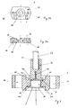
- one conventional more frequen tly used device (used by the applicant too) is shown in schematic section view in the fig. 1: it is made-up by a substantially cylindrical bush (BU); its lower side and hole (PA) hold the APD that ends superiorly with the plate of the glass window (VE).
- the monofiber cable (CA) with sheath (G) penetrates for a substantial depth (H) into the superior cylindrical part of the bush (BU) and continues into the inferior zone with a depth (h), without sheath with the sole uncovered fiber (FO).
- the fiber end (FO) is kept at a very little distance from the glass (VE); the cable (A) and its appendix (FO) are locked in the represented position filling all the inner bush volume (BU) with resin (preferably of black colour, in the high part and transparent in the lower one).
- the first object of the present invention is a system and relevant devices that do not show the above mentioned drawbacks and allow an efficient, sure and quick coupling - between the fiber and the photodetector.
- the system according to the invention for the alignment and the assembly of one optic fiber end with photodetector in hermetic package form with glass window and without fiber tail is characterized in that: one fiber end is ended by a semiconnector; it is prepared a support plate with two cylindrical concentric seats obtained on one of the major faces of this support; these concentric seats communicate between themselves by a common hole; the hermetic device of the photodetector is introduced into one of these seats keeping the glass window in a more internal position and matched on the hole; the free end of the semiconnector is introduced into the other seat, truing also the hole of the peeled fiber with the plate hole; and the said detector device and free semiconnector end are fixed to the relevant seats by synthetic catalyzed and possibly filled resins.
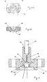
- the optic cable (CA) to be assembled to the APD is ended at the connection end with a semiconnector (1) (shown in enlarged scale in fig. 2) that is made-up by a body including (from the top to the bottom side) a cylindrical section (2C), having height (H2C) and inner diameter lightly higher than the external diameter (DCA) of the sheat; a truncated conical part or raiser (3TC) having height (H3TC) and diameter decreasing from (D2C) (substantial- l y equal to the sheath one) to the diameter (D4R) lightly higher than the fiber one (FO) (without sheath); a part (4R) having height (H4R) and inner diameter (D4R) lightly higher than the external one of the fiber (FO); a flanged lower part (5F) having height (H5F) and external diameter (D5F); and at last a recess (6SB) got in the lower face (9) of the body (1) of the
- the first operation consists in cleaning carefully the glass (VE) of APD, e.g. by isopropyl alcohol; for avoiding the halos produced by alcohol vaporisation, the glass (VE) must be accurately dried;
- the so resin-sheathed photodetector device is introduced into the support (S) (figures 3, 3A, or 4, 4A), that is substantially a plate (S) having a seat or superior zone (SF) for holding the assembled semiconductor (SC) of fig. 2, and one inferior seat (SI) (40) for holding the photodetector device (DF).
- the said seats (SF) and (SI) have both a shape of cylindrical and not very tall cavities.
- support (S) shows two symmetrical fastening holes (50) and (50') and at least a more little threaded hole (51).
- an epoxy resin is applied on the bottom (40) of the plate (S) for improving too the mechanical seal between APD (DF) and support (S).
- a light resin stratum (41) (indicated with the points in figure 3) is formed. This operation also can be made in mass-production on the devices to be assembled.
- the inferior face of the flanged semiconnector part (SC), and further the inferior face of the resin drop (RC) introduced into the recess (6SB) are inserted into the seat (30) of the support (S) plate, that, as the figures 3 and 4 show, is much more wide and tall than the flange (5F) of the semiconnector (SC).
- the flanged.cylinder part is placed into a clamp that is aligned for assuring the squareness between the axis of the said cylinder (1) and the plate reference plane.
- the lapped cylinder (9) surface is sent in ledge with the plate reference plane and, with sole traverse movements with reference to the fiber axis, it is possible to optimize the alignment between the active part of the device (DF) and the fiber (FO).
- the plate (S) and the cylinder (SC) are locked together by carbon-filled epoxy resin, batching e.g. 0.35 gr. of carbon for 1 gr. of resin (RA).
- an air stratum (AR) is applied between the fiber end (FO) in the recess (6SB) and the glass (VE) of the device instead of a resin stratum as it occurs into the jacket (I) of figure 1; this fact generates a Fresnel loss in optic connection (with respect to the former technique with resin applied between fiber and glass) of ab. 0.4 dB.
- the assembly has a good optic efficiency and perfect mechani- chal performances, using a wired and well-protected fiber. FUrther it is allowed the maximum flexibility in the selection of the connector and the photodiode type to be used.
Abstract
Description
- The present invention relates to a system for the connection between photodetector and optic fiber, in particular for the alignment and assembly of optic fibers with photodetectors in hermetic package with glass window and without fiber leader.
- It is well-known that the success of the transmission system by optic fiber used in communications is connected to the availability of solid state sources and detectors, that must be efficient, reliable and cheap, such as the one assembled in hermetic package without fiber leader, type APD (avalanche photo-diode), that require fiber-photodetector assembly having an high sturdiness and quality.
- It is known that the package tightness is indispensable for guaranteeing the protection from pollution produced by chip contamination agents that, owing to high input voltages amounting to ab. 200 V necessary for getting the avalanche gain, would reduce greatly the component life.
- The connection efficiency between fiber and APD through the glass window can be very high, as the APD construction technique allows to get good performances with a useful photosensitive area having a diameter comprised between 250 and 600 /um, to which corresponds a maximum distance of the fibre without connection losses comprised between 0.49 and 1.35 mm..
- The classic solutions for the connection of the fiber with a detector supplied with glass window and without leader are numerous but not free from drawbacks.
- To briefly illustrate the ideas, one conventional more frequen tly used device (used by the applicant too) is shown in schematic section view in the fig. 1: it is made-up by a substantially cylindrical bush (BU); its lower side and hole (PA) hold the APD that ends superiorly with the plate of the glass window (VE). The monofiber cable (CA) with sheath (G) penetrates for a substantial depth (H) into the superior cylindrical part of the bush (BU) and continues into the inferior zone with a depth (h), without sheath with the sole uncovered fiber (FO).
- Generally between the superior cylindrical part (BU') of the bush (BU) and the passage (PA) having an inferior diameter it is foreseen a truncated conical fitting (BU").
- As the drawing shows, the fiber end (FO) is kept at a very little distance from the glass (VE); the cable (A) and its appendix (FO) are locked in the represented position filling all the inner bush volume (BU) with resin (preferably of black colour, in the high part and transparent in the lower one).
- The line-up of the terminal fiber (FO) part with the lower APD was possibly by means of micromovements of the fiber. Among the more important drawbacks of this assembly type, the following ones can be mentioned:
- - the jacket (I) between the free lower fiber end (FO) and the lower surface of the glass (VE) holds a resin stratum that, in some conditions, damages and breaks the said glass (VE);
- - the jacket (I) height between (VE) and (FO) is notoriously critical as the maximum coupling is got in correspondance to a well-fixed value.
- The adjustment of (I) is not easy if we consider the device in question: in fact, if the free fiber end is pushed too much against (VE), the fiber is bended until its breackage; on the contrary, if it is too much far from (VE), the coupling losses increase.
- The first object of the present invention is a system and relevant devices that do not show the above mentioned drawbacks and allow an efficient, sure and quick coupling - between the fiber and the photodetector.
- The system according to the invention for the alignment and the assembly of one optic fiber end with photodetector in hermetic package form with glass window and without fiber tail is characterized in that: one fiber end is ended by a semiconnector; it is prepared a support plate with two cylindrical concentric seats obtained on one of the major faces of this support; these concentric seats communicate between themselves by a common hole; the hermetic device of the photodetector is introduced into one of these seats keeping the glass window in a more internal position and matched on the hole; the free end of the semiconnector is introduced into the other seat, truing also the hole of the peeled fiber with the plate hole; and the said detector device and free semiconnector end are fixed to the relevant seats by synthetic catalyzed and possibly filled resins.
- These and other objects and advantages of the invention will appear better in the following description of the embodiment forms (preferred and not limitative) shown in the annexed drawings, in which:
- - the figures 2,3,4 are schematic partially sectioned views of an optic fiber terminal and respectively of two assemblies of this terminal with two plates or bushes lightly different one from the other.
- - the figures 3A and 4A are plan views of bushes or plates for the assemblies of the figures 3 and 4;
- - the figures 3B and 4B are the traverse sections of the bushes shown in the figures 3A and 4A.
- Making reference to the figures from 2 to 4B, the system phases according to the present invention can be fixed as follows:
- According to a first object of the invention, the optic cable (CA) to be assembled to the APD is ended at the connection end with a semiconnector (1) (shown in enlarged scale in fig. 2) that is made-up by a body including (from the top to the bottom side) a cylindrical section (2C), having height (H2C) and inner diameter lightly higher than the external diameter (DCA) of the sheat; a truncated conical part or raiser (3TC) having height (H3TC) and diameter decreasing from (D2C) (substantial- ly equal to the sheath one) to the diameter (D4R) lightly higher than the fiber one (FO) (without sheath); a part (4R) having height (H4R) and inner diameter (D4R) lightly higher than the external one of the fiber (FO); a flanged lower part (5F) having height (H5F) and external diameter (D5F); and at last a recess (6SB) got in the lower face (9) of the body (1) of the sub-connector having height (H6SB) and diameter (D6SB). The connection between the cable (CA) and the bush is got as follows (see also the figures 3 and 4):
- 1) the cylindrical body (2C) (and partially the truncated cone section 3TC too) of the bush (1) is preferably filled with epoxy resin (e.g. of the EPOTEX 302 type);
- 2) the peeled fiber end (FO) is introduced into the bush (1) until the plastic external sheath (CA) is in ledge on the larger base (20) of the truncated cone section (3TC); generally the free end of FO crosses the recess (6SB);
- 3) an epoxy resin, charged with alumina (e.g. 0.27-0.37 gr. of alumina for 1 gr. of resin), is prepared and a drop of it is introduced into the recess or slot (6SB) of the bush (1) around the fiber hole (FO) in the component side;
- 4) the resin is polymerized, e.g. at room temperature for ab. 1 hour or at 60°C for ab. 15 minutes and so on;
- 5) when the polymerization is completed, it will be made the cylinder surface (9) lapping by a conventional technique. The figures 3 and 4 show the polymerized resin stratum applied during the phase 1) that is indicated with (RI) and the resin drop charged with (RC).
- 6) The first operation consists in cleaning carefully the glass (VE) of APD, e.g. by isopropyl alcohol; for avoiding the halos produced by alcohol vaporisation, the glass (VE) must be accurately dried;
- 7) then the metallic package of the device (APD) is cleaned and a resin stratum is applied around this one (conductive silver paste) shown with (RCC);
- 8) the so resin-sheathed photodetector device is introduced into the support (S) (figures 3, 3A, or 4, 4A), that is substantially a plate (S) having a seat or superior zone (SF) for holding the assembled semiconductor (SC) of fig. 2, and one inferior seat (SI) (40) for holding the photodetector device (DF).
- Preferably the said seats (SF) and (SI) have both a shape of cylindrical and not very tall cavities.
- Further the support (S) shows two symmetrical fastening holes (50) and (50') and at least a more little threaded hole (51).
- The superior hole or seat (SF) (30) has a step shape (30') (figures 3, 3A and 3B) or quite two steps (30 and 30") (figures 4, 4A and 4B).
- The step seat (30) is also accurately degreased before introducing the hermetic device (DF) into it.
- The glass (VE) of this last one must be in correspondance with the plate (S) reference plane.
- For making easier this operation, it can be used a ground punch, placed in ledge on the reference plane, sending the APD device in contact with the same tool (not shown).
- All the above described parts are placed into an oven e.g. at 60° C for ab. 18 hours.
- When the polymerization is over, an epoxy resin is applied on the bottom (40) of the plate (S) for improving too the mechanical seal between APD (DF) and support (S).
- A light resin stratum (41) (indicated with the points in figure 3) is formed. This operation also can be made in mass-production on the devices to be assembled.
- The inferior face of the flanged semiconnector part (SC), and further the inferior face of the resin drop (RC) introduced into the recess (6SB) are inserted into the seat (30) of the support (S) plate, that, as the figures 3 and 4 show, is much more wide and tall than the flange (5F) of the semiconnector (SC).
- For testing the optic output power of the fiber (FO) placed into the cylinder (1), it is used a proper adapter for the photodetector (not shown as it is well-known).
- After having placed the APD bushed device into the proper seat (DI) of the support plate (S), the flanged.cylinder part is placed into a clamp that is aligned for assuring the squareness between the axis of the said cylinder (1) and the plate reference plane.
- The lapped cylinder (9) surface is sent in ledge with the plate reference plane and, with sole traverse movements with reference to the fiber axis, it is possible to optimize the alignment between the active part of the device (DF) and the fiber (FO).
- The plate (S) and the cylinder (SC) are locked together by carbon-filled epoxy resin, batching e.g. 0.35 gr. of carbon for 1 gr. of resin (RA).
- It is got the resin stratum (RA).
- An advantage of this technique with respect to the former one consists in having a fiber introduced into a rigid body (SC), which is locked and sent into ledge on the bush plane (1): therefore it is eliminated the positioning in height of the fiber and this fact renders it more handy.
- Further the cylinder (1) with the introduced fiber (FO) is lapped, avoiding in this way the cut of the peeled fiber,
- as the cut must be controlled each time and often requires remakings due to the delicacy of the non-protected fiber. According to an advantageous feature of the invention, now an air stratum (AR) is applied between the fiber end (FO) in the recess (6SB) and the glass (VE) of the device instead of a resin stratum as it occurs into the jacket (I) of figure 1; this fact generates a Fresnel loss in optic connection (with respect to the former technique with resin applied between fiber and glass) of ab. 0.4 dB.
- The air stratum (AR) is minimum, therefore it can be noticed with a great difficulty in the figures 3 and 4.
- The components assembled with the conventional technique of fig. 1 and with the described system were tested for qualifying the process in environmental conditions that simulate the worse exercize conditions.
- It was obtained that the components assembled with the conventional process can suffer breakdowns, due to tightness loss produced by the mechanical stress generated by the resin on the window (VE) of ADP for the different thermal dilatation coefficients of used materials.
- For locating all components subject to this breackdown type, it is necessary to submit all production to a burn-in that shows the component degradation.
- This burn-in involves industrial costs, therefore it is surely advantageous and preferable to use the process according to the invention that does not show the above mentioned breackdown.
- The sole little drawback of this last process is a loss amount ing to ab. 0.4 dB, due to the reflection in the interface between glass and fiber, air and glass of the APD window.. The same process according to the invention is suitable for an industrial production as it requires assembly times without requiring further screening after the assembly.
- The assembly has a good optic efficiency and perfect mechani- chal performances, using a wired and well-protected fiber. FUrther it is allowed the maximum flexibility in the selection of the connector and the photodiode type to be used.
- The present invention was described with illustrative aims making reference to the preferred fulfilment forms, represented in the annexed drawings: it is obvious that they can be subject to variants, changes, replacements and similar ones that, being at disposal of the mean skilled technicial, undergo automatically in the field and spirit of the invention.
Claims (8)
Applications Claiming Priority (2)
| Application Number | Priority Date | Filing Date | Title |
|---|---|---|---|
| IT23587/83A IT1169922B (en) | 1983-11-04 | 1983-11-04 | SYSTEM AND DEVICES FOR CONNECTING DETECTORS AND FIBER OPTICS |
| IT2358783 | 1983-11-04 |
Publications (2)
| Publication Number | Publication Date |
|---|---|
| EP0183857A2 true EP0183857A2 (en) | 1986-06-11 |
| EP0183857A3 EP0183857A3 (en) | 1987-02-25 |
Family
ID=11208353
Family Applications (1)
| Application Number | Title | Priority Date | Filing Date |
|---|---|---|---|
| EP84112457A Withdrawn EP0183857A3 (en) | 1983-11-04 | 1984-10-16 | System and devices for the connection of photodetectors and optic fiber |
Country Status (7)
| Country | Link |
|---|---|
| US (1) | US4709979A (en) |
| EP (1) | EP0183857A3 (en) |
| BR (1) | BR8405599A (en) |
| ES (1) | ES8608183A1 (en) |
| IT (1) | IT1169922B (en) |
| MX (1) | MX157482A (en) |
| NO (1) | NO844307L (en) |
Cited By (4)
| Publication number | Priority date | Publication date | Assignee | Title |
|---|---|---|---|---|
| EP0304182A2 (en) * | 1987-08-19 | 1989-02-22 | Nortel Networks Corporation | Fibre tailed opto-electronic transducer |
| EP0446711A1 (en) * | 1990-03-13 | 1991-09-18 | Sumitomo Electric Industries, Ltd. | Optical module including receptacle, and method of producing the same |
| US5170453A (en) * | 1990-08-28 | 1992-12-08 | Sumitomo Electric Industries, Ltd. | Optical module |
| US5304818A (en) * | 1990-03-16 | 1994-04-19 | Sumitomo Electric Industries, Ltd. | Lead frame |
Families Citing this family (20)
| Publication number | Priority date | Publication date | Assignee | Title |
|---|---|---|---|---|
| GB8816603D0 (en) * | 1988-07-13 | 1988-08-17 | Bt & D Technologies Ltd | Optical components |
| US5119462A (en) * | 1990-01-29 | 1992-06-02 | 501 Nippon Sheet Glass Co., Ltd. | Photosemiconductor and optical fiber welded module |
| US5189716A (en) * | 1990-01-29 | 1993-02-23 | Nippon Sheet Glass Co., Ltd. | Photosemiconductor and optical fiber welded module |
| GB9217732D0 (en) * | 1992-08-20 | 1992-09-30 | Bt & D Technologies Ltd | Optical devices |
| JP3417505B2 (en) * | 1995-05-12 | 2003-06-16 | アイシン・エィ・ダブリュ株式会社 | Control device for automatic transmission |
| DE19803225C1 (en) | 1998-01-28 | 1999-08-19 | Litef Gmbh | Optical fiber connection with a light receiver |
| US6867377B2 (en) | 2000-12-26 | 2005-03-15 | Emcore Corporation | Apparatus and method of using flexible printed circuit board in optical transceiver device |
| US6905260B2 (en) | 2000-12-26 | 2005-06-14 | Emcore Corporation | Method and apparatus for coupling optical elements to optoelectronic devices for manufacturing optical transceiver modules |
| US6863444B2 (en) | 2000-12-26 | 2005-03-08 | Emcore Corporation | Housing and mounting structure |
| US6799902B2 (en) | 2000-12-26 | 2004-10-05 | Emcore Corporation | Optoelectronic mounting structure |
| US7021836B2 (en) * | 2000-12-26 | 2006-04-04 | Emcore Corporation | Attenuator and conditioner |
| US7215883B1 (en) | 2003-01-24 | 2007-05-08 | Jds Uniphase Corporation | Methods for determining the performance, status, and advanced failure of optical communication channels |
| US7002131B1 (en) | 2003-01-24 | 2006-02-21 | Jds Uniphase Corporation | Methods, systems and apparatus for measuring average received optical power |
| US6863453B2 (en) | 2003-01-28 | 2005-03-08 | Emcore Corporation | Method and apparatus for parallel optical transceiver module assembly |
| US7909776B2 (en) * | 2004-04-30 | 2011-03-22 | Roche Diagnostics Operations, Inc. | Lancets for bodily fluid sampling supplied on a tape |
| GB2428104B (en) * | 2005-07-07 | 2009-06-03 | Agilent Technologies Inc | Optoelectronic device |
| JP2009253166A (en) * | 2008-04-09 | 2009-10-29 | Yazaki Corp | Optical communication module |
| US7699539B2 (en) * | 2008-07-29 | 2010-04-20 | Comoss Electronic Co., Ltd. | Connector for plastic optical fiber |
| US20190129108A1 (en) * | 2017-10-31 | 2019-05-02 | Versalume LLC | Modular Laser Connector Packaging System and Method |
| US10551542B1 (en) | 2018-12-11 | 2020-02-04 | Corning Incorporated | Light modules and devices incorporating light modules |
Citations (3)
| Publication number | Priority date | Publication date | Assignee | Title |
|---|---|---|---|---|
| US4101197A (en) * | 1975-06-06 | 1978-07-18 | Plessey Handel Und Investments Ag | Connectors for coaxially coupling the end of a linear optical waveguide element for a receiving surface |
| GB2017963A (en) * | 1978-03-30 | 1979-10-10 | Amp Inc | Optical fibre/transducer coupling |
| GB2099605A (en) * | 1981-06-01 | 1982-12-08 | Raytheon Co | Fiber optic connector |
Family Cites Families (1)
| Publication number | Priority date | Publication date | Assignee | Title |
|---|---|---|---|---|
| JPS5522713A (en) * | 1978-08-04 | 1980-02-18 | Fujitsu Ltd | Connector mechanism of photo semiconductor device |
-
1983
- 1983-11-04 IT IT23587/83A patent/IT1169922B/en active
-
1984
- 1984-10-16 EP EP84112457A patent/EP0183857A3/en not_active Withdrawn
- 1984-10-22 US US06/663,240 patent/US4709979A/en not_active Expired - Fee Related
- 1984-10-26 MX MX203188A patent/MX157482A/en unknown
- 1984-10-30 NO NO844307A patent/NO844307L/en unknown
- 1984-10-31 ES ES537280A patent/ES8608183A1/en not_active Expired
- 1984-11-01 BR BR8405599A patent/BR8405599A/en not_active IP Right Cessation
Patent Citations (3)
| Publication number | Priority date | Publication date | Assignee | Title |
|---|---|---|---|---|
| US4101197A (en) * | 1975-06-06 | 1978-07-18 | Plessey Handel Und Investments Ag | Connectors for coaxially coupling the end of a linear optical waveguide element for a receiving surface |
| GB2017963A (en) * | 1978-03-30 | 1979-10-10 | Amp Inc | Optical fibre/transducer coupling |
| GB2099605A (en) * | 1981-06-01 | 1982-12-08 | Raytheon Co | Fiber optic connector |
Non-Patent Citations (1)
| Title |
|---|
| IEEE TRANSACTIONS ON COMPONENTS, HYBRIDS AND MANUFACTURING TECHNOLOGY, vol. CHMT-6, no. 3, September 1983, pages 334-342, New York, US; H.M. BERG et al.: "Optical coupling in fiber optics packages with surface emitting LED's" * |
Cited By (7)
| Publication number | Priority date | Publication date | Assignee | Title |
|---|---|---|---|---|
| EP0304182A2 (en) * | 1987-08-19 | 1989-02-22 | Nortel Networks Corporation | Fibre tailed opto-electronic transducer |
| EP0304182A3 (en) * | 1987-08-19 | 1989-11-15 | Stc Plc | Fibre tailed opto-electronic transducer |
| US4988159A (en) * | 1987-08-19 | 1991-01-29 | Stc Plc | Fiber tailed optoelectronic transducer |
| EP0446711A1 (en) * | 1990-03-13 | 1991-09-18 | Sumitomo Electric Industries, Ltd. | Optical module including receptacle, and method of producing the same |
| US5127071A (en) * | 1990-03-13 | 1992-06-30 | Sumitomo Electric Industries, Ltd. | Optical module including receptacle, and method of producing the same |
| US5304818A (en) * | 1990-03-16 | 1994-04-19 | Sumitomo Electric Industries, Ltd. | Lead frame |
| US5170453A (en) * | 1990-08-28 | 1992-12-08 | Sumitomo Electric Industries, Ltd. | Optical module |
Also Published As
| Publication number | Publication date |
|---|---|
| MX157482A (en) | 1988-11-24 |
| BR8405599A (en) | 1985-09-10 |
| ES537280A0 (en) | 1986-06-01 |
| US4709979A (en) | 1987-12-01 |
| ES8608183A1 (en) | 1986-06-01 |
| IT8323587A0 (en) | 1983-11-04 |
| EP0183857A3 (en) | 1987-02-25 |
| IT1169922B (en) | 1987-06-03 |
| NO844307L (en) | 1985-05-06 |
Similar Documents
| Publication | Publication Date | Title |
|---|---|---|
| EP0183857A2 (en) | System and devices for the connection of photodetectors and optic fiber | |
| US4222629A (en) | Fiber optic connector assembly | |
| US4186996A (en) | Optic adaptor junction | |
| US5586207A (en) | Methods and assemblies for packaging opto-electronic devices and for coupling optical fibers to the packaged devices | |
| KR100349598B1 (en) | Small form factor transceiver module using silicon optical bench | |
| US4708429A (en) | Optical fiber assembly and optically coupled device package including same | |
| US4186994A (en) | Arrangement for coupling between an electrooptic device and an optical fiber | |
| CN103650140B (en) | Wafer-class encapsulation platform for transceiver | |
| US4702556A (en) | Method of assembling a light emitting device with an optical fiber | |
| US5381494A (en) | Packaged optical devices | |
| US7153039B2 (en) | Connection of optical waveguides to optical devices | |
| US5692084A (en) | Package for an optoelectronic device | |
| US4386821A (en) | Opto-electronic coupling head and method for fitting such a head | |
| US5127074A (en) | Method of fabricating an optical package | |
| US5687270A (en) | Photodetector module capable of preventing deviation of optical axis | |
| CN110673279A (en) | Edge-coupled photoelectric device packaging structure and preparation method thereof | |
| GB2026235A (en) | Light emitting diode mounting structure for optical fiber communications | |
| US6526205B1 (en) | Method and apparatus for the passive alignment of optical components | |
| CN210605107U (en) | Edge coupling photoelectric device packaging structure | |
| US20020028050A1 (en) | Optical module | |
| US5522001A (en) | Optical fiber coupled devices and method of assembling same | |
| JPS59166906A (en) | Semiconductor laser coupling device | |
| US7093986B2 (en) | Low cost optical module | |
| US5276762A (en) | Magnetic holding methods for optical fiber I/O assembly | |
| US6999494B2 (en) | Packaging and passive alignment of microlens and molded receptacle |
Legal Events
| Date | Code | Title | Description |
|---|---|---|---|
| PUAI | Public reference made under article 153(3) epc to a published international application that has entered the european phase |
Free format text: ORIGINAL CODE: 0009012 |
|
| AK | Designated contracting states |
Kind code of ref document: A2 Designated state(s): AT BE CH DE FR GB LI NL SE |
|
| PUAL | Search report despatched |
Free format text: ORIGINAL CODE: 0009013 |
|
| AK | Designated contracting states |
Kind code of ref document: A3 Designated state(s): AT BE CH DE FR GB LI NL SE |
|
| 17P | Request for examination filed |
Effective date: 19870408 |
|
| 17Q | First examination report despatched |
Effective date: 19900808 |
|
| STAA | Information on the status of an ep patent application or granted ep patent |
Free format text: STATUS: THE APPLICATION IS DEEMED TO BE WITHDRAWN |
|
| 18D | Application deemed to be withdrawn |
Effective date: 19901219 |
|
| RIN1 | Information on inventor provided before grant (corrected) |
Inventor name: SPODATI, FABRIZIO Inventor name: TAMBURELLO, MARIO |