EP0182913B1 - Method of adjusting electronic circuits - Google Patents
Method of adjusting electronic circuits Download PDFInfo
- Publication number
- EP0182913B1 EP0182913B1 EP85902163A EP85902163A EP0182913B1 EP 0182913 B1 EP0182913 B1 EP 0182913B1 EP 85902163 A EP85902163 A EP 85902163A EP 85902163 A EP85902163 A EP 85902163A EP 0182913 B1 EP0182913 B1 EP 0182913B1
- Authority
- EP
- European Patent Office
- Prior art keywords
- electronic circuit
- melt
- adjusting
- cut
- circuit
- Prior art date
- Legal status (The legal status is an assumption and is not a legal conclusion. Google has not performed a legal analysis and makes no representation as to the accuracy of the status listed.)
- Expired - Lifetime
Links
Images

Classifications
-
- H—ELECTRICITY
- H03—ELECTRONIC CIRCUITRY
- H03H—IMPEDANCE NETWORKS, e.g. RESONANT CIRCUITS; RESONATORS
- H03H1/00—Constructional details of impedance networks whose electrical mode of operation is not specified or applicable to more than one type of network
-
- H—ELECTRICITY
- H04—ELECTRIC COMMUNICATION TECHNIQUE
- H04N—PICTORIAL COMMUNICATION, e.g. TELEVISION
- H04N17/00—Diagnosis, testing or measuring for television systems or their details
- H04N17/04—Diagnosis, testing or measuring for television systems or their details for receivers
Definitions
- This invention relates to a method for adjusting an electronic circuit used for a television receiver or the like when it is adjusted upon being manufactured.
- an electronic circuit for use in a television receiver and so on the characteristic thereof is normally changed and adjusted by finely adjusting the magnitude of a current flowing through such circuit. This is generally carried out by setting the electronic circuit in the driving (operating) mode and, in this state, rotating a semi-fixed resistor inserted into the circuit, the voltage and the like at a necessary operation point are adjusted so as to fall within a standardised value.
- US-A-3656115 and 4201970 disclose methods of trimming currents using fusible matrices corresponding to the precharacterising part of claim 1.
- This invention seeks to use fusible links to enable the semi-fixed resistor to be omitted to thereby improve the reliability of the electronic circuit after it was adjusted and also is to simplify the adjustment itself to thereby reduce the adjusting time.
- a method for adjusting an electronic circuit wherein the circuit includes at least one connection wire, connected in series or in parallel to an element inserted at a predetermined point of said electronic circuit and which can be melt-cut by flowing a current therethrough; characterised in that the electronic circuit is compensated for tolerances therein to set an operation state to a standardized value by detecting the operation state of said electronic circuit by a detector circuit and, on the basis of the detected result, it is judged whether said at least one connection wire is to be melt-cut or not and, if so, said detection circuit command at least one of said at least one connection wire to be melt-cut by automatic supply from adjustment means of said current through at least one of said connection wire thereby to adjust said electronic circuit.
- Figure 1 is a block diagram useful for explaining an embodiment of a method for adjusting an electronic circuit according to the present invention
- figure 2 is a cross-sectional view illustrating an example of an element used in the present invention
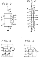
- figures 3, 4, 5 and 6 are cross-sectional views illustrating main parts of other embodiments of the present invention, respectively.
- reference numeral 1 designates a signal input terminal, 2 a preceding stage circuit, 3 a succeeding stage circuit and 4 a signal output terminal.
- a DC power source such as a drive power supply source and the like in the preceding stage circuit 2
- four resistors 11, 12, 13 and 14 are connected in series.
- the connection point between the resistors 12 and 13 is connected to a predetermined point of the preceding stage circuit 2.
- the resistors 12 and 13 become adjusting elements and the resistance values thereof are selected to be extremely low as compared with other resistors 11 and 14.
- respective resistance values R1, R2, R3 and R4 of the resistors 11, 12, 13 and 14 are 200K ⁇ , 200 ⁇ , 300 ⁇ and 300K ⁇ , respectively.
- An electronic circuit 10 is constructed as described above.
- the connection points among the respective resistors are denoted by P, Q and R, respectively.
- connection wires 17 and 18 are previously connected in parallel to the resistors 12 and 13 which become the adjusting elements, respectively.
- Fig. 2 illustrates an element 19 which incorporates therein the connection wires 17 and 18.
- the connection wires 17 and 18 are connected between one ends of three terminals 7, 8 and 9 made of conductive material and this portion is molded by a mold material 20 such as resin and so on.
- a mold material 20 such as resin and so on.
- connection wires 17 and 18 there can be used such one which can easliy be melt-cut by the current flowed thereto.
- such a connection wire is suitable which can easily be melt-cut by a current of 2A (about 0.6V) for a time period of 2m sec.
- a detector circuit 5 As shown in Fig. 1, there are prepared a detector circuit 5 and an adjusting circuit 6. A measuring terminal (electrode) of the detector circuit 5 is connected to a necessary point to be measured (the connection point between the preceding stage circuit 2 and the succeeding stage circuit 3, in this embodiment) of the electronic circuit 10 and lead wires from the adjusting circuit 6 are respectively connected to the aforesaid points P, Q and R.
- the electronic circuit 10 is set in the driving (operating) state and the operating state (characteristic and the like) of the electronic circuit 10 is checked by the detector circuit 5. If the electronic circuit is in its normal operating state, the connection wires 17 and 18 are not melt-cut but are left as they are. Therefore, at that time, the resistors 12 and 13 are in the short-circuited state, respectively.
- connection wire 17 is melt-cut.
- both the resistors 12 and 13 are used is better, it is enough to melt-cut both the connection wires 17 and 18.
- While the supply of the current from the adjusting circuit 6 may be manually carried out on the basis of the detected result by the detector circuit 5, it may be possible that the supply of the current is automatically carried out by controlling the adjusting circuit 6 on the basis of a command signal issued from the detector circuit 5.
- the semi-fixed resistor tends to easily vary its resistance value due to the invasion of dusts, water and so on or because it has a movable portion, according to the method of the present invention, since such semi-fixed resistor is not required, even after it was adjusted, the resistance value thereof is not changed, thus increasing the reliability by that much.
- Fig. 3 illustrates other embodiment of the present invention.
- the resistor 13 as the adjusting element is connected in series to the connection wire 18
- other circuit elements are connected in the same way as those of Fig. 1.
- the respective resistance values R1, R2, R3 and R4 of the resistors 11, 12, 13 and 14 are selected to be 50K ⁇ ,270 ⁇ , 33K ⁇ and 4.7K ⁇ , respectively.
- the resistor 12 under the illustrated state, the resistor 12 is short-circuited and the resistors 14 and 13 are connected in parallel to each other, so that the resistance value between the points P and Q is zero and that the resistance value between the points Q and R is 4114 ⁇ which is slightly lower than 4700 ⁇ . If under such state either the connection wire 17 or 18 or both of them are melt-cut the respective resistance values to the ground side and to the opposite side from the point Q can be adjusted finely.
- Fig. 4 shows a further embodiment of the present invention.
- two routes are provided for the P-Q-R path and the above mentioned connection wires 17 and 18 are interposed in the routes, in which the two routes are both used or either of them is used, selectively.
- Fig. 5 shows a further embodiment in which capacitors 22 and 23 as the adjusting elements are connected in parallel to a capacitor 21 via the connection wires 17 and 18.
- the capacity value can be adjusted by melt-cutting the connection wires 17 and 18 in the manner similar to the above.
- Fig. 6 shows a further embodiment in which coils 25 and 26 as the adjusting elements are connected in parallel to a coil 24 via the connection wires 17 and 18. Also in Fig. 6, the inductance value can be adjusted by melt-cutting the connection wires 17 and 18 similarly as described above.
- connection wire used for the interconnection of a semiconductor
- the adjusting element is provided in parallel to this bonding wire, they are molded integrally and terminals are led out from one and another ends of the molded member.
- connecting wires 17 and 18 are molded by the mold material, of course, they may be connected discretely.
- Reference numeral 5 represents the detector circuit, 6 the adjusting circuit, 10 the electronic circuit, 12 and 13 the adjusting elements, respectively, 17 and 18 the connection wires, respectively and 19 the element.
Landscapes
- Engineering & Computer Science (AREA)
- Health & Medical Sciences (AREA)
- Biomedical Technology (AREA)
- General Health & Medical Sciences (AREA)
- Multimedia (AREA)
- Signal Processing (AREA)
- Apparatuses And Processes For Manufacturing Resistors (AREA)
- Testing, Inspecting, Measuring Of Stereoscopic Televisions And Televisions (AREA)
- Electric Clocks (AREA)
- Filters And Equalizers (AREA)
- Details Of Television Systems (AREA)
- Semiconductor Integrated Circuits (AREA)
- Thermistors And Varistors (AREA)
- Oscillators With Electromechanical Resonators (AREA)
Abstract
Description
- This invention relates to a method for adjusting an electronic circuit used for a television receiver or the like when it is adjusted upon being manufactured.
- In an electronic circuit for use in a television receiver and so on, the characteristic thereof is normally changed and adjusted by finely adjusting the magnitude of a current flowing through such circuit. This is generally carried out by setting the electronic circuit in the driving (operating) mode and, in this state, rotating a semi-fixed resistor inserted into the circuit, the voltage and the like at a necessary operation point are adjusted so as to fall within a standardised value.
- According to this method, since the scattering of the characteristics of the semi-fixed resistor itself is large, even if the adjusting angle of the semi-fixed resistor is determined, the characteristics of all the electronic circuits cannot always fall within the standardised values. For this reason, the rotational adjustment must be carried out in each electronic circuit, requiring a relatively long time of about 20 seconds for one adjustment. Further, since the semi-fixed resistor is of a so-called moveable type, after the adjustment, the rotational angle may be changed due to the vibration, contact and so on. Accordingly, upon transportation and the like thereof, care has to be taken that this semi-fixed resistor is not disturbed, etc.
- US-A-3656115 and 4201970 disclose methods of trimming currents using fusible matrices corresponding to the precharacterising part of claim 1.
- This invention seeks to use fusible links to enable the semi-fixed resistor to be omitted to thereby improve the reliability of the electronic circuit after it was adjusted and also is to simplify the adjustment itself to thereby reduce the adjusting time.
- According to the present invention, there is provided a method for adjusting an electronic circuit wherein the circuit includes at least one connection wire, connected in series or in parallel to an element inserted at a predetermined point of said electronic circuit and which can be melt-cut by flowing a current therethrough; characterised in that the electronic circuit is compensated for tolerances therein to set an operation state to a standardized value by detecting the operation state of said electronic circuit by a detector circuit and, on the basis of the detected result, it is judged whether said at least one connection wire is to be melt-cut or not and, if so, said detection circuit command at least one of said at least one connection wire to be melt-cut by automatic supply from adjustment means of said current through at least one of said connection wire thereby to adjust said electronic circuit.
- The invention will be further described by way of non-limitative example with reference to the accompanying drawings, in which:-
- Figure 1 is a block diagram useful for explaining an embodiment of a method for adjusting an electronic circuit according to the present invention, figure 2 is a cross-sectional view illustrating an example of an element used in the present invention, and figures 3, 4, 5 and 6 are cross-sectional views illustrating main parts of other embodiments of the present invention, respectively.
- An embodiment of a method for adjusting an electronic circuit according to the present invention will hereinafter be described with reference to the drawings.
- In Fig. 1, reference numeral 1 designates a signal input terminal, 2 a preceding stage circuit, 3 a succeeding stage circuit and 4 a signal output terminal. To a DC power source such as a drive power supply source and the like in the preceding stage circuit 2, four
resistors resistors resistors other resistors 11 and 14. By way of example, respective resistance values R₁, R₂, R₃ and R₄ of theresistors -
Connection wires resistors element 19 which incorporates therein theconnection wires connection wires terminals 7, 8 and 9 made of conductive material and this portion is molded by amold material 20 such as resin and so on. As theconnection wires connection wires - Turning back to Fig. 1, the
terminals 7, 8 and 9 of the above mentionedelement 19 are previously connected (soldered) to the aforesaid points P, Q and R of the electronic circuit 10, respectively. After the adjustment which will be described later, they are not removed. Accordingly, on a printed circuit board, thiselement 19 is mounted together with other electronic parts, too. - Next, the adjusting method will be described. As shown in Fig. 1, there are prepared a
detector circuit 5 and an adjusting circuit 6. A measuring terminal (electrode) of thedetector circuit 5 is connected to a necessary point to be measured (the connection point between the preceding stage circuit 2 and the succeedingstage circuit 3, in this embodiment) of the electronic circuit 10 and lead wires from the adjusting circuit 6 are respectively connected to the aforesaid points P, Q and R. - Then, the electronic circuit 10 is set in the driving (operating) state and the operating state (characteristic and the like) of the electronic circuit 10 is checked by the
detector circuit 5. If the electronic circuit is in its normal operating state, theconnection wires resistors - If under this operation state such a result is obtained by making the resistance value at the ground side from the point Q be slightly larger, a current is supplied to the
connection wire 18 from the adjusting circuit 6 to thereby melt-cut this connection wire. In the case reverse to the above, it is enough that theconnection wire 17 is melt-cut. Alternatively, if such a result that both theresistors connection wires - While the supply of the current from the adjusting circuit 6 may be manually carried out on the basis of the detected result by the
detector circuit 5, it may be possible that the supply of the current is automatically carried out by controlling the adjusting circuit 6 on the basis of a command signal issued from thedetector circuit 5. - Even when the prior art semi-fixed resistor is used, since the practical variable range of the resistance value is very small as compared with the whole resistance value (the resistance value between the point Q and the ground in Fig. 1), if the resistance values of the respective resistors are set to be satisfactory values, the satisfactory adjustment can be brought about by either of the connection and disconnection of the connection wires as seen in the above mentioned example.
- According to the present invention as set forth above, since under the operation state of the electronic circuit 10 the
necessary connection wire detector circuit 5, it is possible to carry out the adjustment of the so-called electronic circuit very easily and for an extremely short time of period (several milli seconds). Accordingly, even when the adjusting operation is carried out in each electronic circuit 10, it hardly takes a long time of period for such adjustment. Further, although the semi-fixed resistor tends to easily vary its resistance value due to the invasion of dusts, water and so on or because it has a movable portion, according to the method of the present invention, since such semi-fixed resistor is not required, even after it was adjusted, the resistance value thereof is not changed, thus increasing the reliability by that much. - Fig. 3 illustrates other embodiment of the present invention. In this embodiment, except for the fact that the
resistor 13 as the adjusting element is connected in series to theconnection wire 18, other circuit elements are connected in the same way as those of Fig. 1. The respective resistance values R₁, R₂, R₃ and R₄ of theresistors resistor 12 is short-circuited and theresistors connection wire - Fig. 4 shows a further embodiment of the present invention. In this embodiment, two routes are provided for the P-Q-R path and the above mentioned
connection wires - Fig. 5 shows a further embodiment in which
capacitors capacitor 21 via theconnection wires connection wires - Fig. 6 shows a further embodiment in which coils 25 and 26 as the adjusting elements are connected in parallel to a
coil 24 via theconnection wires connection wires - While in the above mentioned embodiments the adjusting elements and the connection wires therefor are independently provided, such a version may be possible that a bonding wire used for the interconnection of a semiconductor is used as the connection wire, the adjusting element is provided in parallel to this bonding wire, they are molded integrally and terminals are led out from one and another ends of the molded member. While the above mentioned connecting
wires -
Reference numeral 5 represents the detector circuit, 6 the adjusting circuit, 10 the electronic circuit, 12 and 13 the adjusting elements, respectively, 17 and 18 the connection wires, respectively and 19 the element.
Claims (7)
- A method for adjusting an electronic circuit (10) wherein the circuit includes at least one connection wire (17, 18), connected in series or in parallel to an element inserted at a predetermined point (P, Q, R) of said electronic circuit and which can be melt-cut by flowing a current therethrough; characterised in that the electronic circuit (10) is compensated for tolerances therein to set an operation state to a standardized value by detecting the operation state of said electronic circuit by a detector circuit (5) and, on the basis of the detected result, it is judged whether said at least one connection wire (17, 18) is to be melt-cut or not and, if so, said detection circuit (5) command at least one of said at least one connection wire to be melt-cut by automatic supply from adjustment means (6) of said current through at least one of said connection wire thereby to adjust said electronic circuit.
- A method of producing a plurality of electronic circuits having a standardized operation state, characterized by applying to each circuit the method of claim 1.
- A method for compensating an electronic circuit according to claim 1 or 2, characterised in that said adjusting element comprises at least one resistor element (R1-R4).
- A method for compensating an electronic circuit according to claim 1 or 2, characterised in that said adjusting element comprises at least one capacitor element (21, 22, 23).
- A method for compensating an electronic circuit according to claim 1 or 2, characterised in that said adjusting element comprises at least one inductor element (24, 25, 26).
- A method for compensating an electronic circuit according to any preceding claim, wherein the circuit includes a housing element (19) which houses said at least one connection wire (17, 18) to be melt-cut by flowing a current therethrough.
- A method for compensating an electronic circuit according to claim 6, characterised in that said housing element includes three terminals (7, 8, 9).
Priority Applications (1)
| Application Number | Priority Date | Filing Date | Title |
|---|---|---|---|
| AT85902163T ATE98825T1 (en) | 1984-05-10 | 1985-05-09 | PROCEDURE FOR ADJUSTING ELECTRONIC CIRCUITS. |
Applications Claiming Priority (2)
| Application Number | Priority Date | Filing Date | Title |
|---|---|---|---|
| JP93729/84 | 1984-05-10 | ||
| JP59093729A JPS60236585A (en) | 1984-05-10 | 1984-05-10 | Control method of electronic circuit |
Publications (3)
| Publication Number | Publication Date |
|---|---|
| EP0182913A1 EP0182913A1 (en) | 1986-06-04 |
| EP0182913A4 EP0182913A4 (en) | 1988-01-28 |
| EP0182913B1 true EP0182913B1 (en) | 1993-12-15 |
Family
ID=14090496
Family Applications (1)
| Application Number | Title | Priority Date | Filing Date |
|---|---|---|---|
| EP85902163A Expired - Lifetime EP0182913B1 (en) | 1984-05-10 | 1985-05-09 | Method of adjusting electronic circuits |
Country Status (7)
| Country | Link |
|---|---|
| US (1) | US4689550A (en) |
| EP (1) | EP0182913B1 (en) |
| JP (1) | JPS60236585A (en) |
| KR (1) | KR860700191A (en) |
| AT (1) | ATE98825T1 (en) |
| DE (1) | DE3587686T2 (en) |
| WO (1) | WO1985005510A1 (en) |
Families Citing this family (11)
| Publication number | Priority date | Publication date | Assignee | Title |
|---|---|---|---|---|
| JP2577897B2 (en) * | 1986-10-31 | 1997-02-05 | 日本テキサス・インスツルメンツ 株式会社 | Constant voltage power supply circuit |
| US4978904A (en) * | 1987-12-15 | 1990-12-18 | Gazelle Microcircuits, Inc. | Circuit for generating reference voltage and reference current |
| US4970415A (en) * | 1989-07-18 | 1990-11-13 | Gazelle Microcircuits, Inc. | Circuit for generating reference voltages and reference currents |
| JP2601933B2 (en) * | 1990-04-13 | 1997-04-23 | 株式会社東芝 | Solid-state imaging device |
| US5780918A (en) * | 1990-05-22 | 1998-07-14 | Seiko Epson Corporation | Semiconductor integrated circuit device having a programmable adjusting element in the form of a fuse mounted on a margin of the device and a method of manufacturing the same |
| JPH04373148A (en) * | 1991-06-21 | 1992-12-25 | Nippon Steel Corp | Fuse structure of semiconductor device |
| US5410186A (en) * | 1991-12-19 | 1995-04-25 | International Business Machines Company | Programmable digital to analog converter |
| US5367202A (en) * | 1992-11-06 | 1994-11-22 | National Semiconductor Corporation | Voltage reference ladder having improved linearity |
| JPH10135756A (en) * | 1996-10-31 | 1998-05-22 | Mitsumi Electric Co Ltd | Adjustment method of circuit characteristics in circuit body |
| JP3398564B2 (en) * | 1997-04-11 | 2003-04-21 | 富士通株式会社 | Semiconductor device |
| US6822345B2 (en) * | 2002-04-09 | 2004-11-23 | Sun Microsystems, Inc. | Chip/package resonance damping using controlled package series resistance |
Family Cites Families (7)
| Publication number | Priority date | Publication date | Assignee | Title |
|---|---|---|---|---|
| US3656115A (en) * | 1971-04-19 | 1972-04-11 | Bunker Ramo | Fusible link matrix for programmable networks |
| DE2256688B2 (en) * | 1972-11-18 | 1976-05-06 | Robert Bosch Gmbh, 7000 Stuttgart | PROCESS FOR SEPARATING CONDUCTOR TRACKS ON INTEGRATED CIRCUITS |
| US4016483A (en) * | 1974-06-27 | 1977-04-05 | Rudin Marvin B | Microminiature integrated circuit impedance device including weighted elements and contactless switching means for fixing the impedance at a preselected value |
| JPS529850A (en) * | 1975-07-15 | 1977-01-25 | Oki Electric Ind Co Ltd | Semiifixed electron variable resistor |
| US4150366A (en) * | 1976-09-01 | 1979-04-17 | Motorola, Inc. | Trim network for monolithic circuits and use in trimming a d/a converter |
| US4201970A (en) * | 1978-08-07 | 1980-05-06 | Rca Corporation | Method and apparatus for trimming resistors |
| US4412241A (en) * | 1980-11-21 | 1983-10-25 | National Semiconductor Corporation | Multiple trim structure |
-
1984
- 1984-05-10 JP JP59093729A patent/JPS60236585A/en active Pending
-
1985
- 1985-05-09 AT AT85902163T patent/ATE98825T1/en not_active IP Right Cessation
- 1985-05-09 KR KR1019850700416A patent/KR860700191A/en not_active Ceased
- 1985-05-09 DE DE85902163T patent/DE3587686T2/en not_active Expired - Fee Related
- 1985-05-09 WO PCT/JP1985/000261 patent/WO1985005510A1/en not_active Ceased
- 1985-05-09 EP EP85902163A patent/EP0182913B1/en not_active Expired - Lifetime
- 1985-05-09 US US06/822,303 patent/US4689550A/en not_active Expired - Lifetime
Also Published As
| Publication number | Publication date |
|---|---|
| JPS60236585A (en) | 1985-11-25 |
| EP0182913A1 (en) | 1986-06-04 |
| US4689550A (en) | 1987-08-25 |
| ATE98825T1 (en) | 1994-01-15 |
| KR860700191A (en) | 1986-03-31 |
| EP0182913A4 (en) | 1988-01-28 |
| DE3587686T2 (en) | 1994-04-07 |
| WO1985005510A1 (en) | 1985-12-05 |
| DE3587686D1 (en) | 1994-01-27 |
Similar Documents
| Publication | Publication Date | Title |
|---|---|---|
| US4689550A (en) | Method for adjusting an electronic circuit | |
| US4338646A (en) | Current limiting circuit | |
| WO1996018109A9 (en) | An integrated resistor for sensing electrical parameters | |
| US4713602A (en) | Circuit resistance adjusting device | |
| US3300689A (en) | Voltage sensing circuit | |
| US4794269A (en) | Load controller for automobile | |
| JP3814019B2 (en) | Fusing circuit for semiconductor IC | |
| EP0273425B1 (en) | Filter circuit | |
| US4797578A (en) | Arrangement for adjusting an impedance network in an integrated semiconductor circuit | |
| US4316135A (en) | Circuit arrangement for feeding modules in user stations | |
| US4771184A (en) | Electronic switch apparatus | |
| US6717416B2 (en) | Circuit configuration for the voltage supply of a two-wire sensor | |
| EP0167884A2 (en) | DC supply unit with overcurrent protection | |
| EP0401911A1 (en) | Switching device | |
| US5378998A (en) | Current measurement circuits | |
| US4803472A (en) | Phase signal detecting device | |
| CA2097448C (en) | Signal separation circuit | |
| JPH08106331A (en) | Power source controller | |
| US5199406A (en) | Igniter for an internal combustion engine | |
| US7318081B2 (en) | Band-pass filter and tracking signal processor circuit | |
| JP2752432B2 (en) | Current sensor and current detection method using the same | |
| US5418488A (en) | Device for establishing a current in an analog part of an integrated logic and analog circuit | |
| JPH0716177B2 (en) | Optical transmitter circuit | |
| JPS62105522A (en) | Driving device for switching element | |
| JPS63308410A (en) | Optical sensor for two-terminal network |
Legal Events
| Date | Code | Title | Description |
|---|---|---|---|
| PUAI | Public reference made under article 153(3) epc to a published international application that has entered the european phase |
Free format text: ORIGINAL CODE: 0009012 |
|
| 17P | Request for examination filed |
Effective date: 19860102 |
|
| AK | Designated contracting states |
Kind code of ref document: A1 Designated state(s): AT DE FR GB IT NL |
|
| A4 | Supplementary search report drawn up and despatched |
Effective date: 19880128 |
|
| 17Q | First examination report despatched |
Effective date: 19891208 |
|
| GRAA | (expected) grant |
Free format text: ORIGINAL CODE: 0009210 |
|
| AK | Designated contracting states |
Kind code of ref document: B1 Designated state(s): AT DE FR GB IT NL |
|
| REF | Corresponds to: |
Ref document number: 98825 Country of ref document: AT Date of ref document: 19940115 Kind code of ref document: T |
|
| REF | Corresponds to: |
Ref document number: 3587686 Country of ref document: DE Date of ref document: 19940127 |
|
| ITF | It: translation for a ep patent filed | ||
| ET | Fr: translation filed | ||
| ITTA | It: last paid annual fee | ||
| PLBE | No opposition filed within time limit |
Free format text: ORIGINAL CODE: 0009261 |
|
| STAA | Information on the status of an ep patent application or granted ep patent |
Free format text: STATUS: NO OPPOSITION FILED WITHIN TIME LIMIT |
|
| 26N | No opposition filed | ||
| PGFP | Annual fee paid to national office [announced via postgrant information from national office to epo] |
Ref country code: DE Payment date: 20010430 Year of fee payment: 17 |
|
| PGFP | Annual fee paid to national office [announced via postgrant information from national office to epo] |
Ref country code: GB Payment date: 20010509 Year of fee payment: 17 |
|
| PGFP | Annual fee paid to national office [announced via postgrant information from national office to epo] |
Ref country code: AT Payment date: 20010514 Year of fee payment: 17 |
|
| PGFP | Annual fee paid to national office [announced via postgrant information from national office to epo] |
Ref country code: FR Payment date: 20010518 Year of fee payment: 17 |
|
| PGFP | Annual fee paid to national office [announced via postgrant information from national office to epo] |
Ref country code: NL Payment date: 20010531 Year of fee payment: 17 |
|
| REG | Reference to a national code |
Ref country code: GB Ref legal event code: IF02 |
|
| PG25 | Lapsed in a contracting state [announced via postgrant information from national office to epo] |
Ref country code: GB Free format text: LAPSE BECAUSE OF NON-PAYMENT OF DUE FEES Effective date: 20020509 Ref country code: AT Free format text: LAPSE BECAUSE OF NON-PAYMENT OF DUE FEES Effective date: 20020509 |
|
| PG25 | Lapsed in a contracting state [announced via postgrant information from national office to epo] |
Ref country code: NL Free format text: LAPSE BECAUSE OF NON-PAYMENT OF DUE FEES Effective date: 20021201 |
|
| PG25 | Lapsed in a contracting state [announced via postgrant information from national office to epo] |
Ref country code: DE Free format text: LAPSE BECAUSE OF NON-PAYMENT OF DUE FEES Effective date: 20021203 |
|
| GBPC | Gb: european patent ceased through non-payment of renewal fee |
Effective date: 20020509 |
|
| PG25 | Lapsed in a contracting state [announced via postgrant information from national office to epo] |
Ref country code: FR Free format text: LAPSE BECAUSE OF NON-PAYMENT OF DUE FEES Effective date: 20030131 |
|
| NLV4 | Nl: lapsed or anulled due to non-payment of the annual fee |
Effective date: 20021201 |
|
| REG | Reference to a national code |
Ref country code: FR Ref legal event code: ST |