EP0182490A1 - Improvements in or relating to stepping motor driven electronic timepieces - Google Patents
Improvements in or relating to stepping motor driven electronic timepieces Download PDFInfo
- Publication number
- EP0182490A1 EP0182490A1 EP85307295A EP85307295A EP0182490A1 EP 0182490 A1 EP0182490 A1 EP 0182490A1 EP 85307295 A EP85307295 A EP 85307295A EP 85307295 A EP85307295 A EP 85307295A EP 0182490 A1 EP0182490 A1 EP 0182490A1
- Authority
- EP
- European Patent Office
- Prior art keywords
- switching means
- coil
- impedance element
- signals
- rotor
- Prior art date
- Legal status (The legal status is an assumption and is not a legal conclusion. Google has not performed a legal analysis and makes no representation as to the accuracy of the status listed.)
- Granted
Links
Images


Classifications
-
- H—ELECTRICITY
- H02—GENERATION; CONVERSION OR DISTRIBUTION OF ELECTRIC POWER
- H02P—CONTROL OR REGULATION OF ELECTRIC MOTORS, ELECTRIC GENERATORS OR DYNAMO-ELECTRIC CONVERTERS; CONTROLLING TRANSFORMERS, REACTORS OR CHOKE COILS
- H02P8/00—Arrangements for controlling dynamo-electric motors rotating step by step
- H02P8/02—Arrangements for controlling dynamo-electric motors rotating step by step specially adapted for single-phase or bi-pole stepper motors, e.g. watch-motors, clock-motors
-
- G—PHYSICS
- G04—HOROLOGY
- G04C—ELECTROMECHANICAL CLOCKS OR WATCHES
- G04C3/00—Electromechanical clocks or watches independent of other time-pieces and in which the movement is maintained by electric means
- G04C3/14—Electromechanical clocks or watches independent of other time-pieces and in which the movement is maintained by electric means incorporating a stepping motor
- G04C3/143—Means to reduce power consumption by reducing pulse width or amplitude and related problems, e.g. detection of unwanted or missing step
Definitions
- This invention relates to timepiece turn detecting circuits and, although it is not so restricted, it is more particularly concerned with the turn detector circuit usually provided in electronic wristwatches and other so-called electronic timepieces - that is to say with the means provided in such timepieces for detecting whether or not the stepping motor has responded correctly with a stepping turn when a driving pulse has been applied to its excitation coil.
- a method for driving a turn detector circuit for detecting whether or not a driving pulse applied to the coil of a timepiece stepping motor having a rotor and a stator causes said rotor to rotate correctly said turn detection being effected by connecting a high impedance element electrically to said coil upon operation of first switching means and connecting a low impedance element electrically to said coil upon operation of second switching means aftemately characterised by the steps of applying first signals to said first switching means, applying second signals to said second switching means and then applying third signals to said second switching means for disconnecting said low impedance element from said coil while said high impedance element is connected thereto at the time of turn detection.
- the said first and second signals are applied alternately to said second switching means.
- the said low impedance element and said high impedance element are respectively a low ohmic resistance element and a high ohmic resistance element.
- the invention also comprises a timepiece stepping motor having a rotor,'a stator, a coil, and a turn detector circuit for detecting whether a driving pulse applied to the coil causes said rotor to rotate correctly, said turn detection being effected by connecting a high impedance element of said circuit electrically to said coil upon operation of first switching means and connecting a low impedance element of said circuit electrically to said coil upon operation of second switching means alternately characterised in that in operation the circuit applies first signals to said first switching means, second signals to said second switching means and then third signals to said second switching means for disconnecting said low impedance element from said coil while said high impedance element is connected thereto at the time of turn detection.
- the circuit of Figure 1 is known per se as is the stepping motor of Figure 2, and the timing chart of Figure 3 shows the known method of operating the circuit of Figure 1.
- This known method will now be described.
- a drive pulse is applied to an excitation coil 9 of the motor, a transistor device Tr1 (actually a p-type MOSFET) and a transistor device Tr6 (actually an n-type MOSFET) are rendered conductive, and an electric current flows from a power supply source (not shown) through a path indicated by a broken line 14.
- 12 and 13 are high impedance elements and may be high ohmic resistances.
- Tr6 remains conductive but further MOSFETS Tr2 and Tr3 are rendered conductive and non-conductive alternately. Tr2 and Tr6, when conductive, constitute low impedance elements. As will now be seen, closed loops indicated by broken lines 15 and 16 are alternately established, and a voltage VRS is induced in the coil due to the motion of rotor 17. This voltage is represented in Figure 3 as the voltage appearing at point 4.
- the voltage VRS is usually about 2.0 volts (flowing into the source, not shown, of the power supply voltage VDD via a parasitic diode in an integrated circuit and is clamped to a forward voltage of VDD + the drop in the parasitic diode), with VSS being set at 0 volts, but, if the rotor does not rotate correctly, VRS is usually between 0.3 and 1.2 volts.
- the difference between the two possible values of VRS (the higher value if the rotor turns correctly and the lower value if it does not) is detected by comparators 10 and 11, and in this way turn detection, i.e. detection of whether or not the rotor has turned cor- rectty in response to a driving pulse, is effected.
- the voltage VRS is not solely dependent upon whether or not the rotor turns correctly in response to a driving pulse but is affected by many other features including the details of shape and material of the rotor 17 and the stator 18, the inductance and resistance of the motor coil 9, the resistances or impedances of the elements 12 and 13, the timing of the switching of Tr2 and Tr6, the stray capacitances at the ends 4 and 8 of the coil 9, and the switching timing T2.
- the variation of the voltage VRS due to such extraneous causes as the foregoing can cause erroneous turn detection to occur, the rotor often being detected as not turning when it actually is turning, or being detected as turning when in fact it is not. This is a serious defect causing increase in the consumption of electrical power by the watch or causing the watch to become slow.
- the switching timings of Tr2 and Tr3 and of Tr6 and Tr7 during the time T2 are so selected that Tr3 or Tr7 is rendered conductive just when Tr2 or Tr6 is rendered non-conductive (see Figure 4A).
- the switching timing is intended to be selected as just mentioned, small amounts of time delay occur due to wiring capacitance and gate capacitance in an integrated circuit.
- the signals applied to the gates of Tr2 and Tr3 are delayed by the same amount, or if the signal applied to Tr2 is delayed more than the signal applied to Tr3 (as shown in Figure 4C).
- the present invention seeks to avoid the foregoing defects and to provide a method of driving a turn detection circuit which will obviate or at least greatly reduce the liability to erroneous turn detection.
- This object is achieved, in accordance with the present invention, by so operating the circuit that the timing at which Tr2 or Tr6 is rendered non-conductive is made to differ, logically, from the timing at which Tr3 or Tr7 is rendered conductive, so that Tr2 and Tr3 will not be simultaneously non-conductive and neither will Tr6 and Tr7.
- the method of driving the turn detector circuit includes the steps of applying a first signal to a first switching means (for connecting said high impedance element to said coil), applying a second signal to a second switching means (for connecting said low impedance element to said coil) and then applying a third signal to the second switching means for disconnecting the low impedance element from said coil.
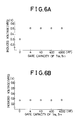
- Figure 6A shows VRS in volts (V) as ordinates against the gate capacitance in piezo-farads (pF) of Tr3 or Tr7 when the known method hereinbefore described is used, i.e. with the conventional logic in which Tr2 and Tr3 or Tr6 and Tr7 are alternately rendered conductive and non-conductive as in Figure 3.
- the voltage VRS suddenly increases at a point where, as a result of increase in the gate capacitance of Tr3 or Tr7 a certain amount of increased delay occurs.
- Figure 6B which similarly shows the voltage VRS when the gate capacitance of Tr3 or Tr7 is increased when using the method of this invention, i.e.
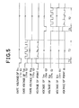
- Tr3 or Tr7 is maintained conductive throughout the time T2 for switching Tr2 or Tr6 as shown in Figure 5.
- the value of the voltage VRS remains sensibly constant overthewhole range of plotted gate capacitance of Tr3 or Tr7.
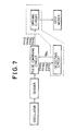
- Figure 7 is a block circuit diagram of an electronic timepiece for producing the time chart waveforms shown in Figure 5.
- a pulse combining circuit PCC provides the gate voltage V TrIG for Tr1, the gate voltage V Tr2G for Tr2, the gate voltage V TrSG for Tr5 and the gate voltage V Tr6G for Tr6 during the time T1 and provides the gate voltage V-rric for Tr1, the gate voltage V Tr2G for Tr 2, the gate voltage V Tr3 for Tr3, the gate voltage V Tr5 for Tr5, the gate voltage V Tr6 for Tr6 and the gate voltage V Tr7 for Tr7 during the time T2.
- the detecting and driving circuit itself is as in Figure 1 but, as will now be appreciated it is operated in accordance with the method of this invention which is quite different from the known conventional method.
- the oscillator is the usual time base oscillator of an electronic wristwatch and feeds into the usual divider.
- the great advantage of the method of the present invention is that, because the voltage VRS remains stable, the liability to erroneous turn detection is greatly reduced. Delays due to wiring capacitance or gate capacitance do not cause erroneous detection through timing delays. This is a great advantage from the standpoint of the designer and manufacturer producing integrated circuits embodying watch circuitry for if the method of the present invention is employed, the designer of an integrated circuit in which the circuit of Figure 1 is incorporated does not have to pay close attention to the gate capacitances of Tr2, Tr6, Tr3 or Tr7 or to delays introduced by elements leading up to the gates of these devices and, hence, there is no need to control or check such items during manufacturing the integrated circuits.
Landscapes
- Engineering & Computer Science (AREA)
- Power Engineering (AREA)
- Physics & Mathematics (AREA)
- General Physics & Mathematics (AREA)
- Electromechanical Clocks (AREA)
- Control Of Stepping Motors (AREA)
Abstract
Description
- This invention relates to timepiece turn detecting circuits and, although it is not so restricted, it is more particularly concerned with the turn detector circuit usually provided in electronic wristwatches and other so-called electronic timepieces - that is to say with the means provided in such timepieces for detecting whether or not the stepping motor has responded correctly with a stepping turn when a driving pulse has been applied to its excitation coil.
- In U.S. Specification No. 4,326,278 there is disclosed a method for driving a turn detector circuit for detecting whether or not a driving pulse applied to the coil of a timepiece stepping motor having a rotor and a stator causes said rotor to rotate correctly, said turn detection being effected by connecting a high impedance element electrically to said coil upon operation of first switching means and connecting a low impedance element electrically to said coil upon operation of second switching means alternately.
- However, the voltage induced in the motor coil is not solely dependent upon whether or not the rotor turns correctly in response to a driving pulse but is affected by many other features. According, therefore, to the present invention there is provided a method for driving a turn detector circuit for detecting whether or not a driving pulse applied to the coil of a timepiece stepping motor having a rotor and a stator causes said rotor to rotate correctly, said turn detection being effected by connecting a high impedance element electrically to said coil upon operation of first switching means and connecting a low impedance element electrically to said coil upon operation of second switching means aftemately characterised by the steps of applying first signals to said first switching means, applying second signals to said second switching means and then applying third signals to said second switching means for disconnecting said low impedance element from said coil while said high impedance element is connected thereto at the time of turn detection.
- Preferably, the said first and second signals are applied alternately to said second switching means.
- Preferably, the said low impedance element and said high impedance element are respectively a low ohmic resistance element and a high ohmic resistance element.
- The invention also comprises a timepiece stepping motor having a rotor,'a stator, a coil, and a turn detector circuit for detecting whether a driving pulse applied to the coil causes said rotor to rotate correctly, said turn detection being effected by connecting a high impedance element of said circuit electrically to said coil upon operation of first switching means and connecting a low impedance element of said circuit electrically to said coil upon operation of second switching means alternately characterised in that in operation the circuit applies first signals to said first switching means, second signals to said second switching means and then third signals to said second switching means for disconnecting said low impedance element from said coil while said high impedance element is connected thereto at the time of turn detection.
- The invention is illustrated, merely by way of example, in the accompanying drawings, in which:-
- Figure 1 shows a stepping motor driving circuit and turn detecting circuit for the stepping motor of a wristwatch;
- Figure 2 is a simplified schematic representation of a typical stepping motor as commonly used in a wristwatch,
- Figure 3 is a timing chart showing how the circuit of Figure 1 is operated in accordance with the methods of present day known practice;
- Figures 4A, 48, 4C and 4D are diagrams which explain the change in VRS (voltage induced in the motor coil due to motion of its rotor) caused by the deviation of switching timing during a time T2 for turn detection;
- Figure 5 is a timing chart showing how the circuit of Figure 1 is operated in accordance with the method of the present invention;
- Figures 6A and 68 are diagrams showing, respectively, results experimentally obtained when using the known conventional driving method for the turn detector circuit and the results experimentally obtained when using the driving method of the present invention; and
- Figure 7 is a block circuit diagram of an electronic timepiece including means for producing the timing chart waveforms shown in Figure 5.
- The circuit of Figure 1 is known per se as is the stepping motor of Figure 2, and the timing chart of Figure 3 shows the known method of operating the circuit of Figure 1. This known method will now be described. In this method when, at a time T1, a drive pulse is applied to an
excitation coil 9 of the motor, a transistor device Tr1 (actually a p-type MOSFET) and a transistor device Tr6 (actually an n-type MOSFET) are rendered conductive, and an electric current flows from a power supply source (not shown) through a path indicated by abroken line 14. 12 and 13 are high impedance elements and may be high ohmic resistances. At a time T2 when turn detection is to be effected, Tr6 remains conductive but further MOSFETS Tr2 and Tr3 are rendered conductive and non-conductive alternately. Tr2 and Tr6, when conductive, constitute low impedance elements. As will now be seen, closed loops indicated bybroken lines rotor 17. This voltage is represented in Figure 3 as the voltage appearing atpoint 4. If the rotor turns correctly in response to the driving pulse, the voltage VRS is usually about 2.0 volts (flowing into the source, not shown, of the power supply voltage VDD via a parasitic diode in an integrated circuit and is clamped to a forward voltage of VDD + the drop in the parasitic diode), with VSS being set at 0 volts, but, if the rotor does not rotate correctly, VRS is usually between 0.3 and 1.2 volts. The difference between the two possible values of VRS (the higher value if the rotor turns correctly and the lower value if it does not) is detected bycomparators - The above known method for driving a turn detector circuit to detect whether a stepping motor rotor turns or not will be found exemplified in U.S. Patent No. 4,326,278 issued April 20, 1982 to Shida et al.
- However, the voltage VRS is not solely dependent upon whether or not the rotor turns correctly in response to a driving pulse but is affected by many other features including the details of shape and material of the
rotor 17 and thestator 18, the inductance and resistance of themotor coil 9, the resistances or impedances of theelements ends coil 9, and the switching timing T2. The variation of the voltage VRS due to such extraneous causes as the foregoing can cause erroneous turn detection to occur, the rotor often being detected as not turning when it actually is turning, or being detected as turning when in fact it is not. This is a serious defect causing increase in the consumption of electrical power by the watch or causing the watch to become slow. - The modem trend towards small, compact wristwatches and the consequent use of stepping motors with very small rotors, stators, and coils has made extraneously caused variations in VRS particularly prone to occur and, in very small compact timepieces, bad time-keeping (the watch becoming slow) caused by the turn detection circuit responding as though the rotor is turning when in fact it is not, can be seriously troublesome.
- In the above described known method of driving the turn detection circuit, the switching timings of Tr2 and Tr3 and of Tr6 and Tr7 during the time T2 are so selected that Tr3 or Tr7 is rendered conductive just when Tr2 or Tr6 is rendered non-conductive (see Figure 4A). However, even though the switching timing is intended to be selected as just mentioned, small amounts of time delay occur due to wiring capacitance and gate capacitance in an integrated circuit. There are no problems if the signals applied to the gates of Tr2 and Tr3 are delayed by the same amount, or if the signal applied to Tr2 is delayed more than the signal applied to Tr3 (as shown in Figure 4C). However, a large value of voltage VRS will be induced if the signal applied to Tr3 is delayed more than the signal applied to Tr2 (as shown in Figure 48), for at the time T3 of Figure 4B when both the Tr2 and Tr3 are rendered non-conductive, there is no closed loop formed, and a high voltage VRS is accordingly induced.
- The present invention seeks to avoid the foregoing defects and to provide a method of driving a turn detection circuit which will obviate or at least greatly reduce the liability to erroneous turn detection. This object is achieved, in accordance with the present invention, by so operating the circuit that the timing at which Tr2 or Tr6 is rendered non-conductive is made to differ, logically, from the timing at which Tr3 or Tr7 is rendered conductive, so that Tr2 and Tr3 will not be simultaneously non-conductive and neither will Tr6 and Tr7.
- In the case of the present invention, the method of driving the turn detector circuit includes the steps of applying a first signal to a first switching means (for connecting said high impedance element to said coil), applying a second signal to a second switching means (for connecting said low impedance element to said coil) and then applying a third signal to the second switching means for disconnecting the low impedance element from said coil.
- The improvement obtained by use of the method of the present invention in place of the conventional known method will be seen from Figures 6A and 6B which show results experimentally obtained when using the old method - as shown in Figure 6A - and the results obtained when using the method of the present invention -as shown in Figure 6B.
- Figure 6A shows VRS in volts (V) as ordinates against the gate capacitance in piezo-farads (pF) of Tr3 or Tr7 when the known method hereinbefore described is used, i.e. with the conventional logic in which Tr2 and Tr3 or Tr6 and Tr7 are alternately rendered conductive and non-conductive as in Figure 3. As will be seen from Figure 6A the voltage VRS suddenly increases at a point where, as a result of increase in the gate capacitance of Tr3 or Tr7 a certain amount of increased delay occurs. Compare Figure 6A with Figure 6B which similarly shows the voltage VRS when the gate capacitance of Tr3 or Tr7 is increased when using the method of this invention, i.e. with the logic in which Tr3 or Tr7 is maintained conductive throughout the time T2 for switching Tr2 or Tr6 as shown in Figure 5. As will be seen from Figure 6B the value of the voltage VRS remains sensibly constant overthewhole range of plotted gate capacitance of Tr3 or Tr7.
- Figure 7 is a block circuit diagram of an electronic timepiece for producing the time chart waveforms shown in Figure 5.
- Referring to Figure 7, a pulse combining circuit PCC provides the gate voltage VTrIG for Tr1, the gate voltage VTr2G for Tr2, the gate voltage VTrSG for Tr5 and the gate voltage VTr6G for Tr6 during the time T1 and provides the gate voltage V-rric for Tr1, the gate voltage VTr2G for
Tr 2, the gate voltage V Tr3 for Tr3, the gate voltage VTr5for Tr5, the gate voltage VTr6for Tr6 and the gate voltage VTr7for Tr7 during the time T2. The detecting and driving circuit itself is as in Figure 1 but, as will now be appreciated it is operated in accordance with the method of this invention which is quite different from the known conventional method. The oscillator is the usual time base oscillator of an electronic wristwatch and feeds into the usual divider. - The great advantage of the method of the present invention is that, because the voltage VRS remains stable, the liability to erroneous turn detection is greatly reduced. Delays due to wiring capacitance or gate capacitance do not cause erroneous detection through timing delays. This is a great advantage from the standpoint of the designer and manufacturer producing integrated circuits embodying watch circuitry for if the method of the present invention is employed, the designer of an integrated circuit in which the circuit of Figure 1 is incorporated does not have to pay close attention to the gate capacitances of Tr2, Tr6, Tr3 or Tr7 or to delays introduced by elements leading up to the gates of these devices and, hence, there is no need to control or check such items during manufacturing the integrated circuits.
Claims (6)
Applications Claiming Priority (2)
| Application Number | Priority Date | Filing Date | Title |
|---|---|---|---|
| JP59216581A JPH0681551B2 (en) | 1984-10-16 | 1984-10-16 | Rotation detection method for step motor |
| JP216581/84 | 1984-10-16 |
Publications (2)
| Publication Number | Publication Date |
|---|---|
| EP0182490A1 true EP0182490A1 (en) | 1986-05-28 |
| EP0182490B1 EP0182490B1 (en) | 1988-09-07 |
Family
ID=16690656
Family Applications (1)
| Application Number | Title | Priority Date | Filing Date |
|---|---|---|---|
| EP85307295A Expired EP0182490B1 (en) | 1984-10-16 | 1985-10-11 | Improvements in or relating to stepping motor driven electronic timepieces |
Country Status (6)
| Country | Link |
|---|---|
| US (1) | US4673857A (en) |
| EP (1) | EP0182490B1 (en) |
| JP (1) | JPH0681551B2 (en) |
| DE (1) | DE3564875D1 (en) |
| HK (1) | HK71990A (en) |
| SG (1) | SG62689G (en) |
Families Citing this family (7)
| Publication number | Priority date | Publication date | Assignee | Title |
|---|---|---|---|---|
| JPH0823245B2 (en) * | 1991-11-12 | 1996-03-06 | 小松ウオール工業株式会社 | Sliding door device |
| JP3365250B2 (en) * | 1997-04-28 | 2003-01-08 | 関西日本電気株式会社 | Stepping motor drive |
| JPH11311651A (en) * | 1998-04-28 | 1999-11-09 | Mikuni Corp | Failure determination device for electromagnetic coil operation device |
| JP4652610B2 (en) * | 2001-05-30 | 2011-03-16 | セイコーインスツル株式会社 | Step motor rotation control device |
| DE10225610B4 (en) * | 2002-06-07 | 2006-12-28 | Trinamic Motion Control Gmbh & Co. Kg | Method and circuit arrangement for operating a stepper motor |
| JP2015061467A (en) * | 2013-09-20 | 2015-03-30 | カシオ計算機株式会社 | Stepping motor and clock |
| JP7545308B2 (en) * | 2020-12-08 | 2024-09-04 | シチズン時計株式会社 | Electronic clock |
Citations (2)
| Publication number | Priority date | Publication date | Assignee | Title |
|---|---|---|---|---|
| EP0062273A1 (en) * | 1981-03-31 | 1982-10-13 | Omega SA | Method of controlling a stepping motor |
| EP0097350A1 (en) * | 1982-06-21 | 1984-01-04 | Omega SA | Method of feeding a single phase stepping motor of a time piece |
Family Cites Families (4)
| Publication number | Priority date | Publication date | Assignee | Title |
|---|---|---|---|---|
| JPS5477164A (en) * | 1977-12-02 | 1979-06-20 | Seiko Instr & Electronics Ltd | Electronic watch |
| JPS5515054A (en) * | 1978-07-19 | 1980-02-01 | Seiko Instr & Electronics Ltd | Electronic watch |
| US4321521A (en) * | 1978-12-25 | 1982-03-23 | Kabushiki Kaisha Daini Seikosha | Detection device of electronic timepiece |
| JPS55147381A (en) * | 1979-05-04 | 1980-11-17 | Seiko Instr & Electronics Ltd | Detector for electronic watch |
-
1984
- 1984-10-16 JP JP59216581A patent/JPH0681551B2/en not_active Expired - Lifetime
-
1985
- 1985-10-04 US US06/784,240 patent/US4673857A/en not_active Expired - Lifetime
- 1985-10-11 DE DE8585307295T patent/DE3564875D1/en not_active Expired
- 1985-10-11 EP EP85307295A patent/EP0182490B1/en not_active Expired
-
1989
- 1989-09-11 SG SG626/89A patent/SG62689G/en unknown
-
1990
- 1990-09-13 HK HK719/90A patent/HK71990A/en active IP Right Revival
Patent Citations (2)
| Publication number | Priority date | Publication date | Assignee | Title |
|---|---|---|---|---|
| EP0062273A1 (en) * | 1981-03-31 | 1982-10-13 | Omega SA | Method of controlling a stepping motor |
| EP0097350A1 (en) * | 1982-06-21 | 1984-01-04 | Omega SA | Method of feeding a single phase stepping motor of a time piece |
Also Published As
| Publication number | Publication date |
|---|---|
| EP0182490B1 (en) | 1988-09-07 |
| DE3564875D1 (en) | 1988-10-13 |
| JPS6194598A (en) | 1986-05-13 |
| HK71990A (en) | 1990-09-21 |
| US4673857A (en) | 1987-06-16 |
| SG62689G (en) | 1990-01-26 |
| JPH0681551B2 (en) | 1994-10-12 |
Similar Documents
| Publication | Publication Date | Title |
|---|---|---|
| US7606116B2 (en) | Analogue electronic clock and motor control circuit | |
| US5712533A (en) | Power supply circuit for an electroluminescent lamp | |
| US4460282A (en) | Timepiece stepping motor drive circuit with stepping failure compensation | |
| EP0182490B1 (en) | Improvements in or relating to stepping motor driven electronic timepieces | |
| JPS6156792B2 (en) | ||
| US4158287A (en) | Driver circuit for electro-mechanical transducer | |
| US4321521A (en) | Detection device of electronic timepiece | |
| US4533257A (en) | Analog electric timepiece | |
| US4209971A (en) | Electronic timepiece | |
| CN102832867A (en) | Single-phase brushless motor drive circuit | |
| US4352172A (en) | Detection device of electronic timepiece | |
| US4204397A (en) | Electronic timepiece | |
| US4217751A (en) | Electronic timepiece | |
| CN102832866A (en) | Single-phase brushless motor drive circuit | |
| US4688948A (en) | Electronic analogue timepiece of DC magnetic field detection type | |
| US3806781A (en) | Electric oscillation maintenance circuit for motor element oscillations | |
| JPS5869500A (en) | Method of reducing power consumption of step motor and device for executing same method | |
| JPS60260883A (en) | Analog electronic timepiece | |
| GB2067795A (en) | Improvements in or Relating to Stepping Motor Driven Electronic Timepieces | |
| JPH0799796A (en) | Driving device for stepping motor | |
| US4518906A (en) | Driving device of stepping motor | |
| JPH10300870A (en) | Electronic clock | |
| JPS6373181A (en) | Apparatus for detecting driving of motor in electronic timepiece | |
| US4218652A (en) | Apparatus for measuring the intensity and direction of external magnetic fields including power supply and recording units having respective semi-conductor devices | |
| JPS609751Y2 (en) | electronic clock |
Legal Events
| Date | Code | Title | Description |
|---|---|---|---|
| PUAI | Public reference made under article 153(3) epc to a published international application that has entered the european phase |
Free format text: ORIGINAL CODE: 0009012 |
|
| AK | Designated contracting states |
Kind code of ref document: A1 Designated state(s): CH DE FR GB LI |
|
| 17P | Request for examination filed |
Effective date: 19860924 |
|
| RAP1 | Party data changed (applicant data changed or rights of an application transferred) |
Owner name: SEIKO INSTRUMENTS INC. |
|
| 17Q | First examination report despatched |
Effective date: 19871210 |
|
| GRAA | (expected) grant |
Free format text: ORIGINAL CODE: 0009210 |
|
| AK | Designated contracting states |
Kind code of ref document: B1 Designated state(s): CH DE FR GB LI |
|
| REF | Corresponds to: |
Ref document number: 3564875 Country of ref document: DE Date of ref document: 19881013 |
|
| ET | Fr: translation filed | ||
| REG | Reference to a national code |
Ref country code: CH Ref legal event code: PFA Free format text: SEIKO INSTRUMENTS INC. |
|
| PLBE | No opposition filed within time limit |
Free format text: ORIGINAL CODE: 0009261 |
|
| STAA | Information on the status of an ep patent application or granted ep patent |
Free format text: STATUS: NO OPPOSITION FILED WITHIN TIME LIMIT |
|
| 26N | No opposition filed | ||
| REG | Reference to a national code |
Ref country code: GB Ref legal event code: 746 Effective date: 19930902 |
|
| REG | Reference to a national code |
Ref country code: FR Ref legal event code: DL |
|
| REG | Reference to a national code |
Ref country code: GB Ref legal event code: IF02 |
|
| PGFP | Annual fee paid to national office [announced via postgrant information from national office to epo] |
Ref country code: GB Payment date: 20041006 Year of fee payment: 20 |
|
| PGFP | Annual fee paid to national office [announced via postgrant information from national office to epo] |
Ref country code: DE Payment date: 20041007 Year of fee payment: 20 |
|
| PGFP | Annual fee paid to national office [announced via postgrant information from national office to epo] |
Ref country code: FR Payment date: 20041008 Year of fee payment: 20 |
|
| PGFP | Annual fee paid to national office [announced via postgrant information from national office to epo] |
Ref country code: CH Payment date: 20041015 Year of fee payment: 20 |
|
| PG25 | Lapsed in a contracting state [announced via postgrant information from national office to epo] |
Ref country code: GB Free format text: LAPSE BECAUSE OF EXPIRATION OF PROTECTION Effective date: 20051010 |
|
| REG | Reference to a national code |
Ref country code: GB Ref legal event code: PE20 |
|
| REG | Reference to a national code |
Ref country code: CH Ref legal event code: PL |