EP0181126B1 - Signal synthesiser - Google Patents
Signal synthesiser Download PDFInfo
- Publication number
- EP0181126B1 EP0181126B1 EP85307700A EP85307700A EP0181126B1 EP 0181126 B1 EP0181126 B1 EP 0181126B1 EP 85307700 A EP85307700 A EP 85307700A EP 85307700 A EP85307700 A EP 85307700A EP 0181126 B1 EP0181126 B1 EP 0181126B1
- Authority
- EP
- European Patent Office
- Prior art keywords
- envelope
- signal
- circuit
- synthesiser
- pulse
- Prior art date
- Legal status (The legal status is an assumption and is not a legal conclusion. Google has not performed a legal analysis and makes no representation as to the accuracy of the status listed.)
- Expired
Links
- 230000000630 rising effect Effects 0.000 claims description 4
- 230000010363 phase shift Effects 0.000 claims description 2
- 239000003990 capacitor Substances 0.000 description 10
- 230000009977 dual effect Effects 0.000 description 5
- 238000002592 echocardiography Methods 0.000 description 2
- 238000010586 diagram Methods 0.000 description 1
- 238000007599 discharging Methods 0.000 description 1
- 238000001914 filtration Methods 0.000 description 1
- 238000000034 method Methods 0.000 description 1
- 230000004048 modification Effects 0.000 description 1
- 238000012986 modification Methods 0.000 description 1
- 238000002360 preparation method Methods 0.000 description 1
- 238000004088 simulation Methods 0.000 description 1
- 230000007704 transition Effects 0.000 description 1
Images

Classifications
-
- G—PHYSICS
- G01—MEASURING; TESTING
- G01H—MEASUREMENT OF MECHANICAL VIBRATIONS OR ULTRASONIC, SONIC OR INFRASONIC WAVES
- G01H3/00—Measuring characteristics of vibrations by using a detector in a fluid
- G01H3/005—Testing or calibrating of detectors covered by the subgroups of G01H3/00
-
- G—PHYSICS
- G01—MEASURING; TESTING
- G01S—RADIO DIRECTION-FINDING; RADIO NAVIGATION; DETERMINING DISTANCE OR VELOCITY BY USE OF RADIO WAVES; LOCATING OR PRESENCE-DETECTING BY USE OF THE REFLECTION OR RERADIATION OF RADIO WAVES; ANALOGOUS ARRANGEMENTS USING OTHER WAVES
- G01S7/00—Details of systems according to groups G01S13/00, G01S15/00, G01S17/00
- G01S7/52—Details of systems according to groups G01S13/00, G01S15/00, G01S17/00 of systems according to group G01S15/00
- G01S7/52004—Means for monitoring or calibrating
-
- H—ELECTRICITY
- H03—ELECTRONIC CIRCUITRY
- H03K—PULSE TECHNIQUE
- H03K17/00—Electronic switching or gating, i.e. not by contact-making and –breaking
- H03K17/16—Modifications for eliminating interference voltages or currents
Definitions
- This invention relates to a signal synthesiser for producing pulses simulating the characteristics of echo pulses generated during ultrasonic scanning techniques. Such pulses can then be used for calibration of equipment for processing the outputs of ultrasonic transducers.
- a signal synthesiser comprising means for generating a high frequency pulse train, means for producing an envelope having a rising edge, a falling edge and a plateau between those edges, means for selectively varying the rise and fall times of said edges of the envelope, means for varying the duration of the envelope, means for multiplying said envelope with, on the one hand, said high frequency pulse train and with, on the other hand, a substantially zero amplitude signal to provide two outputs having superimposed feed through components introduced by the multiplying means, and means for combining the output signals to derive a calibration signal substantially free of said feedthrough components.
- Preferably means is provided for effecting phase shift of said pulse train with respect to the envelope.
- the multiplying means employed in the present invention may be a dual matched multiplier such as the AD539 device manufactured by Analogue Devices. By using the device as indicated above, it is possible to achieve accurate multiplication involving high frequency signals while freeing the calibration signal from feedthrough components without any filtering.
- Means may be provided for varying the amplitude of the calibration signal, for example by means of a switched attenuator connected to the output of the combining means.
- the combining means may be a differential amplifier for effecting subtraction of one multiplied output from the other.
- a fixed frequency 20 MHz oscillator 10 is connected to a counter 12 which, in conjunction with a shift register 14, serves to produce four 5 MHz outputs 16 which are phase shifted by 90° with respect to one another. Any one of the outputs 16 may be selected by phase selection circuitry 18, e.g. manually operable switches located on a control console, and coupled to a dual multiplier (see Figure 1B) via buffer amplifier 20, analogue switching circuitry 22 (e.g. FET switches) and buffer/low pass filter section 24 which blocks frequencies exceeding 5 MHz.
- phase selection circuitry e.g. manually operable switches located on a control console
- analogue switching circuitry 22 e.g. FET switches
- buffer/low pass filter section 24 which blocks frequencies exceeding 5 MHz.
- the output of the counter 12 is connected to a divider chain 26 which provides a gating pulse on line 28 which may define a gating period and three pulse trains on lines 30, the pulse trains being different subdivisions of the gating pulse, e.g. so that there are 1, 2 or 4 pulses respectively within the gating interval (see the waveforms of Figures 2A, B, C and D).
- Figure 2A represents the gating pulses and it will be noted that the other three waveforms are multiples of this.
- the pulse trains on lines 30 govern whether the calibration signals produced will simulate a single echo or a multiple echo response, i.e. 1, 2 or 4 echoes in the example illustrated.
- Circuitry 32 which may comprise a number of manually operable switches for routing the signal on a selected one of the lines 30 to circuitry 34 for controlling generation of the envelope of the simulated pulses.
- Figures 2E, 2F and 2G illustrate the waveforms that may be applied to the circuit 34, according to the selection made.
- the control circuitry 34 also receives inputs from circuits 36, 38 and 40 which determines other parameters of the pulse envelope, namely envelope duration (circuit 36), pulse rise time (circuit 38) and pulse fall time (circuit 40).
- the circuits 36, 38 and 40 each include manually settable switching means for effecting adjustment of the respective parameters.
- the circuit 32 may also be used for controlling the relative timing of the simulated echo pulses in relation to the leading edge of the gating pulses, i.e. so as to simulate echos returned from targets at different positions.
- the leading edges of the pulse trains on lines 30 subdivide the gating pulse ( Figure 2A) into one, two or four and consequently the leading edges of the echo pulser provide seven timing increments with respect to the leading edges of the gating pulses.
- the pulse timing facility may be divorced from the single/multi-echo selection circuit 32.
- the envelope control circuit 34 includes a capacitor charging and discharging of which governs the rise and fall times of the envelope.
- the circuits 38, 40 may include a number of resistors (or resistor combinations) which can be selectively coupled to the capacitor to vary the CR time constant of charge or discharge and thereby adjust the rise and fall time of the envelope.
- the circuit 36 serves to produce a timing pulse whose duration determines the duration of the plateau of the envelope, as will be explained further below.
- the output side of the capacitor is connected to the dual multiplier ( Figure 1B) via buffer section 44, operation of the analogue switching section 22 being controlled by the envelope control section so that the switches are closed only for the duration of the envelope.
- the envelope signal produced at the output of circuit 34 is coupled to a comparator section 46 which is also coupled to a potentiometer circuit 48.
- the circuit 48 enables the amplitude of the envelope to be set to a selected fixed value.
- the capacitor is coupled to a selected resistor or resistor combination associated with circuit 40 so that the capacitor proceeds to discharge with a preset time constant.
- the falling voltage level is compared by circuit 46 with a zero reference level and when the latter level is reached, the comparator section 46 produces an output to reset the envelope control circuit in preparation for the next cycle of envelope generation.
- the envelope generated and supplied to the multiplier must not go negative. This is ensured by buffer 44.
- the envelope will be seen to comprise a rising edge 50, a falling edge 52 and a constant amplitude plateau 54.
- the rising and falling edges are of an exponential nature, they may be substantially linear if only a minor part of the exponential curves associated with the capacitor (and resistor combination) are utilised.
- the transition points 56 will in general be of a discontinuous nature and are therefore potential sources of high frequency components during subsequent handling by the multiplier.
- Figure 2M illustrates the wave form of the 5 MHz signal and it will be understood that this will be confined to a time interval corresponding to the duration of the envelope, i.e. by virtue of a control signal applied to the switching section via line 60. This is indicated by the waveform as depicted at 21 which illustrates the envelope of the 5 MHz signal without showing the fine detail of the high frequency signal.
- the signals on lines 62, 64 are applied to the dual matched multiplier 66 which is constituted by the circuit component AD539 manufactured by Analogue Devices.
- This device has two sets of multiplier inputs, i.e. 68, 70 and 72, 74 and outputs 76, 78.
- the outputs 76, 78 provide the products of the signals applied to the inputs 68, 70 and to the inputs 72, 74 respectively.
- a feature of the AD539 device is that it is capable of accurately multiplying signals of up to 60 MHz with signals of up to 5 MHz.
- the inputs 68 and 72 serve to handle signals up to 60 MHz while inputs 70 and 74 handle signals of up to 5 MHz.
- the envelope signals are applied to inputs 70 and 74, the 5 MHz carrier signal is applied to the input 68 and the input 72 is connected to the ground plane.
- the envelope (Figure 2H) includes discontinuities 56 which can give rise to significant and undesirable high frequency feedthrough components during multiplication. This is offset to some extent by the fact that the inputs 70 and 74 can handle signals up to 5 MHz-nevertheless such undesirable feedthrough components can occur even with the AD539 device. Advantage is therefore taken of the fact that this device is a dual matched multiplier by performing two multiplications, i.e. the desired multiplication and a multiplication of the envelope with a zero level signal. The latter multiplication will also suffer from feedthrough and can therefore be used to compensate the desired product signal by subtraction in circuit 80, e.g. a differential amplifier. This is illustrated by the waveform of Figures 2J and 2L.
- Figure 2J represents the product signal at output 76 from which it will be seen that unwanted feedthrough components 82 are present. Likewise in the case of the product signal at output 78-see Figure 2K. After subtraction however, the resulting output is substantially freed of the feedthrough components-see Figure 2L.
- the waveform of Figure 2L will be used as an echo simulating calibration pulse and that various parameters thereof can be readily varied, e.g. pulse duration, rise time, fall time and timing relative to the gating pulses.
- the phase relationship between the envelope and the carrier may be varied.
Landscapes
- Engineering & Computer Science (AREA)
- Physics & Mathematics (AREA)
- General Physics & Mathematics (AREA)
- Computer Networks & Wireless Communication (AREA)
- Radar, Positioning & Navigation (AREA)
- Remote Sensing (AREA)
- Measurement Of Velocity Or Position Using Acoustic Or Ultrasonic Waves (AREA)
- Ultra Sonic Daignosis Equipment (AREA)
Description
- This invention relates to a signal synthesiser for producing pulses simulating the characteristics of echo pulses generated during ultrasonic scanning techniques. Such pulses can then be used for calibration of equipment for processing the outputs of ultrasonic transducers.
- According to the present invention there is provided a signal synthesiser comprising means for generating a high frequency pulse train, means for producing an envelope having a rising edge, a falling edge and a plateau between those edges, means for selectively varying the rise and fall times of said edges of the envelope, means for varying the duration of the envelope, means for multiplying said envelope with, on the one hand, said high frequency pulse train and with, on the other hand, a substantially zero amplitude signal to provide two outputs having superimposed feed through components introduced by the multiplying means, and means for combining the output signals to derive a calibration signal substantially free of said feedthrough components.
- Preferably means is provided for effecting phase shift of said pulse train with respect to the envelope.
- The multiplying means employed in the present invention may be a dual matched multiplier such as the AD539 device manufactured by Analogue Devices. By using the device as indicated above, it is possible to achieve accurate multiplication involving high frequency signals while freeing the calibration signal from feedthrough components without any filtering.
- Means may be provided for varying the amplitude of the calibration signal, for example by means of a switched attenuator connected to the output of the combining means.
- The combining means may be a differential amplifier for effecting subtraction of one multiplied output from the other.
- The invention will now be described by way of example only with reference to the accompanying drawings, in which:
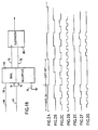
- Figures 1A and 1 B together form a schematic block circuit diagram; and
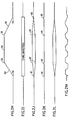
- Figures 2A to 2M illustrate the nature of the signals prevailing at certain points in the circuit.
- Referring to Figures 1A and 1B, a fixed
frequency 20MHz oscillator 10 is connected to acounter 12 which, in conjunction with ashift register 14, serves to produce four 5MHz outputs 16 which are phase shifted by 90° with respect to one another. Any one of theoutputs 16 may be selected byphase selection circuitry 18, e.g. manually operable switches located on a control console, and coupled to a dual multiplier (see Figure 1B) viabuffer amplifier 20, analogue switching circuitry 22 (e.g. FET switches) and buffer/lowpass filter section 24 which blocks frequencies exceeding 5 MHz. - The output of the
counter 12 is connected to adivider chain 26 which provides a gating pulse online 28 which may define a gating period and three pulse trains onlines 30, the pulse trains being different subdivisions of the gating pulse, e.g. so that there are 1, 2 or 4 pulses respectively within the gating interval (see the waveforms of Figures 2A, B, C and D). Figure 2A represents the gating pulses and it will be noted that the other three waveforms are multiples of this. The pulse trains onlines 30 govern whether the calibration signals produced will simulate a single echo or a multiple echo response, i.e. 1, 2 or 4 echoes in the example illustrated. - Selection of a single or multiple echo simulation is effected by means of
circuitry 32 which may comprise a number of manually operable switches for routing the signal on a selected one of thelines 30 tocircuitry 34 for controlling generation of the envelope of the simulated pulses. Figures 2E, 2F and 2G illustrate the waveforms that may be applied to thecircuit 34, according to the selection made. Thecontrol circuitry 34 also receives inputs fromcircuits circuits - In the illustrated embodiment, the
circuit 32 may also be used for controlling the relative timing of the simulated echo pulses in relation to the leading edge of the gating pulses, i.e. so as to simulate echos returned from targets at different positions. In this context, it will be seen that the leading edges of the pulse trains on lines 30 (see Figures 2B and 2D) subdivide the gating pulse (Figure 2A) into one, two or four and consequently the leading edges of the echo pulser provide seven timing increments with respect to the leading edges of the gating pulses. In a modification however, the pulse timing facility may be divorced from the single/multi-echo selection circuit 32. - The
envelope control circuit 34 includes a capacitor charging and discharging of which governs the rise and fall times of the envelope. Thecircuits circuit 36 serves to produce a timing pulse whose duration determines the duration of the plateau of the envelope, as will be explained further below. - The output side of the capacitor is connected to the dual multiplier (Figure 1B) via
buffer section 44, operation of theanalogue switching section 22 being controlled by the envelope control section so that the switches are closed only for the duration of the envelope. The envelope signal produced at the output ofcircuit 34 is coupled to acomparator section 46 which is also coupled to apotentiometer circuit 48. Thecircuit 48 enables the amplitude of the envelope to be set to a selected fixed value. - In operation, when the generation of the envelope is initiated by a pulse from
selection circuit 32, charging of the capacitor commences and follows the usual exponential curve, the time constant being determined by means ofcircuit 38. Thus, the output of thecircuit 34 follows the voltage level of the capacitor and this, in turn, is compared bycircuit 46 with the predetermined amplitude set by the potentiometer. When the capacitor voltage level reaches this preset value, the capacitor is open circuited to prevent further charging and a pulse fromcircuit 36 is then generated to maintain this condition for the required length of time during which time the output of thecircuit 34 will remain substantially constant at the amplitude value preset by means ofcircuit 48. When this time duration is completed, in response to the trailing edge of the pulse applied bycircuit 36, the capacitor is coupled to a selected resistor or resistor combination associated withcircuit 40 so that the capacitor proceeds to discharge with a preset time constant. The falling voltage level is compared bycircuit 46 with a zero reference level and when the latter level is reached, thecomparator section 46 produces an output to reset the envelope control circuit in preparation for the next cycle of envelope generation. - The envelope generated and supplied to the multiplier must not go negative. This is ensured by
buffer 44. As shown in Figure 2H, the envelope will be seen to comprise a risingedge 50, a fallingedge 52 and aconstant amplitude plateau 54. Although the rising and falling edges are of an exponential nature, they may be substantially linear if only a minor part of the exponential curves associated with the capacitor (and resistor combination) are utilised. Thetransition points 56 will in general be of a discontinuous nature and are therefore potential sources of high frequency components during subsequent handling by the multiplier. Figure 2M illustrates the wave form of the 5 MHz signal and it will be understood that this will be confined to a time interval corresponding to the duration of the envelope, i.e. by virtue of a control signal applied to the switching section vialine 60. This is indicated by the waveform as depicted at 21 which illustrates the envelope of the 5 MHz signal without showing the fine detail of the high frequency signal. - Referring now to Figure 1 B, the signals on
lines multiplier 66 which is constituted by the circuit component AD539 manufactured by Analogue Devices. This device has two sets of multiplier inputs, i.e. 68, 70 and 72, 74 andoutputs outputs inputs inputs inputs inputs inputs input 68 and theinput 72 is connected to the ground plane. - As previously mentioned, the envelope (Figure 2H) includes
discontinuities 56 which can give rise to significant and undesirable high frequency feedthrough components during multiplication. This is offset to some extent by the fact that theinputs circuit 80, e.g. a differential amplifier. This is illustrated by the waveform of Figures 2J and 2L. - Figure 2J represents the product signal at
output 76 from which it will be seen thatunwanted feedthrough components 82 are present. Likewise in the case of the product signal at output 78-see Figure 2K. After subtraction however, the resulting output is substantially freed of the feedthrough components-see Figure 2L. It will be understood that the waveform of Figure 2L will be used as an echo simulating calibration pulse and that various parameters thereof can be readily varied, e.g. pulse duration, rise time, fall time and timing relative to the gating pulses. In addition, the phase relationship between the envelope and the carrier may be varied.
Claims (4)
Applications Claiming Priority (4)
| Application Number | Priority Date | Filing Date | Title |
|---|---|---|---|
| GB8428182 | 1984-11-07 | ||
| GB848428182A GB8428182D0 (en) | 1984-11-07 | 1984-11-07 | Signal synthesiser |
| GB8504512 | 1985-02-21 | ||
| GB08504512A GB2166869B (en) | 1984-11-07 | 1985-02-21 | Signal synthesiser |
Publications (2)
| Publication Number | Publication Date |
|---|---|
| EP0181126A1 EP0181126A1 (en) | 1986-05-14 |
| EP0181126B1 true EP0181126B1 (en) | 1988-12-14 |
Family
ID=26288430
Family Applications (1)
| Application Number | Title | Priority Date | Filing Date |
|---|---|---|---|
| EP85307700A Expired EP0181126B1 (en) | 1984-11-07 | 1985-10-24 | Signal synthesiser |
Country Status (4)
| Country | Link |
|---|---|
| US (1) | US4794552A (en) |
| EP (1) | EP0181126B1 (en) |
| DE (1) | DE3566839D1 (en) |
| ES (1) | ES8704680A1 (en) |
Families Citing this family (6)
| Publication number | Priority date | Publication date | Assignee | Title |
|---|---|---|---|---|
| US5268847A (en) * | 1990-12-17 | 1993-12-07 | United Technologies Corporation | Digital synthesis of waveforms |
| US6594821B1 (en) | 2000-03-30 | 2003-07-15 | Transmeta Corporation | Translation consistency checking for modified target instructions by comparing to original copy |
| DE10244650A1 (en) * | 2002-09-25 | 2004-04-08 | Siemens Ag | Calibration system, in particular for a vibration measurement system |
| US9338021B2 (en) | 2005-05-03 | 2016-05-10 | Trend Micro Incorporated | Network traffic redirection in bi-planar networks |
| US8413162B1 (en) | 2005-06-28 | 2013-04-02 | Guillermo J. Rozas | Multi-threading based on rollback |
| CN110221279B (en) * | 2019-06-21 | 2023-03-03 | 瑞纳智能设备股份有限公司 | Automatic detection system and detection method for ultrasonic transducer |
Family Cites Families (10)
| Publication number | Priority date | Publication date | Assignee | Title |
|---|---|---|---|---|
| US3275851A (en) * | 1964-02-18 | 1966-09-27 | Bell Telephone Labor Inc | Trapezoidal test signal generator with leading and trailing edge control |
| US4057778A (en) * | 1976-11-01 | 1977-11-08 | The United States Of America As Represented By The Secretary Of The Navy | Built-in test equipment for sonobuoy |
| US4099240A (en) * | 1977-01-14 | 1978-07-04 | Hewlett-Packard Company | Method and apparatus for programmable and remote numeric control and calibration of electronic instrumentation |
| US4204261A (en) * | 1978-03-01 | 1980-05-20 | The Valeron Corporation | Complex analog signal generator |
| JPS55120242A (en) * | 1979-03-07 | 1980-09-16 | Sharp Corp | Waveform synthesizer |
| DE2945200C2 (en) * | 1979-11-09 | 1983-05-26 | Krautkrämer GmbH, 5000 Köln | Method and circuit device for generating sawtooth pulses and the use of such circuit devices in ultrasonic measuring devices |
| US4316259A (en) * | 1980-03-18 | 1982-02-16 | Grumman Aerospace Corporation | Programmable function generator |
| US4391124A (en) * | 1981-02-26 | 1983-07-05 | Cornell Research Foundation, Inc. | Electroacoustic transducer calibration method and apparatus |
| US4438466A (en) * | 1982-04-02 | 1984-03-20 | Ampex Corporation | D.C. Controlled adjustable ramp signal generator and method |
| US4581585A (en) * | 1983-02-07 | 1986-04-08 | Tektronix, Inc. | Apparatus and method for automatically calibrating a sweep waveform generator |
-
1985
- 1985-10-24 EP EP85307700A patent/EP0181126B1/en not_active Expired
- 1985-10-24 DE DE8585307700T patent/DE3566839D1/en not_active Expired
- 1985-10-31 US US06/793,263 patent/US4794552A/en not_active Expired - Fee Related
- 1985-11-07 ES ES548643A patent/ES8704680A1/en not_active Expired
Also Published As
| Publication number | Publication date |
|---|---|
| ES8704680A1 (en) | 1987-04-01 |
| US4794552A (en) | 1988-12-27 |
| EP0181126A1 (en) | 1986-05-14 |
| DE3566839D1 (en) | 1989-01-19 |
| ES548643A0 (en) | 1987-04-01 |
Similar Documents
| Publication | Publication Date | Title |
|---|---|---|
| US4168502A (en) | Digitally controlled signal simulator | |
| GB2089039A (en) | Thickness measurement with ultrasonic pulses | |
| DE809824C (en) | Device for determining the speed of moving objects, in which a Doppler frequency is generated by mixing emitted and reflected vibrations | |
| US4559826A (en) | Precision source of acoustic radiation | |
| US4794552A (en) | Signal synthesizer | |
| US4982196A (en) | Radar target simulator | |
| US4389899A (en) | Apparatus for measuring the speed of flow of flowable media | |
| GB2166869A (en) | Signal synthesiser | |
| US2935609A (en) | Pre-trigger generator | |
| JPS57192876A (en) | Measuring device for average frequency | |
| US3802253A (en) | Ultrasonic biomedical measuring and recording apparatus | |
| US3559159A (en) | Apparatus for varying the angular direction of a concentrated acoustic beam | |
| JP2900416B2 (en) | Ultrasound diagnostic equipment | |
| GB2089602A (en) | Controllable Reference Oscillator | |
| US3965431A (en) | Circuitry for producing pulses with precise predetermined widths | |
| Carini et al. | A digital electronic instrument for measuring sound velocity | |
| US4130795A (en) | Versatile LDV burst simulator | |
| SU828204A1 (en) | Radio signal simulator | |
| SU968769A1 (en) | Controllable phase shifter | |
| Do | Modern methods of improving the range accuracy of CTFM sonars | |
| GB2017445A (en) | Digitally controlled signal simulator | |
| SU892290A2 (en) | Device for measuring sound absorbtion coefficient | |
| US2774036A (en) | Complex wave analyzer | |
| SU600598A1 (en) | Electronic device for tuning musical instruments | |
| SU773911A1 (en) | Adjustable pulse generator |
Legal Events
| Date | Code | Title | Description |
|---|---|---|---|
| PUAI | Public reference made under article 153(3) epc to a published international application that has entered the european phase |
Free format text: ORIGINAL CODE: 0009012 |
|
| AK | Designated contracting states |
Kind code of ref document: A1 Designated state(s): DE FR IT |
|
| 17P | Request for examination filed |
Effective date: 19860731 |
|
| 17Q | First examination report despatched |
Effective date: 19880209 |
|
| GRAA | (expected) grant |
Free format text: ORIGINAL CODE: 0009210 |
|
| AK | Designated contracting states |
Kind code of ref document: B1 Designated state(s): DE FR IT |
|
| ITF | It: translation for a ep patent filed | ||
| REF | Corresponds to: |
Ref document number: 3566839 Country of ref document: DE Date of ref document: 19890119 |
|
| ET | Fr: translation filed | ||
| PLBE | No opposition filed within time limit |
Free format text: ORIGINAL CODE: 0009261 |
|
| STAA | Information on the status of an ep patent application or granted ep patent |
Free format text: STATUS: NO OPPOSITION FILED WITHIN TIME LIMIT |
|
| 26N | No opposition filed | ||
| PGFP | Annual fee paid to national office [announced via postgrant information from national office to epo] |
Ref country code: FR Payment date: 19911007 Year of fee payment: 7 |
|
| ITTA | It: last paid annual fee | ||
| PGFP | Annual fee paid to national office [announced via postgrant information from national office to epo] |
Ref country code: DE Payment date: 19911129 Year of fee payment: 7 |
|
| PG25 | Lapsed in a contracting state [announced via postgrant information from national office to epo] |
Ref country code: FR Effective date: 19930630 |
|
| PG25 | Lapsed in a contracting state [announced via postgrant information from national office to epo] |
Ref country code: DE Effective date: 19930701 |
|
| REG | Reference to a national code |
Ref country code: FR Ref legal event code: ST |