EP0180255B1 - Semiconductor device comprising a bipolar transistor and an insulated-gate fet - Google Patents
Semiconductor device comprising a bipolar transistor and an insulated-gate fet Download PDFInfo
- Publication number
- EP0180255B1 EP0180255B1 EP85201381A EP85201381A EP0180255B1 EP 0180255 B1 EP0180255 B1 EP 0180255B1 EP 85201381 A EP85201381 A EP 85201381A EP 85201381 A EP85201381 A EP 85201381A EP 0180255 B1 EP0180255 B1 EP 0180255B1
- Authority
- EP
- European Patent Office
- Prior art keywords
- region
- field
- effect transistor
- gate
- base
- Prior art date
- Legal status (The legal status is an assumption and is not a legal conclusion. Google has not performed a legal analysis and makes no representation as to the accuracy of the status listed.)
- Expired
Links
- 239000004065 semiconductor Substances 0.000 title claims description 33
- 230000005669 field effect Effects 0.000 claims description 58
- 230000000295 complement effect Effects 0.000 claims description 6
- 239000004020 conductor Substances 0.000 claims description 4
- 238000000605 extraction Methods 0.000 description 16
- 238000001465 metallisation Methods 0.000 description 13
- 230000010354 integration Effects 0.000 description 5
- 238000002347 injection Methods 0.000 description 4
- 239000007924 injection Substances 0.000 description 4
- 238000009792 diffusion process Methods 0.000 description 3
- 239000000758 substrate Substances 0.000 description 3
- VYPSYNLAJGMNEJ-UHFFFAOYSA-N Silicium dioxide Chemical compound O=[Si]=O VYPSYNLAJGMNEJ-UHFFFAOYSA-N 0.000 description 2
- 229910052796 boron Inorganic materials 0.000 description 2
- 238000000151 deposition Methods 0.000 description 2
- 230000008021 deposition Effects 0.000 description 2
- 238000010586 diagram Methods 0.000 description 2
- 238000005468 ion implantation Methods 0.000 description 2
- 238000004519 manufacturing process Methods 0.000 description 2
- 239000000463 material Substances 0.000 description 2
- 230000004048 modification Effects 0.000 description 2
- 238000012986 modification Methods 0.000 description 2
- ZOXJGFHDIHLPTG-UHFFFAOYSA-N Boron Chemical compound [B] ZOXJGFHDIHLPTG-UHFFFAOYSA-N 0.000 description 1
- OAICVXFJPJFONN-UHFFFAOYSA-N Phosphorus Chemical compound [P] OAICVXFJPJFONN-UHFFFAOYSA-N 0.000 description 1
- XAGFODPZIPBFFR-UHFFFAOYSA-N aluminium Chemical compound [Al] XAGFODPZIPBFFR-UHFFFAOYSA-N 0.000 description 1
- 229910052782 aluminium Inorganic materials 0.000 description 1
- 239000004411 aluminium Substances 0.000 description 1
- 229910052785 arsenic Inorganic materials 0.000 description 1
- RQNWIZPPADIBDY-UHFFFAOYSA-N arsenic atom Chemical class [As] RQNWIZPPADIBDY-UHFFFAOYSA-N 0.000 description 1
- HAYXDMNJJFVXCI-UHFFFAOYSA-N arsenic(5+) Chemical compound [As+5] HAYXDMNJJFVXCI-UHFFFAOYSA-N 0.000 description 1
- 150000001638 boron Chemical class 0.000 description 1
- 239000000969 carrier Substances 0.000 description 1
- 239000002800 charge carrier Substances 0.000 description 1
- 238000011982 device technology Methods 0.000 description 1
- 230000003292 diminished effect Effects 0.000 description 1
- 239000002019 doping agent Substances 0.000 description 1
- 238000005516 engineering process Methods 0.000 description 1
- 230000000873 masking effect Effects 0.000 description 1
- 239000000203 mixture Substances 0.000 description 1
- 229910021421 monocrystalline silicon Inorganic materials 0.000 description 1
- 238000000059 patterning Methods 0.000 description 1
- 229910052698 phosphorus Inorganic materials 0.000 description 1
- 239000011574 phosphorus Substances 0.000 description 1
- 229920002120 photoresistant polymer Polymers 0.000 description 1
- 229910021420 polycrystalline silicon Inorganic materials 0.000 description 1
- 230000002265 prevention Effects 0.000 description 1
- 235000012239 silicon dioxide Nutrition 0.000 description 1
- 239000000377 silicon dioxide Substances 0.000 description 1
- 230000001052 transient effect Effects 0.000 description 1
Images

Classifications
-
- H—ELECTRICITY
- H03—ELECTRONIC CIRCUITRY
- H03K—PULSE TECHNIQUE
- H03K17/00—Electronic switching or gating, i.e. not by contact-making and –breaking
- H03K17/51—Electronic switching or gating, i.e. not by contact-making and –breaking characterised by the components used
- H03K17/56—Electronic switching or gating, i.e. not by contact-making and –breaking characterised by the components used by the use, as active elements, of semiconductor devices
- H03K17/567—Circuits characterised by the use of more than one type of semiconductor device, e.g. BIMOS, composite devices such as IGBT
-
- H—ELECTRICITY
- H10—SEMICONDUCTOR DEVICES; ELECTRIC SOLID-STATE DEVICES NOT OTHERWISE PROVIDED FOR
- H10D—INORGANIC ELECTRIC SEMICONDUCTOR DEVICES
- H10D84/00—Integrated devices formed in or on semiconductor substrates that comprise only semiconducting layers, e.g. on Si wafers or on GaAs-on-Si wafers
- H10D84/40—Integrated devices formed in or on semiconductor substrates that comprise only semiconducting layers, e.g. on Si wafers or on GaAs-on-Si wafers characterised by the integration of at least one component covered by groups H10D12/00 or H10D30/00 with at least one component covered by groups H10D10/00 or H10D18/00, e.g. integration of IGFETs with BJTs
- H10D84/401—Combinations of FETs or IGBTs with BJTs
- H10D84/403—Combinations of FETs or IGBTs with BJTs and with one or more of diodes, resistors or capacitors
- H10D84/406—Combinations of FETs or IGBTs with vertical BJTs and with one or more of diodes, resistors or capacitors
Definitions
- This invention relates to semiconductor devices comprising both a bipolar transistor and an insulated-gate field-effect transistor, particularly but not exclusively for rapid power switching applications.
- a hybrid connection in a common device package of at least three semiconductor bodies is proposed in the Chen and Chin paper to form a so-called “FET-bipolar combination transistor configuration" having three terminals.
- the transistor configuration consists of the bipolar transistor Q 1 , two FETs Q 2 and Q 3 and a zener diode Z.
- the FETs Q2 and Q 3 have insulated gates connected together and individual source and drain regions which are of the same conductivity type as the emitter and collector regions of the bipolar transistor.
- the FET Q 2 may be formed in the same semiconductor body as the bipolar transistor (as illustrated in Figure 3 of the Chen and Chin paper) and provides current to the base region of the bipolar transistor to turn on the transistor configuration.
- the FET Q 3 which is formed in a separate semiconductor body from that of the bipolar transistor 0 1 provides a gateable connection to the emitter region of the bipolar transistor to open-circuit the emitter when turning off the bipolar transistor 0 1 .
- the zener diode also formed in a separate semiconductor body provides a charge-extraction path from the base region of the bipolar transistor when turning off the bipolar transistor 0 1 .
- FET O2 may be formed in the same body as the bipolar transistor, it is not easy to form the zener diode in the same body (at least not in a compact structure). Furthermore, a disadvantage of using a zener diode for the base charge extraction is that significant transient dissipation occurs at the zener voltage during turn off.
- a semiconductor device comprising a bipolar transistor of vertical configuration having an emitter region of one conductivity type in a base region of the opposite conductivity type, the base region being provided in a higher resistivity body portion of the one conductivity type which forms at least part of a collector region of the bipolar transistor, the device also comprising a first insulated-gate field-effect transistor connected to the base region, characterised in that the device additionally comprises a further insulated-gate field-effect transistor which is of complementary conductivity type to the first field-effect transistor and which has a source region of the one conductivity type beside the emitter region, the first field-effect transistor has a drain region of said opposite conductivity type in said body portion beside the base region and has an insulated gate overlying a channel area in a part of said body portion between the base region and the drain region, the further field-effect transistor has an insulated gate over a channel area between the emitter and source regions to provide a gateable connection between the emitter and source regions, which channel area comprises a portion of at
- the charge extraction from the base region is obtained by the first insulated-gate field-effect transistor, and this first FET together with the further FET which provides the gateable emitter connection are merged in a compact structure with the bipolar transistor in the same semiconductor body.
- the base region where it faces the drain region may function as the source of the merged first FET without requiring additional processing of the base region.
- the source region of the further FET may be formed in the same processing steps as the emitter region of the bipolar transistor.
- the device can be less expensive to manufacture than a hybrid connection of separate device bodies. Furthermore an efficient and rapid turn-off can be achieved with this compact structure of the first and further FETs merged with the respective base and emitter regions on which they operate.
- the use of such a merged first FET for the charge extraction results in reduced dissipation during charge extraction in the turn-off phase.
- This charge is extracted from the base region directly to the drain region of the first FET.
- the further FET is turned off because the gate of the further FET is connected to the gate of the first FET. Turning off the further FET directly interrupts the carrier flow in the underlying channel area to the emitter region and so prevents further charge carrier injection from the emitter region into the base region.
- the merged first and further FETs provided for the base charge extraction and emitter gating can be formed without requiring any additional processing steps, but merely by redesigning the mask layout.
- Such a merged FET structure in accordance with the invention may be used for charge-extraction from the base region in devices where the main current path is through the bipolar transistor, but it may also be used in devices where the main current path is through a field-effect transistor which is formed in the same semiconductor body as the bipolar transistor and which may be connected in, for example, parallel with the bipolar transistor.
- the bipolar transistor with the base charge extraction merged FET and emitter-gating FET may even form part of a larger bipolar device structure.
- the high resistivity body portion in which the base region is provided may be present between the base region and an underlying region of the opposite conductivity type with which the bipolar transistor forms an n-p-n-p thyristor structure.
- a semiconductor device in accordance with the invention may also include other circuit elements, for example a FET which provides current to the base region of the bipolar transistor in a circuit configuration similar to that disclosed in the Chen and Chin paper, but using the merged first FETfor base charge extraction and the merged further FET for emitter gating.
- a FET which provides current to the base region of the bipolar transistor in a circuit configuration similar to that disclosed in the Chen and Chin paper, but using the merged first FETfor base charge extraction and the merged further FET for emitter gating.
- the first field-effect transistor may be one of a pair of first and second insulated-gate field-effect transistors which are of complementary conductivity type and which have a common gate connection to form a push-pull input stage connected to the base region of the bipolar transistor.
- This second field-effect transistor may be of vertical configuration having (a) a drain region formed by at least part of the collector region, (b) a source region of the one conductivity type provided in the base region and connected to the base region by a conductive connection, and (c) an insulated gate overlying a channel area of the base region between said body portion and the source region of the second field-effect transistor.
- Figures 1, 2 and 4 are diagrammatic and not drawn to scale. The relative dimensions and proportions of parts of these Figures (particularly in the direction of thickness in the cross-sections of Figures 2 and 4) have been shown exaggerated or diminished for the sake of clarity and convenience in the drawings.
- the same reference signs as used in one embodiment are generally used when referring to corresponding or similar parts in other embodiments.
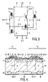
- the semiconductor device of Figures 1 and 2 comprises a bipolar transistor T of vertical configuration having an emitter region 1 of, for example, n type conductivity in a base region 2 of the opposite conductivity type (p type in this example).
- the base region 2 is provided in a higher resistivity body portion 30 of the first conductivity (n type) which forms a part of a collector region 3 of the bipolartransistor T.
- the collector region also comprises a highly- doped n type substrate 31 on which the body portion 30 is provided as an epitaxial layer.
- the device additionally comprises first, second, third and fourth insulated-gate field-effect transistors T1, T2, T3, T4 which are integrated and merged with the bipolar transistor T in the same semiconductor body 10 to form a device arrangement in accordance with a preferred embodiment of the invention and with an equivalent circuit configuration as illustrated in Figure 3.
- the device of Figures 1 and 2 is characterised in that the first field-effect transistor T1 has a drain region 5 of said opposite conductivity type (p type) in the body portion 30 beside the base region 2 and has an insulated gate 6 overlying a channel area 7 in a part of the body portion 30 between the drain region 5 and the base region 2, the adjacent part of which acts as the source of T1.
- the transistor T1 formed in this manner provides a charge extraction path from the base region 2 when the bipolar transistor T is turned off.
- the device further comprises in accordance with the invention a further insulated-gate field-effect transistor T3 which is of complementary conductivity type to the p channel first field-effect transistor T1 and which has a source region 11 of the first conductivity type (n type) beside the emitter region 1, the adjacent part of which acts asthedrain ofT3.
- This further transistor T3 has an insulated gate 12 over a channel area 13 between the emitter and source regions 1 and 11. In the Example of Figures 1 and 2, this channel area 13 comprises a portion of both the base region 2 and the drain region 5.
- the gate 12 of T3 is connected to the gate 6 ofT1 so permitting T1 to be turned on to extract charge from the base region 2 when T3 is turned off by a signal applied to its gate 12.
- the gates 6 and 12 in the example of Figures 1 and 2 are formed by a common grid of conductive material.
- the drain region 5 ofT1 is connected to the source region 11 of T3.
- the device comprises a compact two-dimensional array of alternating separate p type regions 2 and 5 side- by-side in the n type body portion 30.
- the source regions 11 of T3 are provided in the regions 5 which form the drain of T1.
- the insulated gate 12 of T3 overlies both an intermediate part 14 of the body portion 30 between the regions 2 and 5 and the adjacent channel area 13 in the regions 2 and 5 to control current flow from the source regions 11 both laterally to the emitter regions 1 and vertically to the regions 30 and 31 which provide the collector 3 of T.
- a vertical insulated-gate field-effect transistor having a gate 12, channel area 13, region 11 as its source, and regions 30 and 31 as its drain.
- the source regions 11 are connected to the region 5 by a conductive connection formed by metallization pattern 20.
- This provides a particularly efficient means of forming the connection between the source of T3 and the drain of T1 at each cell of the array and also serves to suppress bipolar transistor action between the regions 11 and the body portion 30.
- the device of Figures 1 and 2 can be designed so that the main current path through the device between terminals C/D and E/S in Figure 3 is either by bipolar transistor action through T or FET action through T4 or is approximately equally divided between T and T4.
- the first field-effect transistor T1 is one of a pair of first and second insulated-gate field-effect transistors which are of complementary conductivity type and which have a common gate connection to form a push-pull input stage the output of which is connected to the base region 2 of the bipolar transistor T.
- This second field-effect transistor T2 is of vertical configuration having (a) a drain region formed by a part of the n type regions 30 and 31, (b) a source region 15 of the same conductivity type (n type) provided in the base region 2 and connected to the base region 2 by a metallization pattern 22, and (c) an insulated gate 6 which overlies a channel area 16 of base region 2 between the body portion 30 and the source region 15 of T2.
- T2 is integrated and merged with the other transistors of the device in a very compact arrangement.
- the part of the base region 2 in which its source region 15 is provided also forms the source region of T1, and both T1 and T2 have a common insulated gate. This is much more compact than the integration of Q2 illustrated in Figure 3 of the previously mentioned Chen and Chin paper.
- the base and drain regions 2 and 5 in this particular example are four-sided in plan view.
- the base charge extraction transistor T1 is formed along two adjacent sides of each of the drain regions 5, while the emitter gating transistor T3 is formed with its source region 11 along the other two adjacent sides of each of the region 5.
- This provides a very compact array geometry, particularly as the second transistor T2 of the input stage pair is merged into the array by the provision of its source regions 15 at the adjacent sides of the base regions 2 facing the charge extraction transistor T 1 .
- n type source region which may be similar to region 15 can be provided at a part of the adjacent sides of the drain regions 5 where T1 is formed.
- the gates 12 and 6 of all the insulated-gate field-effect transistor T1 to T4 are formed in this particular example by a common rectangular grid of conductive material which extends on a part of the insulating layer 25 over the area between the base and drain regions 2 and 5.
- the device of Figures 1 and 2 can be manufactured using known power semiconductor device technology, for example as used to manufacture power FETs of the so-called D-MOST type.
- the mask geometry used with the technology is however adapted to produce the region layout of Figures 1 and 2.
- the body 10 may be of monocrystalline silicon, and the portion 30 may be grown as a high resistivity n type epitaxial layer on a highly doped n type substrate 31.
- An insulating layer 25 of silicon dioxide may be thermally grown on the surface of the epitaxial layer. Where the insulated gates are to be formed, the composition and thickness of the layer 25 is chosen to provide the desired gate dielectric for the transistor T1 to T4.
- the gate grid is formed on the layer 25 by deposition and patterning a suitable material such as polycrystalline silicon which may be doped either during or after deposition so as to render it conductive.
- the p type regions 2 and 5 may be formed in the epitaxial layer by, for example, boron ion implantation and/or diffusion. In known manner, the gate grid 12,6 is used to mask this boron doping so defining the array of separate regions 2 and 5.
- the n type regions 1, 11 and 15 may be formed in the p type regions 2 and 5 by, for example, phosphorus or arsenic ion implantation and/or diffusion. This arsenic doping is masked by the gate grid 12,6 and by a further masking pattern of, for example, photoresist which covers selected areas of the p type regions 2 and 5 within the apertures in the gate grid 2, 5.
- the insulating layer 25 is then provided with contact windows as illustrated in broken lines (- - -) in Figure 1. As shown in Figure 1 there is a small window for contacting the base 2 of T and source 15 of T2 and a large window for contacting the drain 5 of T1 and the source 11 of T3. Conductive material, for example aluminium is then deposited and patterned to form the upper level metallization patterns, for example parts 20 and 22.
- Metallization 20 is in the form of a sheet which covers most of the upper surface of the device array and which contracts the top surface of the semiconductor body 10 at the large contact windows of the layer 25 so forming the emitter/source terminal connection (E/S) of the device as illustrated in Figure 3. This metallization sheet 20 has apertures therein over the base region 2.
- the metallization pattern 22 is located within these apertures and contacts the top surface of the semiconductor body 10 at the small contact windows of the layer 25. There is no terminal connection to this metallization 22 which floats at its own potential as determined by the regions 2 and 15. There is a further part of the upper level metallization which provides a terminal connection B/G to the gate grid 12, 6 and which is not shown in Figure 1 and 2.
- the bottom surface of the substrate 31 is coated with metallization 21 which provides terminal connection C/D of Figure 3. In this manner a total device having just three terminal connections is obtained, the main current path being between E/S and C/D and being controlled by a signal applied to B/G.
- the device of Figures 1 to 3 can be operated with its terminal C/D at a high positive potential with respect to its terminal E/S.
- 6 By applying a positive potential to the control terminal B/G the gate grid 12, 6 is biased positive.
- T1 is off but T2 and T3 are turned on.
- T2 on current flows via the metallization short 22 from its source 15 to the base 2 of the bipolar transistor T.
- the turning on of T3 completes the connection between terminal E/S and the emitter 1 of the bipolar transistor so completing the cascode connection of T and T3.
- the current path from T3 to terminal C/D is split between the vertical bipolar transistor T and the vertical insulated-gate field-effect transistor T4 connected in parallel with T.
- the device can be designed to have a particular desired degree of minority-carrier injection so that the device may be designed as a gated bipolar transistor or as a minority-carrier injected insulated-gate field-effect transistor depending on how much of the current is carried by T and T4 respectively.
- the drive to the bipolar transistor T is removed by turning offT2; the gated connection to the emitter 1 of the bipolar transistor T and to the source 11 of the parallel FET T4 is also broken by turning off T3.
- the p channel FET T1 turns on thus connecting together the base and drain regions 2 and 5 and allowing the minority carriers associated with the bipolar transistor action to be extracted from the base region 2 via the metallization 20.
- the width of the gap between the two p type regions 2 and 5 governs the degree of body-effect modulation of the threshold voltage ofT1 during turn off.
- the device of Figure 1 and 2 has the advantages of a high input impedance resulting from the integration of the FET T2 and a fast turn off resulting from the integration of the base charge extraction FETT1 and the emitter gating FETT3.
- the device of Figures 1 and 2 has the advantage of minority carrier injection resulting from the integration of the bipolar transistor T which reduces the ON resistance.
- the device arrangement is still very compact and is integrated in a single semiconductor body 10 with only three terminal connections.
- Figure 4 illustrates a modification in which the n type high resistivity body portion 30 is present between the p type base region 2 and an underlying p type anode region 40 which forms with the bipolar transistor T an n-p-n-p thyristor structure into which the insulated-gate field-effect transistors T1, T2, T3 and T4 are merged.
- the provision of the anode region 40 allows the bipolar section of the device to latch under forward conduction so that once turned on by a signal at terminal B/G, it can only be turned off by reducing the potential on terminal C/D.
- the anode region 40 may comprise an array of apertures at which the bottom metallization 21 is connected to the body portion 30 via an array of n type contact regions 41 to short-circuit a part of the anode p-n junction.
- the portion 30 may be formed by the bulk of the body 10 (instead of by an epitaxial layer) and the regions 40 and 41 may be formed by dopant diffusion at its back surface.
- devices in accordance with the present invention may be designed with a less compact geometry in which, for example, separate p type regions are used instead of a common region 5 for the drain of T1 and for the channel area of T3.
- the input transistor T2 may also be omitted.
- the FETs illustrated in Figures 2 and 4 have their insulated gates at the top main surface of the body 10, at least some of these FETs may have insulated gates formed on the side-walls of grooves in the top main surface of the body 10.
Landscapes
- Metal-Oxide And Bipolar Metal-Oxide Semiconductor Integrated Circuits (AREA)
- Bipolar Transistors (AREA)
- Logic Circuits (AREA)
Description
- This invention relates to semiconductor devices comprising both a bipolar transistor and an insulated-gate field-effect transistor, particularly but not exclusively for rapid power switching applications.
- The paper entitled "Design Considerations for FET-Gated Power Transistors" by D. Y. Chen and S. A. Chin, pages 144 to 149 of the 1983 IEEE Proceedings of the Power Electronic Specialist Conference, IEEE publication 0275-9306/83/0000-0144, describes a semiconductor device comprising a bipolar transistor of vertical configuration having an emitter region of one conductivity type in a base region of the opposite conductivity type. The base region is provided in a higher resistivity body portion of the one conductivity type which forms at least part of a collector region of the bipolar transistor. The device additionally comprises an insulated-gate field-effect transistor (designated as FET) connected to the base region.
- A hybrid connection in a common device package of at least three semiconductor bodies (called "chips") is proposed in the Chen and Chin paper to form a so-called "FET-bipolar combination transistor configuration" having three terminals. The transistor configuration consists of the bipolar transistor Q1, two FETs Q2 and Q3 and a zener diode Z. The FETs Q2 and Q3 have insulated gates connected together and individual source and drain regions which are of the same conductivity type as the emitter and collector regions of the bipolar transistor.
- The FET Q2 may be formed in the same semiconductor body as the bipolar transistor (as illustrated in Figure 3 of the Chen and Chin paper) and provides current to the base region of the bipolar transistor to turn on the transistor configuration. The FET Q3 which is formed in a separate semiconductor body from that of the bipolar transistor 01 provides a gateable connection to the emitter region of the bipolar transistor to open-circuit the emitter when turning off the bipolar transistor 01. The zener diode also formed in a separate semiconductor body provides a charge-extraction path from the base region of the bipolar transistor when turning off the bipolar transistor 01.
- This hybrid connection of at least three semiconductor device bodies results in an expensive device arrangement. Although FET O2 may be formed in the same body as the bipolar transistor, it is not easy to form the zener diode in the same body (at least not in a compact structure). Furthermore, a disadvantage of using a zener diode for the base charge extraction is that significant transient dissipation occurs at the zener voltage during turn off.
- According to the present invention there is provided a semiconductor device comprising a bipolar transistor of vertical configuration having an emitter region of one conductivity type in a base region of the opposite conductivity type, the base region being provided in a higher resistivity body portion of the one conductivity type which forms at least part of a collector region of the bipolar transistor, the device also comprising a first insulated-gate field-effect transistor connected to the base region, characterised in that the device additionally comprises a further insulated-gate field-effect transistor which is of complementary conductivity type to the first field-effect transistor and which has a source region of the one conductivity type beside the emitter region, the first field-effect transistor has a drain region of said opposite conductivity type in said body portion beside the base region and has an insulated gate overlying a channel area in a part of said body portion between the base region and the drain region, the further field-effect transistor has an insulated gate over a channel area between the emitter and source regions to provide a gateable connection between the emitter and source regions, which channel area comprises a portion of at least the base region, and the gate of the further field-effect transistor is connected to the gate of the first field-effect transistor so permitting the first field-effect transistor to be turned on to extract charge from the base region to the drain region of the first field-effect transistor when the further field-effect transistor is turned off by a signal applied to its gate.
- In such a semiconductor device in accordance with the invention the charge extraction from the base region is obtained by the first insulated-gate field-effect transistor, and this first FET together with the further FET which provides the gateable emitter connection are merged in a compact structure with the bipolar transistor in the same semiconductor body. The base region where it faces the drain region may function as the source of the merged first FET without requiring additional processing of the base region. The source region of the further FET may be formed in the same processing steps as the emitter region of the bipolar transistor. The device can be less expensive to manufacture than a hybrid connection of separate device bodies. Furthermore an efficient and rapid turn-off can be achieved with this compact structure of the first and further FETs merged with the respective base and emitter regions on which they operate.
- Compared with a zener diode, the use of such a merged first FET for the charge extraction results in reduced dissipation during charge extraction in the turn-off phase. This charge is extracted from the base region directly to the drain region of the first FET. When the first FET is turned on to extract this base charge, the further FET is turned off because the gate of the further FET is connected to the gate of the first FET. Turning off the further FET directly interrupts the carrier flow in the underlying channel area to the emitter region and so prevents further charge carrier injection from the emitter region into the base region. The integration and merging of the base-charge extraction FET and the emitter-injection prevention FET with the respective base and emitter regions with which they perform these respective functions permits these FETs to cooperate efficiently in this manner to provide rapid turn-off of the device.
- Particularly where the semiconductor device already includes an insulated-gate FET in addition to the bipolar transistor, the merged first and further FETs provided for the base charge extraction and emitter gating can be formed without requiring any additional processing steps, but merely by redesigning the mask layout.
- Such a merged FET structure in accordance with the invention may be used for charge-extraction from the base region in devices where the main current path is through the bipolar transistor, but it may also be used in devices where the main current path is through a field-effect transistor which is formed in the same semiconductor body as the bipolar transistor and which may be connected in, for example, parallel with the bipolar transistor. The bipolar transistor with the base charge extraction merged FET and emitter-gating FET may even form part of a larger bipolar device structure. Thus, for example, the high resistivity body portion in which the base region is provided may be present between the base region and an underlying region of the opposite conductivity type with which the bipolar transistor forms an n-p-n-p thyristor structure.
- A semiconductor device in accordance with the invention may also include other circuit elements, for example a FET which provides current to the base region of the bipolar transistor in a circuit configuration similar to that disclosed in the Chen and Chin paper, but using the merged first FETfor base charge extraction and the merged further FET for emitter gating.
- Thus, the first field-effect transistor may be one of a pair of first and second insulated-gate field-effect transistors which are of complementary conductivity type and which have a common gate connection to form a push-pull input stage connected to the base region of the bipolar transistor. This second field-effect transistor may be of vertical configuration having (a) a drain region formed by at least part of the collector region, (b) a source region of the one conductivity type provided in the base region and connected to the base region by a conductive connection, and (c) an insulated gate overlying a channel area of the base region between said body portion and the source region of the second field-effect transistor.
- These and other features in accordance with the invention will be illustrated more specifically, by way of example, in embodiments of the invention now to be described with reference to the accompanying diagrammatic drawings, in which:
- Figure 1 is a plan view of part of a semiconductor device body of a device in accordance with the invention;
- Figure 2 is a cross-section on the line 11-11 of Figure 1;
- Figure 3 is an equivalent circuit diagram of the integrated and merged circuit elements of such a semiconductor device in accordance with the invention, and
- Figure 4 is a cross-section of part of another semiconductor device in accordance with the invention.
- It should be noted that Figures 1, 2 and 4 are diagrammatic and not drawn to scale. The relative dimensions and proportions of parts of these Figures (particularly in the direction of thickness in the cross-sections of Figures 2 and 4) have been shown exaggerated or diminished for the sake of clarity and convenience in the drawings. The same reference signs as used in one embodiment are generally used when referring to corresponding or similar parts in other embodiments.
- The semiconductor device of Figures 1 and 2 comprises a bipolar transistor T of vertical configuration having an
emitter region 1 of, for example, n type conductivity in abase region 2 of the opposite conductivity type (p type in this example). Thebase region 2 is provided in a higherresistivity body portion 30 of the first conductivity (n type) which forms a part of acollector region 3 of the bipolartransistor T. ln the example of Figures 1 and 2 the collector region also comprises a highly- dopedn type substrate 31 on which thebody portion 30 is provided as an epitaxial layer. The device additionally comprises first, second, third and fourth insulated-gate field-effect transistors T1, T2, T3, T4 which are integrated and merged with the bipolar transistor T in thesame semiconductor body 10 to form a device arrangement in accordance with a preferred embodiment of the invention and with an equivalent circuit configuration as illustrated in Figure 3. - In accordance with the present invention the device of Figures 1 and 2 is characterised in that the first field-effect transistor T1 has a
drain region 5 of said opposite conductivity type (p type) in thebody portion 30 beside thebase region 2 and has aninsulated gate 6 overlying achannel area 7 in a part of thebody portion 30 between thedrain region 5 and thebase region 2, the adjacent part of which acts as the source of T1. The transistor T1 formed in this manner provides a charge extraction path from thebase region 2 when the bipolar transistor T is turned off. - In addition to T1 the device further comprises in accordance with the invention a further insulated-gate field-effect transistor T3 which is of complementary conductivity type to the p channel first field-effect transistor T1 and which has a
source region 11 of the first conductivity type (n type) beside theemitter region 1, the adjacent part of which acts asthedrain ofT3. This further transistor T3 has an insulatedgate 12 over achannel area 13 between the emitter andsource regions channel area 13 comprises a portion of both thebase region 2 and thedrain region 5. Thegate 12 of T3 is connected to thegate 6 ofT1 so permitting T1 to be turned on to extract charge from thebase region 2 when T3 is turned off by a signal applied to itsgate 12. As described below thegates drain region 5 ofT1 is connected to thesource region 11 of T3. - As can be seen from Figures 1 and 2, the device comprises a compact two-dimensional array of alternating separate
p type regions type body portion 30. Thesource regions 11 of T3 are provided in theregions 5 which form the drain of T1. Theinsulated gate 12 of T3 overlies both anintermediate part 14 of thebody portion 30 between theregions adjacent channel area 13 in theregions source regions 11 both laterally to theemitter regions 1 and vertically to theregions collector 3 of T. Thus there is formed, in parallel with the bipolar transistor T, a vertical insulated-gate field-effect transistor having agate 12,channel area 13,region 11 as its source, andregions source regions 11 are connected to theregion 5 by a conductive connection formed bymetallization pattern 20. This provides a particularly efficient means of forming the connection between the source of T3 and the drain of T1 at each cell of the array and also serves to suppress bipolar transistor action between theregions 11 and thebody portion 30. By adjusting the relative areas of theregions regions - As can be seen from the circuit diagram of Figures 1 and 2, the first field-effect transistor T1 is one of a pair of first and second insulated-gate field-effect transistors which are of complementary conductivity type and which have a common gate connection to form a push-pull input stage the output of which is connected to the
base region 2 of the bipolar transistor T. This second field-effect transistor T2 is of vertical configuration having (a) a drain region formed by a part of then type regions source region 15 of the same conductivity type (n type) provided in thebase region 2 and connected to thebase region 2 by ametallization pattern 22, and (c) aninsulated gate 6 which overlies achannel area 16 ofbase region 2 between thebody portion 30 and thesource region 15 of T2. As illustrated in Figures 1 and 2, T2 is integrated and merged with the other transistors of the device in a very compact arrangement. The part of thebase region 2 in which itssource region 15 is provided also forms the source region of T1, and both T1 and T2 have a common insulated gate. This is much more compact than the integration of Q2 illustrated in Figure 3 of the previously mentioned Chen and Chin paper. - In order to facilitate understanding of the layout of the device, different outlines have been used in the plan view of Figure 1 and the upper layers have been shown cut-away from the upper rows of the array of Figure 1. In the top row of Figure 1 the alternating
p type regions conductive gate material n type regions regions grid layer 25 at the top surface of thesemiconductor body 10 are shown in broken lines (- - -) in all rows of the array. Thegate grid top metallization patterns - As can be seen from Figure 1 the base and
drain regions drain regions 5, while the emitter gating transistor T3 is formed with itssource region 11 along the other two adjacent sides of each of theregion 5. This provides a very compact array geometry, particularly as the second transistor T2 of the input stage pair is merged into the array by the provision of itssource regions 15 at the adjacent sides of thebase regions 2 facing the charge extraction transistor T1. If it is desired to increase further the efficiency of the vertical field-effect transistor T4 (in parallel with the bipolar transistor T) an additional n type source region which may be similar toregion 15 can be provided at a part of the adjacent sides of thedrain regions 5 where T1 is formed. Thegates layer 25 over the area between the base anddrain regions - The device of Figures 1 and 2 can be manufactured using known power semiconductor device technology, for example as used to manufacture power FETs of the so-called D-MOST type. The mask geometry used with the technology is however adapted to produce the region layout of Figures 1 and 2. Thus, the
body 10 may be of monocrystalline silicon, and theportion 30 may be grown as a high resistivity n type epitaxial layer on a highly dopedn type substrate 31. An insulatinglayer 25 of silicon dioxide may be thermally grown on the surface of the epitaxial layer. Where the insulated gates are to be formed, the composition and thickness of thelayer 25 is chosen to provide the desired gate dielectric for the transistor T1 to T4. The gate grid is formed on thelayer 25 by deposition and patterning a suitable material such as polycrystalline silicon which may be doped either during or after deposition so as to render it conductive. Thep type regions gate grid separate regions n type regions p type regions gate grid p type regions gate grid - The insulating
layer 25 is then provided with contact windows as illustrated in broken lines (- - -) in Figure 1. As shown in Figure 1 there is a small window for contacting thebase 2 of T andsource 15 of T2 and a large window for contacting thedrain 5 of T1 and thesource 11 of T3. Conductive material, for example aluminium is then deposited and patterned to form the upper level metallization patterns, forexample parts Metallization 20 is in the form of a sheet which covers most of the upper surface of the device array and which contracts the top surface of thesemiconductor body 10 at the large contact windows of thelayer 25 so forming the emitter/source terminal connection (E/S) of the device as illustrated in Figure 3. Thismetallization sheet 20 has apertures therein over thebase region 2. Themetallization pattern 22 is located within these apertures and contacts the top surface of thesemiconductor body 10 at the small contact windows of thelayer 25. There is no terminal connection to thismetallization 22 which floats at its own potential as determined by theregions gate grid substrate 31 is coated withmetallization 21 which provides terminal connection C/D of Figure 3. In this manner a total device having just three terminal connections is obtained, the main current path being between E/S and C/D and being controlled by a signal applied to B/G. - The device of Figures 1 to 3 can be operated with its terminal C/D at a high positive potential with respect to its terminal E/S. By applying a positive potential to the control terminal B/G the
gate grid source 15 to thebase 2 of the bipolar transistor T. Simultaneously, the turning on of T3 completes the connection between terminal E/S and theemitter 1 of the bipolar transistor so completing the cascode connection of T and T3. The current path from T3 to terminal C/D is split between the vertical bipolar transistor T and the vertical insulated-gate field-effect transistor T4 connected in parallel with T. As already mentioned by adjusting the relative areas of the regions ofT and T4 and the p-n junction short-circuits the device can be designed to have a particular desired degree of minority-carrier injection so that the device may be designed as a gated bipolar transistor or as a minority-carrier injected insulated-gate field-effect transistor depending on how much of the current is carried by T and T4 respectively. - By applying a negative (or low, depending on the FET threshold voltages) potential to the terminal B/G, the drive to the bipolar transistor T is removed by turning offT2; the gated connection to the
emitter 1 of the bipolar transistor T and to thesource 11 of the parallel FET T4 is also broken by turning off T3. Simultaneously the p channel FET T1 turns on thus connecting together the base anddrain regions base region 2 via themetallization 20. The width of the gap between the twop type regions emitter regions insulated gates - As compared with a simple bipolar transistor, the device of Figure 1 and 2 has the advantages of a high input impedance resulting from the integration of the FET T2 and a fast turn off resulting from the integration of the base charge extraction FETT1 and the emitter gating FETT3. As compared with a simple insulated-gate FET, the device of Figures 1 and 2 has the advantage of minority carrier injection resulting from the integration of the bipolar transistor T which reduces the ON resistance. However, the device arrangement is still very compact and is integrated in a
single semiconductor body 10 with only three terminal connections. - Figure 4 illustrates a modification in which the n type high
resistivity body portion 30 is present between the ptype base region 2 and an underlying ptype anode region 40 which forms with the bipolar transistor T an n-p-n-p thyristor structure into which the insulated-gate field-effect transistors T1, T2, T3 and T4 are merged. The provision of theanode region 40 allows the bipolar section of the device to latch under forward conduction so that once turned on by a signal at terminal B/G, it can only be turned off by reducing the potential on terminal C/D. The provision of the emitter gating transistor T3 and the base charge extraction transistor T1 both merged into this thyristor structure in accordance with the invention has considerable advantages in forcing the turn-off of the thyristor. Also to facilitate charge extraction from thebody portion 30 adjacent theanode region 40 during turn off, theanode region 40 may comprise an array of apertures at which thebottom metallization 21 is connected to thebody portion 30 via an array of ntype contact regions 41 to short-circuit a part of the anode p-n junction. In this case, theportion 30 may be formed by the bulk of the body 10 (instead of by an epitaxial layer) and theregions - It will be evident that many modifications are possible within the scope of the present invention. Thus, for example, although
square regions individual regions p type regions common region 5 for the drain of T1 and for the channel area of T3. The input transistor T2 may also be omitted. Although the FETs illustrated in Figures 2 and 4 have their insulated gates at the top main surface of thebody 10, at least some of these FETs may have insulated gates formed on the side-walls of grooves in the top main surface of thebody 10.
Claims (9)
Applications Claiming Priority (2)
| Application Number | Priority Date | Filing Date | Title |
|---|---|---|---|
| GB8423690 | 1984-09-19 | ||
| GB08423690A GB2164790A (en) | 1984-09-19 | 1984-09-19 | Merged bipolar and field effect transistors |
Publications (3)
| Publication Number | Publication Date |
|---|---|
| EP0180255A2 EP0180255A2 (en) | 1986-05-07 |
| EP0180255A3 EP0180255A3 (en) | 1986-11-20 |
| EP0180255B1 true EP0180255B1 (en) | 1990-02-28 |
Family
ID=10566949
Family Applications (1)
| Application Number | Title | Priority Date | Filing Date |
|---|---|---|---|
| EP85201381A Expired EP0180255B1 (en) | 1984-09-19 | 1985-09-03 | Semiconductor device comprising a bipolar transistor and an insulated-gate fet |
Country Status (5)
| Country | Link |
|---|---|
| US (1) | US4729007A (en) |
| EP (1) | EP0180255B1 (en) |
| JP (1) | JPH0656881B2 (en) |
| DE (1) | DE3576243D1 (en) |
| GB (1) | GB2164790A (en) |
Families Citing this family (16)
| Publication number | Priority date | Publication date | Assignee | Title |
|---|---|---|---|---|
| GB2190539A (en) * | 1986-05-16 | 1987-11-18 | Philips Electronic Associated | Semiconductor devices |
| JPH0654796B2 (en) * | 1986-07-14 | 1994-07-20 | 株式会社日立製作所 | Composite semiconductor device |
| US4847671A (en) * | 1987-05-19 | 1989-07-11 | General Electric Company | Monolithically integrated insulated gate semiconductor device |
| KR900001062B1 (en) * | 1987-09-15 | 1990-02-26 | 강진구 | Manufacturing Method of Semiconductor By Sea Morse Device |
| US4830973A (en) * | 1987-10-06 | 1989-05-16 | Motorola, Inc. | Merged complementary bipolar and MOS means and method |
| US5117274A (en) * | 1987-10-06 | 1992-05-26 | Motorola, Inc. | Merged complementary bipolar and MOS means and method |
| IT1217323B (en) * | 1987-12-22 | 1990-03-22 | Sgs Microelettronica Spa | INTEGRATED STRUCTURE OF HIGH VOLTAGE BIPOLAR POWER TRANSISTOR AND LOW VOLTAGE POWER MOS TRANSISTOR IN THE "EMITTER SWITCHING" CONFIGURATION AND RELATED MANUFACTURING PROCESS |
| US4998156A (en) * | 1988-03-25 | 1991-03-05 | General Electric Company | Structure for a complementary-symmetry COMFET pair |
| US5247200A (en) * | 1989-02-16 | 1993-09-21 | Kabushiki Kaisha Toshiba | MOSFET input type BiMOS IC device |
| DE3941932A1 (en) * | 1989-12-19 | 1991-06-20 | Eupec Gmbh & Co Kg | METHOD FOR PRODUCING ANODE-SIDE SHORT CIRCUITS IN THYRISTORS |
| JPH0421211A (en) * | 1990-05-16 | 1992-01-24 | Toshiba Corp | Method and device for driving semiconductor element |
| JPH0795597B2 (en) * | 1990-08-18 | 1995-10-11 | 三菱電機株式会社 | Thyristor and manufacturing method thereof |
| JPH04280475A (en) * | 1991-03-08 | 1992-10-06 | Fuji Electric Co Ltd | Semiconductor switching device |
| US6004840A (en) * | 1994-04-15 | 1999-12-21 | Kabushiki Kaisha Toshiba | Method of fabricating a semiconductor device comprising a MOS portion and a bipolar portion |
| EP0681319B1 (en) * | 1994-04-15 | 2002-10-30 | Kabushiki Kaisha Toshiba | Semiconductor device and method of manufacturing the same |
| US5913130A (en) * | 1996-06-12 | 1999-06-15 | Harris Corporation | Method for fabricating a power device |
Family Cites Families (6)
| Publication number | Priority date | Publication date | Assignee | Title |
|---|---|---|---|---|
| US3663869A (en) * | 1971-01-26 | 1972-05-16 | Westinghouse Electric Corp | Bipolar-unipolar transistor structure |
| FR2505102B1 (en) * | 1981-04-29 | 1986-01-24 | Radiotechnique Compelec | DARLINGTON AMPLIFIER FORMED BY A FIELD EFFECT TRANSISTOR AND A BIPOLAR TRANSISTOR, AND ITS IMPLEMENTATION IN AN INTEGRATED SEMICONDUCTOR STRUCTURE |
| US4441117A (en) * | 1981-07-27 | 1984-04-03 | Intersil, Inc. | Monolithically merged field effect transistor and bipolar junction transistor |
| US5014102A (en) * | 1982-04-01 | 1991-05-07 | General Electric Company | MOSFET-gated bipolar transistors and thyristors with both turn-on and turn-off capability having single-polarity gate input signal |
| EP0118336B1 (en) * | 1983-02-03 | 1988-04-20 | Fairchild Semiconductor Corporation | High voltage mos/bipolar power transistor apparatus |
| US4611235A (en) * | 1984-06-04 | 1986-09-09 | General Motors Corporation | Thyristor with turn-off FET |
-
1984
- 1984-09-19 GB GB08423690A patent/GB2164790A/en not_active Withdrawn
-
1985
- 1985-09-03 EP EP85201381A patent/EP0180255B1/en not_active Expired
- 1985-09-03 DE DE8585201381T patent/DE3576243D1/en not_active Expired - Lifetime
- 1985-09-17 JP JP60205175A patent/JPH0656881B2/en not_active Expired - Lifetime
- 1985-09-17 US US06/777,066 patent/US4729007A/en not_active Expired - Fee Related
Also Published As
| Publication number | Publication date |
|---|---|
| US4729007A (en) | 1988-03-01 |
| EP0180255A2 (en) | 1986-05-07 |
| JPH0656881B2 (en) | 1994-07-27 |
| DE3576243D1 (en) | 1990-04-05 |
| JPS6177355A (en) | 1986-04-19 |
| GB8423690D0 (en) | 1984-10-24 |
| EP0180255A3 (en) | 1986-11-20 |
| GB2164790A (en) | 1986-03-26 |
Similar Documents
| Publication | Publication Date | Title |
|---|---|---|
| US4729007A (en) | Merged bipolar/field-effect transistors | |
| US5014102A (en) | MOSFET-gated bipolar transistors and thyristors with both turn-on and turn-off capability having single-polarity gate input signal | |
| US6051850A (en) | Insulated gate bipolar junction transistors having built-in freewheeling diodes therein | |
| US6118150A (en) | Insulated gate semiconductor device and method of manufacturing the same | |
| US5897343A (en) | Method of making a power switching trench MOSFET having aligned source regions | |
| US4779123A (en) | Insulated gate transistor array | |
| US5464992A (en) | Insulated gate bipolar transistor provided with a minority carrier extracting layer | |
| US20020056884A1 (en) | Vertical power devices having deep and shallow trenches and methods of forming same | |
| EP0084558B1 (en) | Monolithically merged field effect transistor and bipolar junction transistor | |
| EP0697739B1 (en) | Insulated gate bipolar transistor | |
| EP0159663A2 (en) | High-density V-groove MOS-controlled thyristors, insulated-gate transistors, and MOSFETs, and methods for fabrication | |
| KR100304716B1 (en) | Diode by controlled metal oxide semiconductor & method of fabrication the same | |
| EP0646964B1 (en) | Integrated structure active clamp for the protection of power devices against overvoltages, and manufacturing process thereof | |
| US4314267A (en) | Dense high performance JFET compatible with NPN transistor formation and merged BIFET | |
| GB2241111A (en) | Transistors integrated with diodes | |
| US5357120A (en) | Compound semiconductor device and electric power converting apparatus using such device | |
| US6765262B2 (en) | Vertical high-voltage semiconductor component | |
| JP2635044B2 (en) | Semiconductor device | |
| US5793066A (en) | Base resistance controlled thyristor structure with high-density layout for increased current capacity | |
| US5281833A (en) | Insulated gate control thyristor | |
| EP0014080B1 (en) | A three-terminal semiconductor switch device | |
| JPH0793422B2 (en) | Semiconductor device | |
| EP0540017B1 (en) | MOS gate controlled thyristor | |
| US5317182A (en) | Termination of the power stage of a monolithic semiconductor device | |
| JPH0654796B2 (en) | Composite semiconductor device |
Legal Events
| Date | Code | Title | Description |
|---|---|---|---|
| PUAI | Public reference made under article 153(3) epc to a published international application that has entered the european phase |
Free format text: ORIGINAL CODE: 0009012 |
|
| AK | Designated contracting states |
Kind code of ref document: A2 Designated state(s): DE FR GB IT NL |
|
| PUAL | Search report despatched |
Free format text: ORIGINAL CODE: 0009013 |
|
| AK | Designated contracting states |
Kind code of ref document: A3 Designated state(s): DE FR GB IT NL |
|
| 17P | Request for examination filed |
Effective date: 19870409 |
|
| RAP3 | Party data changed (applicant data changed or rights of an application transferred) |
Owner name: N.V. PHILIPS' GLOEILAMPENFABRIEKEN Owner name: PHILIPS ELECTRONIC AND ASSOCIATED INDUSTRIES LIMIT |
|
| 17Q | First examination report despatched |
Effective date: 19890622 |
|
| GRAA | (expected) grant |
Free format text: ORIGINAL CODE: 0009210 |
|
| AK | Designated contracting states |
Kind code of ref document: B1 Designated state(s): DE FR GB IT NL |
|
| REF | Corresponds to: |
Ref document number: 3576243 Country of ref document: DE Date of ref document: 19900405 |
|
| ITF | It: translation for a ep patent filed | ||
| ET | Fr: translation filed | ||
| PLBE | No opposition filed within time limit |
Free format text: ORIGINAL CODE: 0009261 |
|
| STAA | Information on the status of an ep patent application or granted ep patent |
Free format text: STATUS: NO OPPOSITION FILED WITHIN TIME LIMIT |
|
| 26N | No opposition filed | ||
| PG25 | Lapsed in a contracting state [announced via postgrant information from national office to epo] |
Ref country code: NL Effective date: 19910401 |
|
| NLV4 | Nl: lapsed or anulled due to non-payment of the annual fee | ||
| ITTA | It: last paid annual fee | ||
| ITPR | It: changes in ownership of a european patent |
Owner name: CAMBIO RAGIONE SOCIALE;PHILIPS ELECTRONICS N.V. |
|
| REG | Reference to a national code |
Ref country code: FR Ref legal event code: CD |
|
| PGFP | Annual fee paid to national office [announced via postgrant information from national office to epo] |
Ref country code: GB Payment date: 19970829 Year of fee payment: 13 |
|
| PGFP | Annual fee paid to national office [announced via postgrant information from national office to epo] |
Ref country code: FR Payment date: 19970923 Year of fee payment: 13 |
|
| PGFP | Annual fee paid to national office [announced via postgrant information from national office to epo] |
Ref country code: DE Payment date: 19971121 Year of fee payment: 13 |
|
| PG25 | Lapsed in a contracting state [announced via postgrant information from national office to epo] |
Ref country code: GB Free format text: LAPSE BECAUSE OF NON-PAYMENT OF DUE FEES Effective date: 19980903 |
|
| REG | Reference to a national code |
Ref country code: FR Ref legal event code: CD |
|
| GBPC | Gb: european patent ceased through non-payment of renewal fee |
Effective date: 19980903 |
|
| PG25 | Lapsed in a contracting state [announced via postgrant information from national office to epo] |
Ref country code: FR Free format text: LAPSE BECAUSE OF NON-PAYMENT OF DUE FEES Effective date: 19990531 |
|
| PG25 | Lapsed in a contracting state [announced via postgrant information from national office to epo] |
Ref country code: DE Free format text: LAPSE BECAUSE OF NON-PAYMENT OF DUE FEES Effective date: 19990701 |
|
| REG | Reference to a national code |
Ref country code: FR Ref legal event code: ST |