EP0176659B1 - Capacitance membrane switch - Google Patents
Capacitance membrane switch Download PDFInfo
- Publication number
- EP0176659B1 EP0176659B1 EP85105040A EP85105040A EP0176659B1 EP 0176659 B1 EP0176659 B1 EP 0176659B1 EP 85105040 A EP85105040 A EP 85105040A EP 85105040 A EP85105040 A EP 85105040A EP 0176659 B1 EP0176659 B1 EP 0176659B1
- Authority
- EP
- European Patent Office
- Prior art keywords
- layer
- conductive
- switch
- capacitor
- conductive adhesive
- Prior art date
- Legal status (The legal status is an assumption and is not a legal conclusion. Google has not performed a legal analysis and makes no representation as to the accuracy of the status listed.)
- Expired
Links
- 239000012528 membrane Substances 0.000 title claims abstract description 47
- 239000003990 capacitor Substances 0.000 claims abstract description 100
- 239000000853 adhesive Substances 0.000 claims abstract description 44
- 230000001070 adhesive effect Effects 0.000 claims abstract description 44
- 239000002245 particle Substances 0.000 claims description 28
- 239000011230 binding agent Substances 0.000 claims description 26
- 239000011159 matrix material Substances 0.000 claims description 10
- 239000010410 layer Substances 0.000 description 185
- 239000012790 adhesive layer Substances 0.000 description 83
- 239000010408 film Substances 0.000 description 74
- 125000006850 spacer group Chemical group 0.000 description 23
- 239000004020 conductor Substances 0.000 description 20
- OKTJSMMVPCPJKN-UHFFFAOYSA-N Carbon Chemical compound [C] OKTJSMMVPCPJKN-UHFFFAOYSA-N 0.000 description 11
- 238000010276 construction Methods 0.000 description 10
- 238000000034 method Methods 0.000 description 10
- 239000002985 plastic film Substances 0.000 description 10
- 239000000463 material Substances 0.000 description 9
- 239000000203 mixture Substances 0.000 description 9
- 238000000576 coating method Methods 0.000 description 8
- 239000004820 Pressure-sensitive adhesive Substances 0.000 description 7
- BQCADISMDOOEFD-UHFFFAOYSA-N Silver Chemical compound [Ag] BQCADISMDOOEFD-UHFFFAOYSA-N 0.000 description 6
- 229920002457 flexible plastic Polymers 0.000 description 6
- 229910002804 graphite Inorganic materials 0.000 description 6
- 239000010439 graphite Substances 0.000 description 6
- 229910052709 silver Inorganic materials 0.000 description 6
- 239000004332 silver Substances 0.000 description 6
- 239000002904 solvent Substances 0.000 description 6
- RYGMFSIKBFXOCR-UHFFFAOYSA-N Copper Chemical compound [Cu] RYGMFSIKBFXOCR-UHFFFAOYSA-N 0.000 description 5
- 229910052799 carbon Inorganic materials 0.000 description 5
- 239000011248 coating agent Substances 0.000 description 5
- 229910052802 copper Inorganic materials 0.000 description 5
- 239000010949 copper Substances 0.000 description 5
- 230000000994 depressogenic effect Effects 0.000 description 5
- 230000006870 function Effects 0.000 description 5
- PCHJSUWPFVWCPO-UHFFFAOYSA-N gold Chemical compound [Au] PCHJSUWPFVWCPO-UHFFFAOYSA-N 0.000 description 5
- 229910052737 gold Inorganic materials 0.000 description 5
- 239000010931 gold Substances 0.000 description 5
- 239000000976 ink Substances 0.000 description 5
- 239000004925 Acrylic resin Substances 0.000 description 4
- 229920000178 Acrylic resin Polymers 0.000 description 4
- 238000004519 manufacturing process Methods 0.000 description 4
- 229910052751 metal Inorganic materials 0.000 description 4
- 239000002184 metal Substances 0.000 description 4
- 229920006255 plastic film Polymers 0.000 description 4
- 229920000098 polyolefin Polymers 0.000 description 4
- 238000007650 screen-printing Methods 0.000 description 4
- 229920001187 thermosetting polymer Polymers 0.000 description 4
- 238000013461 design Methods 0.000 description 3
- 239000004615 ingredient Substances 0.000 description 3
- 238000007747 plating Methods 0.000 description 3
- 229920006289 polycarbonate film Polymers 0.000 description 3
- 229920006267 polyester film Polymers 0.000 description 3
- -1 polyethylene terephthalate Polymers 0.000 description 3
- 229920000139 polyethylene terephthalate Polymers 0.000 description 3
- 239000005020 polyethylene terephthalate Substances 0.000 description 3
- 238000001771 vacuum deposition Methods 0.000 description 3
- 239000002033 PVDF binder Substances 0.000 description 2
- 229910052782 aluminium Inorganic materials 0.000 description 2
- XAGFODPZIPBFFR-UHFFFAOYSA-N aluminium Chemical compound [Al] XAGFODPZIPBFFR-UHFFFAOYSA-N 0.000 description 2
- 238000003491 array Methods 0.000 description 2
- 238000000498 ball milling Methods 0.000 description 2
- 230000008859 change Effects 0.000 description 2
- 238000013479 data entry Methods 0.000 description 2
- 230000000881 depressing effect Effects 0.000 description 2
- 238000011161 development Methods 0.000 description 2
- 238000005530 etching Methods 0.000 description 2
- 238000009434 installation Methods 0.000 description 2
- 239000012948 isocyanate Substances 0.000 description 2
- 150000002513 isocyanates Chemical class 0.000 description 2
- 150000002739 metals Chemical class 0.000 description 2
- 238000003801 milling Methods 0.000 description 2
- 229920002492 poly(sulfone) Polymers 0.000 description 2
- 229920000728 polyester Polymers 0.000 description 2
- 229920001225 polyester resin Polymers 0.000 description 2
- 239000004645 polyester resin Substances 0.000 description 2
- 229920001721 polyimide Polymers 0.000 description 2
- 229920002620 polyvinyl fluoride Polymers 0.000 description 2
- 229920002981 polyvinylidene fluoride Polymers 0.000 description 2
- 239000000843 powder Substances 0.000 description 2
- 230000009467 reduction Effects 0.000 description 2
- 229920005989 resin Polymers 0.000 description 2
- 239000011347 resin Substances 0.000 description 2
- 229920002050 silicone resin Polymers 0.000 description 2
- 239000010409 thin film Substances 0.000 description 2
- NIXOWILDQLNWCW-UHFFFAOYSA-M Acrylate Chemical compound [O-]C(=O)C=C NIXOWILDQLNWCW-UHFFFAOYSA-M 0.000 description 1
- 239000004593 Epoxy Substances 0.000 description 1
- 229920000877 Melamine resin Polymers 0.000 description 1
- 229920002873 Polyethylenimine Polymers 0.000 description 1
- 229920005822 acrylic binder Polymers 0.000 description 1
- 229920006397 acrylic thermoplastic Polymers 0.000 description 1
- 239000002313 adhesive film Substances 0.000 description 1
- 150000001412 amines Chemical class 0.000 description 1
- 230000003466 anti-cipated effect Effects 0.000 description 1
- 239000002518 antifoaming agent Substances 0.000 description 1
- 239000012298 atmosphere Substances 0.000 description 1
- 230000003190 augmentative effect Effects 0.000 description 1
- 239000007767 bonding agent Substances 0.000 description 1
- 125000003178 carboxy group Chemical group [H]OC(*)=O 0.000 description 1
- 239000003795 chemical substances by application Substances 0.000 description 1
- 230000002939 deleterious effect Effects 0.000 description 1
- 230000001419 dependent effect Effects 0.000 description 1
- 238000010586 diagram Methods 0.000 description 1
- 238000009826 distribution Methods 0.000 description 1
- 238000001035 drying Methods 0.000 description 1
- 230000000694 effects Effects 0.000 description 1
- 238000005516 engineering process Methods 0.000 description 1
- 125000003700 epoxy group Chemical group 0.000 description 1
- 230000008020 evaporation Effects 0.000 description 1
- 238000001704 evaporation Methods 0.000 description 1
- 239000012943 hotmelt Substances 0.000 description 1
- 238000005304 joining Methods 0.000 description 1
- 239000007788 liquid Substances 0.000 description 1
- 239000004850 liquid epoxy resins (LERs) Substances 0.000 description 1
- JDSHMPZPIAZGSV-UHFFFAOYSA-N melamine Chemical compound NC1=NC(N)=NC(N)=N1 JDSHMPZPIAZGSV-UHFFFAOYSA-N 0.000 description 1
- 238000001465 metallisation Methods 0.000 description 1
- 238000004377 microelectronic Methods 0.000 description 1
- 239000012811 non-conductive material Substances 0.000 description 1
- 230000000704 physical effect Effects 0.000 description 1
- 229920003023 plastic Polymers 0.000 description 1
- 239000004033 plastic Substances 0.000 description 1
- 229920003229 poly(methyl methacrylate) Polymers 0.000 description 1
- 229920000647 polyepoxide Polymers 0.000 description 1
- 239000004800 polyvinyl chloride Substances 0.000 description 1
- 229920000915 polyvinyl chloride Polymers 0.000 description 1
- 238000007639 printing Methods 0.000 description 1
- 230000001105 regulatory effect Effects 0.000 description 1
- 239000012260 resinous material Substances 0.000 description 1
- 230000004044 response Effects 0.000 description 1
- 239000004065 semiconductor Substances 0.000 description 1
- 239000007787 solid Substances 0.000 description 1
- 239000000758 substrate Substances 0.000 description 1
- ISXSCDLOGDJUNJ-UHFFFAOYSA-N tert-butyl prop-2-enoate Chemical compound CC(C)(C)OC(=O)C=C ISXSCDLOGDJUNJ-UHFFFAOYSA-N 0.000 description 1
- 229920002803 thermoplastic polyurethane Polymers 0.000 description 1
- 229920005992 thermoplastic resin Polymers 0.000 description 1
- 239000004634 thermosetting polymer Substances 0.000 description 1
- 238000012546 transfer Methods 0.000 description 1
- 229920011532 unplasticized polyvinyl chloride Polymers 0.000 description 1
- 150000003673 urethanes Chemical class 0.000 description 1
- 238000007740 vapor deposition Methods 0.000 description 1
Images


Classifications
-
- H—ELECTRICITY
- H03—ELECTRONIC CIRCUITRY
- H03K—PULSE TECHNIQUE
- H03K17/00—Electronic switching or gating, i.e. not by contact-making and –breaking
- H03K17/94—Electronic switching or gating, i.e. not by contact-making and –breaking characterised by the way in which the control signals are generated
- H03K17/96—Touch switches
- H03K17/962—Capacitive touch switches
- H03K17/9622—Capacitive touch switches using a plurality of detectors, e.g. keyboard
-
- H—ELECTRICITY
- H03—ELECTRONIC CIRCUITRY
- H03K—PULSE TECHNIQUE
- H03K17/00—Electronic switching or gating, i.e. not by contact-making and –breaking
- H03K17/94—Electronic switching or gating, i.e. not by contact-making and –breaking characterised by the way in which the control signals are generated
- H03K17/96—Touch switches
- H03K2017/9602—Touch switches characterised by the type or shape of the sensing electrodes
- H03K2017/9604—Touch switches characterised by the type or shape of the sensing electrodes characterised by the number of electrodes
- H03K2017/9613—Touch switches characterised by the type or shape of the sensing electrodes characterised by the number of electrodes using two electrodes per touch switch
-
- H—ELECTRICITY
- H03—ELECTRONIC CIRCUITRY
- H03K—PULSE TECHNIQUE
- H03K17/00—Electronic switching or gating, i.e. not by contact-making and –breaking
- H03K17/94—Electronic switching or gating, i.e. not by contact-making and –breaking characterised by the way in which the control signals are generated
- H03K17/96—Touch switches
- H03K2017/9602—Touch switches characterised by the type or shape of the sensing electrodes
- H03K2017/9604—Touch switches characterised by the type or shape of the sensing electrodes characterised by the number of electrodes
- H03K2017/9615—Touch switches characterised by the type or shape of the sensing electrodes characterised by the number of electrodes using three electrodes per touch switch
Definitions
- This invention relates to electrical switches of the type having movable contacts disposed on a flexible plastic film, i.e. membrane switches according to the first part of claim 1.
- membrane switches is generally used to refer to electrical switches constructed of two or more spaced layers of plastic film carrying conductive zones, areas or electrodes that are typically printed on the film with conductive inks. One film is arranged to be flexed or depressed toward another so as to establish an electrical circuit between specific electrodes thereby generating a signal that can be detected by external circuitry to which the membrane switch is connected.
- membrane switches is also used in reference to switches having a single flexible plastic film of the foregoing type in combination with a rigid substrate or layer, each carrying conductive zones, areas or electrodes.
- Membrane switches have become significant articles of commerce within approximately the last decade, and presently find widespread use in installations in which a sealed or protected switch or operating panel is a desirable component. Thus, membrane switches find use in equipment which requires manual data entry such as computer keyboards, terminal, cash registers and the like. Also, membrane switches are widely used as a control or instrument panel for appliances such as washers and microwave ovens, industrial controls, copy machines, and the like, in which a finger touch micro-motion actuation is a useful feature.
- Membrane switches are actuated simply by an operator depressing, with a finger, a selected or designated area of one layer of the switch towards another layer, the two layers being closely spaced from one another layer, the two layers being closely spaced from one another so that only a slight amount of movement of the layer which is depressed is required for proper operation.
- Membrane switches have been primarily of the resistance type in which two contacts are closed and electric current flows through them in proportion to the voltage applied across them. Resistance switches are well known in the art and particular constructions for this type of membrane switch are disclosed in a number of patents including e.g., U.S. Patents 4,217,473, 4,218,600 and 4,264,797.
- a capacitance type of membrane switch which operates upon the change of capacitance between spaced electrodes or contacts.
- a capacitance membrane switch a first set of capacitor plates or contacts is formed as a conductive pattern on the underside of a first film layer.
- a dielectric film layer is spaced from the first film layer and second and third capacitor plates are located on either side of the dielectric film layer.
- a variable air capacitor is established between the first and second capacitor plates and a fixed capacitor is established between the second and third capacitor plates, with the variable and fixed capacitors being in series with one another.
- Fig. 1 is an exploded view of an exemplary form of a capacitance membrane switch according to this invention identified by the general reference numeral 1 in which the various layers of the switch are separated from one another for clarity of description, it being understood that the layers are joined together to form the assembled switch as shown in Figs. 2 and 3.
- Each layer of the switch 1 is explained in subsections (a)-(f) below by reference to Fig. 1, starting with the lowermost layer shown in the drawing.
- First layer 10 of the switch 1 is illustrated as a layer of suitable flexible plastic film, and is shown as a general rectangular element, although it can be any specific shape for a particular application.
- a tail 11 extends from one side of the layer 10, for the purpose described below.
- a conductive pattern 12 is carried on the upper surface 13 of the layer 10 and comprises a plurality of spaced parallel longitudinal conductive tracks 14-18 and a plurality of conductors 20-28. Conductive tracks 14 and 14a are parallel to and spaced from one another, and each extends partially across the longitudinal direction of the layer 10.
- Conductive tracks 15 and 15a are arranged in an end-to-end relationship with each other and slightly spaced from one another; the pairs of conductive tracks 16 & 16a and 17 & 17a are arranged in a similar fashion.
- Conductive track 18 is a shorter longitudinally-aligned conductive track spaced outwardly of track 14.
- Conductor 20 extends from near an end of conductive track 14 first transversely across the layer 10, next longitudinally along the layer 10, and thereafter transversely along the tail 11.
- conductors 21, 22, 23, 24 and 25 extend from near an end of conductive tracks 14a, 15, 15a, 16 and 16a respectively and along the tail 11.
- Conductor 26 extends from near an end of conductive track 17 first longitudinally along the layer 10 and then transversely along the tail 11, and conductor 27 extends transversely of the layer 10 and along the tail 11 from near an end of conductive track 17a.
- Conductor 28 connects conductive track 18 to conductive track 14 as illustrated.
- the particular form of the conductive pattern 12 on the surface of the layer 10 is not a part of the present invention, and the conductive pattern can be of any style suitable for a particular switch design or application and may for example, comprise a plurality of conductive areas or pads connected to conductors extending onto the tail of the layer.
- the layer 10 can be made of any nonconductive flexible plastic film suitable for membrane switches: polyester films, such as polyethylene terephthalate films, are the most commonly used materials, although, polycarbonate films, polyimide films and polysulfone films, as well as others such as polyolefin and unplasticized polyvinyl chloride films, may be used.
- the film can be in the range of about 0.025 to 0.375 mm thick, or thicker if so desired, with 0.125 mm thick films being preferred as providing physical properties appropriate to most membrane switch applications at a reasonable cost.
- the layer 10 can be a rigid element, such as a layer of circuit board material, plastic or other non-conductive material.
- the conductive pattern 12 can be printed onto the surface 13 of the layer 10, such as by screen printing suitable conductive inks containing silver, gold, copper, carbon or graphite or other appropriate metal powders dispersed in a suitable binder to form the selected pattern.
- suitable conductive inks are known in the art and are commercially available.
- the conductive pattern can be formed by vacuum deposition of conductive metals such as silver, gold, aluminum or copper onto the surface of the layer 10, as well as by etching techniques or by plating techniques.
- Nonconductive adhesive layer 30 is the next element of the switch 1 and is formed in the same size and shape as the layer 10, including a tail 31 at the same location as tail 11.
- Tail 31 is about 6 mm shorter than tail 11 of the layer 10 so as to leave an exposed end portion of tail 11 for attachment to a connector.
- Adhesive layer 30 is shown as a patterned layer including four parallel, spaced elongated apertures 34, 35, 36, and 37 extending longitudinally across most of the length of the layer and a shorter aperture 38 positioned outwardly of apertures 34 and parallel thereto as shown. In the assembled switch as illustrated in Figs. 2 and 3, the adhesive layer 30 is adhered to and covers the surface 13 of layer 10 except for the portions of the surface 13 within the apertures 34-38 and at the end of the tail 11.
- the adhesive layer 30 is to function as an assembly adhesive joining the layer 50 to be described in part (d) below to the layer 10, and may comprise a layer of heat activated adhesive, thermoset adhesive, or pressure sensitive adhesive. Many suitable adhesives are well known in the art, and a particular adhesive should be selected with regard to the specific materials employed for the layers 10 and 50.
- the adhesive layer 30 may be of any selected thickness, with a thickness in the range of about 0.001 to 0.125 mm being suitable for most membrane switch constructions, although the layer can be thicker if so desired.
- the next element of the switch 1 is a conductive adhesive layer 40 which, in the exemplary embodiment, comprises a plurality of spaced blocks or zones of adhesive 44 & 44a, 45 & 45a, 46 & 46a, 47 & 47a and 48 arranged as shown in Fig. 1.
- the blocks or zones 44 & 44a of the conductive adhesive layer are positioned in the aperture 34 of adhesive layer 30; blocks 45 & 45a of the conductive adhesive layer are positioned within the aperture 35 of adhesive layer 30; blocks 46 & 46a of the conductive adhesive layer are positioned within the aperture 36 of the adhesive layer 30; and blocks 47 & 47a of the conductive layer are positioned within the aperture 37 of the adhesive layer 30.
- block 48 of the conductive adhesive layer is positioned within the aperture 38 of the adhesive layer 30.
- This arrangement is depicted in Fig. 3 wherein block 47 of the conductive adhesive layer 40 is positioned within aperture 37 of the adhesive layer 30, and block 46 is positioned within aperture 36 of the adhesive layer 30.
- the conductive adhesive layer 40 is an essential element of the present invention, and its functionality in the switch construction and suitable compositions are described below in greater detail in part (h) hereof.
- the conductive adhesive layer 40 is to be of about the same thickness as the adhesive layer 30, or preferably somewhat thicker for the reason described in part (h).
- the next element of the switch 1 is a dielectric film layer 50 of the same shape and size of the layer 10.
- Dielectric film layer 50 includes a tail 51 of the same size and shape as tail 31 of layer 30 and will be superimposed thereon in the assembled switch.
- a plurality of capacitor plates 52 are carried on the upper surface 53 of the layer 50.
- the capacitor plates 52 are arranged in a first row 54, a second row 55, a third row 56 and a fourth row 57 thereof.
- the rows 54-57 extend longitudinally along the dielectric film layer 50 and are parallel to but spaced from one another.
- the capacitor plates 52 are arranged in generally column form among the rows 54-57.
- a separate capacitor plate 58 is spaced from the first row 54 of the capacitor plates 52 on the upper surface 53.
- the dielectric film layer 50 is to comprise a layer of flexible plastic film, such as polyester film, (generally polyethylene terephthalate film), polycarbonate film, polyvinyl fluoride film, polyvinylidene fluoride film, or polyolefin film. Suitable materials are available commercially from a number of companies, including Dupont and General Electric. Since the layer 50 is to form the dielectric layer of a capacitance element, as explained in detail in part (2) below, it is preferable that the layer be quite thin so as to provide for high capacitance; for this reason, capacitor grade plastic films of about 0.0025 to 0.125 mm thick are generally most useful, with a film about 0.006 to 0.0125 mm thick preferred for most switch applications.
- polyester film generally polyethylene terephthalate film
- polycarbonate film polyvinyl fluoride film
- polyvinylidene fluoride film polyvinylidene fluoride film
- polyolefin film Suitable materials are available commercially from a number of companies, including
- the capacitor plates 52 and 58 can be applied to the surface 53 of the dielectric layer by any appropriate technique.
- a useful technique is to print the plates 52 and 58 onto the dielectric layer by screen printing techniques utilizing conductive inks such as those including silver, graphite, carbon, copper or gold metal powders in a suitable binder.
- the plates 52 and 58 may also be applied by vacuum deposition of metals such as silver, gold, aluminum or copper onto the surface of the film or by plating techniques.
- the array of capacitor plates 52 and 58 can be applied in patterns other than that illustrated in Fig. 1.
- the uppermost element of the switch 1 as illustrated in Fig. 1 is a flexible film layer 60 of plastic film, which is of the same size as lower layer 10.
- a tail 61 extends from one side of the layer 60 that is offset longitudinally relative to the tail 11 of the lower layer 10.
- An upper conductive pattern 62 is carried on the bottom surface 63 of the layer 60.
- the pattern 62 includes a plurality of capacitor plates 64 arranged in column-portions of four each in a first row 66 extending longitudinally across the layer 60, a second longitudinal row 67, third longitudinal row 68 and fourth longitudinal row 69 thereof.
- a capacitor plate 65 is positioned outwardly of the first row 66 of the capacitor plates 64.
- the capacitor plates 64 are connected by conductors 70, 71, 72, 73, 74, 75, 76 and 77.
- Each conductor 70-77 interconnects two column-portions of plates 64 to form a column of eight capacitor plates 64 electrically connected together and has a portion extending along the tail 61 as shown in Fig. 1.
- conductor 71 interconnects the left hand column-portion A of capacitor plates 64 and the right hand column-portion B of plates 64 as shown in Fig. 1
- conductor 73 interconnects the next innermost column-portions C and D of plates 64.
- the other capacitor plates 64 and capacitor plate 65 of the pattern 62 are connected to other of the conductors 70, 72 and 74-77.
- the conductive pattern 62 illustrated in Fig. 1 would typically be used with a computer input keyboard that includes capacitor plates 64 in a left hand array E and capacitor plates 64 in a right hand array F.
- Array F includes capacitor plates 64 for the actuating keys of a typical qwerty typewriter keyboard
- array E includes plates 64 for calculator keys as part of the keyboard
- capacitor plate 65 would be for a space key of the keyboard.
- Any selected pattern for the upper conductive pattern 62 can be used for the switch 1, depending upon the intended use for the switch, however, and the specific pattern 62 illustrated in the drawings is not part of the present invention.
- the flexible film layer 60 can be made of any non-conductive flexible plastic film suitable for membrane switches. Polyester films, particularly polyethylene terephthalate films, are most commonly used, although polycarbonate films, polyimide films and polysulfone films, as well as others such as polyolefin and unplastisized polyvinyl chloride films, may be used.
- the film 60 can be in the range of about 0.05 to 0.5 mm thick and should be thick enough so that it will maintain its spacing from the first layer 10; the specific film chosen for a particular application will depend in part upon the amount of force for actuating the switch selected by the designer. A film 60 of about 0.125 mm thick is suitable for most membrane switch applications.
- the upper conductive pattern 62 is to adhere to the bottom surface 63 of the film 60 and it may be applied thereto by the same techniques and materials described above in part (a) in connection with the conductive pattern 12, i.e., screen printing with conductive inks, vacuum deposition, etching or plating techniques.
- a spacer layer 80 is interposed between the flexible film layer 60 and the dielectric film layer 50.
- the spacer layer 80 includes an upper stratum 81 and a lower stratum 82.
- the upper stratum 81 comprises a coating of ultraviolet light curable material which is coated onto and adhered to the bottom surface 63 of the flexible layer 60; it is shown in Fig. 1 as being separate from the layer 60 for clarity of description.
- the upper stratum 81 includes a tail portion 81 a which is of the same location and shape as the tail 61 of the layer 60 but is about 6 mm shorter to leave an exposed end portion of tail 61 for attachment to a connector.
- the lower stratum 82 is a layer of pressure sensitive adhesive.
- the stratum 81 of the spacer layer 80 includes a plurality of apertures 84 that extend through the entire thickness of the stratum and are slightly larger in size than the capacitor plates 64 of the upper conductive pattern 62 of the layer 60 and an aperture 85 that is slightly larger than capacitor plate 65 thereof.
- one aperture 84 is arranged underneath each plate 64 and aperture 85 is underneath plate 65.
- the apertures 84 are arranged in four parallel rows 86, 87, 88 and 89.
- a longitudinal plenum channel 90 extends through the stratum 81 and is located between rows 86 and 87 of the apertures 84.
- a longitudinal plenum channel 91 also extends through the stratum 81 and is positioned between rows 88 and 89 of the apertures 84.
- Plenum channels 90 and 91 are each connected to a vent channel 93, also formed as an aperture extending through the entire thickness of the stratum 81.
- Aperture 85 is connected to plenum channel 94 that extends to vent channel 93.
- the stratum 82 of the spacer layer 80 includes a plurality of apertures 84' that are the same size as apertures 84 of the stratum 81. Apertures 84' extend through the entire thickness of the stratum 82. There is one aperture 84' in the stratum 82 for each aperture 84 of the stratum 81, so that in the assembled switch there will be an aperture 84' under each aperture 84.
- the apertures 84' of the stratum 82 are arranged in four parallel rows 86', 87', 88' and 89'.
- the apertures 84' of the row 86' and the apertures 84' of the row 87' are connected to a longitudinal manifold channel 90' by connecting channels 95, and the apertures 84' of the rows 88' and 89' are connected to a longitudinal manifold channel 91' by similar connecting channels 95.
- the manifold channels 90' and 91' are located underneath and in registry with the longitudinal plenum channels 90 and 91 of the stratum 81 in the assembled switch.
- Manifold channels 90' and 91' are each connected to vent channel 93' which underlies and is in registry with the vent channel 93 of the stratum 81.
- the stratum 82 also includes a channel 94' that connects an aperture 85' which underlies and is in registry with aperture 85 of the stratum 81, to the vent channel 93'.
- vent channels 93 and 93' extend to an outer edge of the spacer layer 80 and are employed to equalize internal air pressure built up between flexible film layer 60 and dielectric film layer 50 with the external atmospheric pressure so as to permit proper actuation of the switch 1. For example, excess air pressure within the registered apertures 84 and 84' of the assembled switch will be vented through manifold channels 90' or 91', and their associated superimposed plenum channels 90 and 91, through vent channels 93 and 93' and to the atmosphere.
- the spacer layer 80 is of a thickness appropriate to maintaining the flexible film layer 60 out of contact with the dielectric film layer 50; for most switch applications, a spacer layer in the range of about 0.0375 to 0.25 mm thick is appropriate. Also, however, the spacer layer should not be so thick as to prevent the capacitor plates 64 from being depressed into contact with the capacitor plates 52 on the upper surface of the dielectric film layer 50 when the switch is to be operated.
- Many types of coatings can be used for the stratum 81 of the spacer layer such as ultraviolet curable coatings, solvent coatings of thermoplastic resins such as acrylics and polyesters or thermoset resins such as urethanes and epoxies. Any coating that can be applied in the requisite thickness may be used.
- the spacer layer 80 can be made of a layer of plastic film with adhesive on both of its surfaces, or it may be a single thick layer of adhesive.
- the stratum 82 of the spacer layer may be made of heat activated adhesive or thermoset adhesive. To manufacture the switch 1, the stratum 81 when comprising a coating is first coated onto the bottom surface 63 of the flexible film layer 60, and then the adhesive layer 82 is applied over the coating of stratum 81.
- the non-conductive adhesive layer 30 is adhered to the upper surface 13 of the lower layer 10 and the lower surface 59 of the dielectric film layer 50 so as to firmly bond the layers 10 and 50 together.
- conductive track 14 of the conductive pattern 12 on the upper surface of the layer 10 is positioned within and slightly spaced from a side edge of aperture 34 of the adhesive layer 30 and conductive track 14a is positioned within aperture 34 along an opposite side edge thereof.
- Conductive tracks 15 and 15a are positioned within and near an edge of aperture 35 of the non-conductive adhesive layer 30, conductive tracks 16 and 16a are positioned within and near an edge of aperture 36 of the adhesive layer 30; conductive tracks 17 and 17a are positioned within and near an edge of aperture 37; and conductive track 18 is positioned within and near an edge of aperture 38 of the adhesive layer 30.
- the remaining portion of the conductive pattern 12 is covered by the non-conductive adhesive layer 30.
- the conductive adhesive layer 40 is positioned within the apertures 34-38 of the non-conductive adhesive layer 30 so that its several elements cover conductive tracks 14-18.of the pattern 12.
- block 47 of the conductive adhesive layer 40 is positioned within aperture 37 of the non-conductive adhesive layer 30 and covers conductive track 17; also, block 46 of the conductive adhesive layer 40 is located within aperture 36 of layer 30 and covers conductive track 16 of the pattern 12.
- blocks 44 and 44a of the conductive adhesive layer 40 are located within aperture 34 of the non-conductive adhesive layer 30 and cover, respectively, conductive tracks 14 and 14a of the pattern 12; blocks 45 and 45a of the conductive adhesive layer are located within aperture 35 of layer 30 and cover, respectively, conductive tracks 15 and 15a; blocks 46 and 46a of the conductive adhesive layer 40 are located within aperture 36 of layer 30 and cover, respectively, conductive tracks 16 and 16a; blocks 47 and 47a of layer 40 are located within aperture 37 of layer 30 and cover, respectively, tracks 17 and 17a; and block 48 of the layer 40 is located within aperture 38 of layer 30 and covers conductive track 18. This relationship is illustrated in Fig. 2 with respect to blocks 44, 45, 46 and 47 of the conductive adhesive layer 40.
- the non-conductive adhesive layer 30 serves to bond together the dielectric film layer 50 and the lower layer 10. Also, however, the conductive adhesive layer 40 is joined to both the upper surface 13 of the lower layer 10 and the bottom surface 59 of the dielectric film layer 50 to additionally bond together the layers 50 and 10 in the portions thereof not covered by the adhesive layer 30 by reason of the apertures 34-38 therein.
- the conductive adhesive layer 40 is arranged to underlie the capacitor plates 52 (see Fig. 2) and 58 carried on the top surface 53 of the dielectric film layer 50.
- the first row 54 of capacitor plates 52 are positioned above the blocks 44 and 44a of layer 40 in the assembled switch; the second row 55 of capacitor plates 52 are positioned above blocks 45 and 45a of layer 40; the third row 56 of capacitor plates 52 are positioned above blocks 46 and 46a of layer 40; the fourth row 57 of capacitor plates 52 are positioned above blocks 47 and 47a of layer 40; and upper capacitor plate 58 is positioned above block 48 of layer 40.
- the adhesive stratum 82 of the spacer layer 80 is bonded to the top surface 53 of the dielectric film layer 50 and serves to join the flexible film layer 60 thereto in the completed switch 1 inasmuch as the upper strata 81 of the spacer layer 80 is, as previously described, coated onto the bottom surface 63 of the layer 60.
- the apertures 84 and 84' of the spacer layer 80 are arranged in registration with the capacitor plates 52 of the dielectric film layer 50 and aperture 85 of spacer layer 80 is arranged in registry with capacitor plate 58 of film layer 50.
- the first row 86 and 86', respectively, of apertures 84 and 84' of the spacer layer are positioned such that there is an aperture 84 and 84' positioned over each capacitor plate 52 of the first row 54 thereof; similarly, an aperture 84 and 84' of the rows 87 and 87', 88 and 88' and 89 and 89' are positioned, respectively, above a plate 52 of the rows 55, 56 and 57 thereof.
- Apertures 85 and 85' of the spacer layer 80 are positioned above capacitor plate 58.
- the conductive adhesive layer 40 is considered to be the primary novel feature of the present invention in comparison to prior technology relating to capacitance membrane switches. As explained above, the conductive adhesive layer functions both electrically and mechanically in the capacitance switch 1, which is a significant departure from known capacitance membrane switch constructions.
- the conductive adhesive layer 40 comprises two principal ingredients: (1) conductive particles and (2) a resinous binder.
- Conductive particles suitable for the conductive adhesive layer include silver, gold, copper, carbon and graphite particles. Silver particles provide excellent conductivity for the adhesive layer 40, but graphite particles are particularly useful since they provide very good conductivity at an economical cost.
- the conductive particles are to be distributed throughout the resinous binder of the conductive adhesive layer, i.e. they are distributed relatively uniformly within the binder as distinguished from being present as a stratified layer within the binder.
- the conductive particles are to be dispersed throughout the binder in "electrically touching" distribution, which term as used herein and in the claims is defined as meaning the conductive particles touch one another or are separated from one another by a small enough distance so that they provide an electrically conductive path through the conductive adhesive layer.
- the binder for the conductive adhesive layer forms the resinous matrix within which the conductive particles are distributed and also acts as the material bonding together the two elements joined by the conductive adhesive layer, namely dielectric film layer 50 and layer 10 of the capacitance switch 1.
- the binder is to comprise a polymeric resinous material, with the particular binder selected for the conductive adhesive layer for a specific switch being dependent largely upon the composition of the layers 10 and 50.
- the binder is to conform to and bond to the layers 10 and 50 of the switch.
- the binder should bond intimately with the dielectric layer 50 so that there will be no or very little air entrapped between the adhesive-film interface which would alter the capacitance of each fixed capacitor of the switch.
- the binder should exhibit a high level of wet-out of the layer 50 and achieve consistent contact therewith so that the capacitance of the fixed capacitance switch areas will not fluctuate to a significant degree.
- Various resins can be used as the binder of the conductive adhesive layer including, for example, amine cured liquid epoxy resins, polyaziridine cured carboxy functional acrylic resins, heat activated polyester resins, silicone resins, urethane resins, melamine cured polyester resins, ultraviolet curable acrylate resins and the like.
- Silicone resins are the binder of choice when one or the other of the layers 10 and 50 comprises a polyolefin, polyvinyl fluoride or polyvinylidene fluoride film; the other named binders can be used with the other films previously disclosed as suitable for the layers 10 and 50 of the switch.
- the conductive adhesive layer can be a heat activated adhesive, pressure sensitive adhesive, thermosetting adhesive, room temperature curable adhesive, or ultraviolet curable adhesive. Heat activated and thermosetting adhesives are considered especially useful since the addition of conductive particles appears to have less deleterious effect on the adhesion on these types of adhesives to the layers. The addition of conductive particles to pressure sensitive adhesives can make it more difficult to get sufficient flow of the adhesive to obtain good bonding at theadhesive-layer interfaces, but useful pressure sensitive adhesives can be formulated for the conductive adhesive layer.
- the conductive adhesive can be formulated as a solvent solution or hot melt composition, depending upon the type of equipment selected to apply the adhesive.
- a coatable solvent solution suitable for the conductive adhesive layer may include conductive particles, resinous binder, a curing agent as required for the binder, a solvent or solvents appropriate for the binder, and a defoaming agent.
- the solvent system should have an evaporation rate compatible with the application and drying equipment to be used.
- the conductive adhesive layer 40 preferably is at least as thick as the nonconductive adhesive layer 30 which surrounds it, as described above.
- a conductive adhesive layer of about 0.0025 to 0.125 mm thick is suitable for most membrane switch constructions, although the layer may be thicker if so desired.
- the conductive particles admixed with the resinous binder in the conductive adhesive layer should have a particle size that is less than the thickness of the conductive adhesive layer; if the conductive particles are larger than the thickness of the conductive adhesive layer, they could project slightly from the surfaces of the conductive adhesive layer and thereby impair the bonding of the surfaces to the dielectric film layer 50 and the layer 10 of the switch. In general, again depending upon the thickness of the conductive adhesive layer, conductive particles with a particle size in the range of less than 10 microns will be suitable.
- Formula 1 is based upon an isocyanate cured low molecular weight polyester binder, a viscous liquid of 90% solids content, and graphite for the conductive particles.
- the several ingredients are mixed together in a ball mill to prepare the composition.
- the conductive particles were about 50 microns in diameter prior to milling, and were estimated to be less than 10 microns in diameter after milling.
- Formula 2 employs an isocyanate cured acrylic resin as a binder and a mixture of graphite and carbon particles for the conductive particles.
- the composition was processed in the same manner as Formula 1, and the conductive particles size was estimated at less than 10 microns after ball milling.
- Formula 3 is an example of a pressure sensitive adhesive suitable for the conductive adhesive layer which is based upon an acrylic binder and carbon particles as the conductive particles.
- the ingredients except for the acrylic resins were mixed by ball milling, following which the acrylic resins were added.
- the size of the conductive particles was estimated to be about 10 microns or less in the finished composition.
- the conductive adhesive material can be applied to the layer 10 of the switch by any suitable manner. Screen printing has proved useful, particularly when the conductive adhesive layer is in the form of several spaced blocks such as described above in part (c). The specific application technique will depend, at least in part, upon the composition of the conductive adhesive and the configuration of the conductive adhesive layer.
- the conductive adhesive layer 40 is to function as one of the capacitor plates of the fixed capacitor of the switch 1 and also provide an electrical interface with a conductive pattern on the surface of the layer 10 to which it is bonded.
- the conductive adhesive layer should have a maximum sheet resistance of about 50 kiloohms/square, or lower.
- the sheet resistance of the conductive adhesive layer can be varied as required for a specific switch. Also, the sheet resistance of any specific conductive adhesive layer should be related to the frequency of any scanning circuit employed in combination with the capacitance switch.
- the sheet resistivity of the conductive adhesive can be at the higher end of about 50 kiloohms/square; however, if the scanning circuit operates at a higher frequency, the sheet resistivity of the conductive adhesive layer should be regulated by the proportion of the conductive particles therein so as to have a lower sheet resistivity than this upper limit such as about 3 kiloohms/square or less. Also, the conductivity of the conductive adhesive layer can be augmented, if considered necessary when the switch is to be used with high frequency scanning circuits such as about 1 megaHertz, by increasing the area of the conductive pattern 12 under the conductive adhesive layer.
- Fig. 4 illustrates a capacitor plate 64 connected to conductor 71 that runs along the underside of the flexible film layer 60.
- the apertures 84 and 84' in the spacer layer 80 provide an air gap between the capacitor plate 64 and its underlying the capacitor plate 52, and forms, in effect, a variable capacitor (represented in phantom).
- This variable capacitor uses air as its dielectric, and is variable due to the ability of capacitor plate 64 to move downward and engage capacitor plate 52. When this occurs, the air gap is no longer present and the plate 64 and the plate 52 act as a conductor rather than as a capacitor.
- the plate 52 and the block of conductive adhesive 47 form the upper and lower plates, respectively, of a fixed capacitor element (represented in phantom) that utilizes a portion of layer 50 as its dielectric.
- the conductive adhesive 47 contacts track 17 fortransmission of a sense signal through the track 17 in response to a drive signal applied through conductor 71 to plate 64, air gap 84, plate 52, dielectric 50 and conductive adhesive 47.
- These elements are connected in series in a circuit path formed between the conductor 71 carrying the drive signal and conductors 16, 17 which carry the sense signals. If one of the capacitive switches is being operated by depressing layer 60, the variable capacitor is removed and only the fixed capacitor is effective in the switch circuit. This produces greater charge at the plates 52, 47 of the fixed capacitor and a flow of charge in tracks 16, 17 that produces the sense signals.
- the conductive adhesive 47 is performing one of its three functions. It also functions as a bonding agent for layers 50 and 13 and as a contact interface that electrically connects an individual capacitive switch to one of the tracks 14-17, 14a-17a.
- FIG. 4 Also seen in Fig. 4 is a portion of neighboring capacitive switch that includes a capacitor plate 52 and a neighboring block of conductive adhesive 46 formed over conductive track 16. A sense signal for this neighboring switch is transmitted through the track 16. In between the two switches, a vent 91 ⁇ 91' formed by the spacer layer 80 is seen, as well as a portion of adhesive layer 30 that separates conductive adhesive blocks 46 and 47.
- the decoding circuitry which is connected to the switch array 1 is controlled by a microcomputer 100, which in this embodiment is preferably a Model 8748 microcomputer with on-board memory available from Intel Corporation, Santa Clara, California.
- a clock circuit 101 that generates the base timing signals for the microcomputer 100 is connected to its XTAL1 and XTAL2 inputs. Details of the architecture, operation and instruction set for the microcomputer are available in commercial literature from the manufacturer, and particularly the MCS-48 Microcomputer Users Manual, published in T976, and updated versions thereof.
- the microcomputer 100 has two 8-bit I/O ports, and four terminals (P20-P23) in one of these I/O ports are connected to transfer four drive signals to a 4-bit Iatch/ 1-of-16 decoder 102.
- a decoder is available under part designation CD4514B from RCA Corporation, Somerville, New Jersey.
- This circuit 102 receives, holds, and decodes four bits of information received from the microcomputer 100 and then enables one of the sixteen columns in the switch matrix 1 by generating an output signal, referred to herein as a drive signal.
- a drive signal It will be noted with reference to Fig. 1 that only eight column conductors 70-77 have been shown. The specific embodiment shown there uses but eight of the possible sixteen columns that are available from the decoding circuitry, however, it is anticipated that other embodiments providing a 128-switch array would utilize all sixteen of the available drive signals.
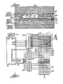
- the column lines in Fig. 5 correspond to the conductors 70-77 in Fig. 1, and form a grid with row lines in Fig. 5 that correspond to the conductive tracks 14-17 and 14a-17a in Fig. 1.
- the row lines are connected to ground through a set of resistors 103, so that when current is present at the sense points 104 in Fig. 5, it will flow through the resistors 103 to provide voltages across the inputs of two 4-unit packages of comparators 105, 106.
- Quad packages of LM339 comparators available from National Semiconductor Corp., Santa Clara, California, are suitable for use as the comparators 105, 106.
- Each individual comparator converts an analog, capacitive signal generated from one of the capacitive switches to a logic level signal that can be read by the microcomputer 100.
- the comparators 105,106 are always active, so that a signal at any of the sense points 104 is available on one of the lines in the data bus 107 that couple the sense data to the microcomputer 100.
- the increased capacitance will cause current flow and will generate a voltage of approximately +5 DC volts at the input to one of the comparators 105, 106. Similar input voltages will also be generated for others of the comparators 105,106 for each switch in the column that is actuated. The input voltages will appear on the row lines at the sense points 104, and will exceed the 175-millivolt threshold voltage needed to switch the outputs of the comparators. The input voltage signal will then decay as the capacitive switch charges-at a rate determined by the RC time constant for each individual switch circuit.
- the voltage across the comparator input will drop below the switching threshold and the output of the comparator will switch back to its original state.
- the time period that the comparators are switched is long enough in this instance to allow the microcomputer 100 to read the changed state of the comparator outputs as representing the actuation of various switches in the matrix.
- the microcomputer 100 executes instructions to drive the column lines and to read the row lines, it executes further instructions to discharge the array of capacitance switches. This produces a control signal from the microcomputer 100 that is transmitted to an inhibit (INH) input on the latch/decoder 102. This will ground the outputs of the latch/decoder 102, allowing the capacitive switches to discharge.
- IH inhibit
- the membrane switch 1 that has been described herein provides a capacitance switch array that will be useful in micro electronic equipment.
- the capacitance membrane switch 1 can be utilized in any industrial application in which a membrane switch is a desirable element.
- the present capacitance switches will generally exhibit a longer life that can be useful in various applications. They also have the capability of providing "n" key rollover when decoded in large matrix arrays. This means that the open or closed condition of any switch position in a matrix can be electronically detected regardless of the condition of all other switch positions.
- Typical installations for a capacitance membrane switch 1 are as a switch element of a full travel keyboard to provide a data entry keyboard that can be used with a computer, typewriter, calculator keyboard and the like. Also, the capacitance membrane switch 1 can be used as a control switch for appliances such as microwave ovens and stoves, or as a control panel for various types of instruments.
- the switch 1 in the specific embodiments described above comprises a flexible film layer having a lower surface carrying a conductive pattern, a dielectric film layer having upper and lower surfaces, and a second layer having an upper surface carrying a conductive pattern, first spacer means between the lower surface of the flexible film layer and the upper surface of the dielectric film layer and second spacer means between the lower surface of the dielectric film layer and the upper surface of the second layer.
- the switch includes first capacitor plates on the lower surface of the flexible film layer, second capacitor plates on the upper surface of the dielectric film layer, and third capacitor plates between the lower surface of the dielectric film layer and the second layer, to thereby provide at least one switch array, preferably a plurality of switch arrays, each including first, second and third capacitor plates arranged so as to provide a variable capacitor between the first and second capacitor plates and a fixed capacitor between the second and third capacitor plates.
- the third capacitor plates are to consist of conductive adhesive bonded to the lower surface of the dielectric film layer and bonded to the upper surface of the second layer comprising conductive particles distributed within a polymeric binder matrix and developing an electrically conductive path through the binder matrix.
- the conductive adhesive operates electrically as a capacitor plate in the switch, operates mechanically to bond together portions of the dielectric film layer and the second layer, and operates electrically to form a conductive interface with the conductive pattern on the upper surface of the second layer.
- a conductive adhesive layer to provide the foregoing characteristics has numerous advantages for the construction of a capacitance membrane switch.
- this type of switch it is desirable to generate high capacitance for the fixed capacitor element of the switch, which, in turn, requires the use of a thin dielectric film which may be only about 0.0025 to 0.0125 mm thick. It can be appreciated that printing capacitor plates on a film as thin as this would be very difficult and perhaps economically unfeasible.
- a conductive adhesive layer as described above enables a manufacturer to apply the conductive adhesive layer in the required pattern on an upper surface of the second layer, such as the layer 10 described above, laminate the very thin dielectric film layer to the second layer by means of, in part, the conductive adhesive layer, and thereafter print second capacitor plates on the exposed first surface of the dielectric film layer.
- conductive adhesive for the third capacitor plates gives the manufacturer a great deal of flexibility with respect to the location and configuration of the third capacitor plates in comparison, for example, to vapor deposition metalization techniques employed in certain prior art for forming capacitor plates. Also, there is a reduction of both the number and the complexity of the manufacturing operations that have to be performed on a very thin film such as the dielectric film layer. As noted, the need to print capacitor plates on a thin unsupported dielectric film layer has been eliminated, and there is also a reduction in steps such as slitting thin film into narrow strips as in some prior constructions.
- the conductive adhesive construction of the present invention provides for enhanced support of the dielectric film layer in a mechanical sense due to its adhesion thereto and also in an electrical sense since electrical contact can be distributed over a substantially large area.
- the use of a conductive adhesive layer in the manner disclosed provides significant flexibility in keyboard design or layout since connection with the dielectric layer can take place anywhere along the layer, thereby reducing spatial limitations in capacitance switch designs.
Landscapes
- Push-Button Switches (AREA)
- Switches That Are Operated By Magnetic Or Electric Fields (AREA)
- Electronic Switches (AREA)
- Oscillators With Electromechanical Resonators (AREA)
- Electrophonic Musical Instruments (AREA)
- Electrostatic, Electromagnetic, Magneto- Strictive, And Variable-Resistance Transducers (AREA)
Abstract
Description
- This invention relates to electrical switches of the type having movable contacts disposed on a flexible plastic film, i.e. membrane switches according to the first part of
claim 1. - The term membrane switches is generally used to refer to electrical switches constructed of two or more spaced layers of plastic film carrying conductive zones, areas or electrodes that are typically printed on the film with conductive inks. One film is arranged to be flexed or depressed toward another so as to establish an electrical circuit between specific electrodes thereby generating a signal that can be detected by external circuitry to which the membrane switch is connected. The term membrane switches is also used in reference to switches having a single flexible plastic film of the foregoing type in combination with a rigid substrate or layer, each carrying conductive zones, areas or electrodes.
- Membrane switches have become significant articles of commerce within approximately the last decade, and presently find widespread use in installations in which a sealed or protected switch or operating panel is a desirable component. Thus, membrane switches find use in equipment which requires manual data entry such as computer keyboards, terminal, cash registers and the like. Also, membrane switches are widely used as a control or instrument panel for appliances such as washers and microwave ovens, industrial controls, copy machines, and the like, in which a finger touch micro-motion actuation is a useful feature.
- Membrane switches are actuated simply by an operator depressing, with a finger, a selected or designated area of one layer of the switch towards another layer, the two layers being closely spaced from one another layer, the two layers being closely spaced from one another so that only a slight amount of movement of the layer which is depressed is required for proper operation.
- Membrane switches have been primarily of the resistance type in which two contacts are closed and electric current flows through them in proportion to the voltage applied across them. Resistance switches are well known in the art and particular constructions for this type of membrane switch are disclosed in a number of patents including e.g., U.S. Patents 4,217,473, 4,218,600 and 4,264,797.
- A more recent development on the art of membrane switches is the capacitance type of membrane switch which operates upon the change of capacitance between spaced electrodes or contacts. In a capacitance membrane switch, a first set of capacitor plates or contacts is formed as a conductive pattern on the underside of a first film layer. A dielectric film layer is spaced from the first film layer and second and third capacitor plates are located on either side of the dielectric film layer. Assuming the second capacitor plates face the first capacitor plates on the underside of the first film layer, a variable air capacitor is established between the first and second capacitor plates and a fixed capacitor is established between the second and third capacitor plates, with the variable and fixed capacitors being in series with one another. When the conductive pattern on the underside of the first film layer and the third capacitor plates are connected to external circuitry, a detectable change in capacitance is developed when the first layer is depressed to establish contact between the conductive pattern on its underside and the second capacitor plates. Capacitance membrane switches of this general type are described in U.S. patent 4,367,385 and U.S. patent 4,359,720.
- According to U.S. patent 4,433,223 conductive adhesive have been used already in membrane switches for their electric and bonding properties.
- It is the object of the invention to provide a novel structure for capacitance membrane switches that would result in an improved switch construction and facilitate the manufacture of capacitance membrane switches.
- According to the present invention this object is solved by the features of the second part of
claim 1. - The present invention is described by reference to the accompanying drawings in which:
- Fig. 1 is an exploded view of a capacitance membrane switch constructed in accordance with this invention;
- Fig. 2 is a sectional view of the capacitance membrane switch of Fig. 1 taken along the plane of line 2-2 of Fig. 3;
- Fig. 3 is a perspective view of the capacitance membrane switch of Fig. 1, with portions broken away to further clarify its structural details;
- Fig. 4 is an enlarged sectional view of a portion of the capacitance membrane switch of Fig. 1 taken along the plane of line 4-4 of Fig. 3; and
- Fig. 5 is an electrical schematic diagram of the capacitance membrane switch of Fig. 1 and associated decoding circuitry.
- The following description is arranged in three parts to facilitate a full understanding of the present invention; (1) structural description, including specific examples, (2) electrical description, which explains the operation of the capacitance membrane switch of this invention, and (3) industrial applicability, setting forth a number of significant advantages of the new capacitance membrane switches and typical uses for the switches.
- Fig. 1 is an exploded view of an exemplary form of a capacitance membrane switch according to this invention identified by the
general reference numeral 1 in which the various layers of the switch are separated from one another for clarity of description, it being understood that the layers are joined together to form the assembled switch as shown in Figs. 2 and 3. Each layer of theswitch 1 is explained in subsections (a)-(f) below by reference to Fig. 1, starting with the lowermost layer shown in the drawing. - (a)
First layer 10 of theswitch 1 is illustrated as a layer of suitable flexible plastic film, and is shown as a general rectangular element, although it can be any specific shape for a particular application. A tail 11 extends from one side of thelayer 10, for the purpose described below. Aconductive pattern 12 is carried on theupper surface 13 of thelayer 10 and comprises a plurality of spaced parallel longitudinal conductive tracks 14-18 and a plurality of conductors 20-28.Conductive tracks layer 10. Conductive tracks 15 and 15a are arranged in an end-to-end relationship with each other and slightly spaced from one another; the pairs of conductive tracks 16 & 16a and 17 & 17a are arranged in a similar fashion.Conductive track 18 is a shorter longitudinally-aligned conductive track spaced outwardly oftrack 14.Conductor 20 extends from near an end ofconductive track 14 first transversely across thelayer 10, next longitudinally along thelayer 10, and thereafter transversely along the tail 11. In a similar fashion,conductors conductive tracks 14a, 15, 15a, 16 and 16a respectively and along the tail 11. Conductor 26 extends from near an end ofconductive track 17 first longitudinally along thelayer 10 and then transversely along the tail 11, andconductor 27 extends transversely of thelayer 10 and along the tail 11 from near an end ofconductive track 17a.Conductor 28 connectsconductive track 18 toconductive track 14 as illustrated. - The particular form of the
conductive pattern 12 on the surface of thelayer 10 is not a part of the present invention, and the conductive pattern can be of any style suitable for a particular switch design or application and may for example, comprise a plurality of conductive areas or pads connected to conductors extending onto the tail of the layer. - As to materials, the
layer 10 can be made of any nonconductive flexible plastic film suitable for membrane switches: polyester films, such as polyethylene terephthalate films, are the most commonly used materials, although, polycarbonate films, polyimide films and polysulfone films, as well as others such as polyolefin and unplasticized polyvinyl chloride films, may be used. The film can be in the range of about 0.025 to 0.375 mm thick, or thicker if so desired, with 0.125 mm thick films being preferred as providing physical properties appropriate to most membrane switch applications at a reasonable cost. Also, however, thelayer 10 can be a rigid element, such as a layer of circuit board material, plastic or other non-conductive material. - The
conductive pattern 12 can be printed onto thesurface 13 of thelayer 10, such as by screen printing suitable conductive inks containing silver, gold, copper, carbon or graphite or other appropriate metal powders dispersed in a suitable binder to form the selected pattern. Many suitable conductive inks are known in the art and are commercially available. Also, however, the conductive pattern can be formed by vacuum deposition of conductive metals such as silver, gold, aluminum or copper onto the surface of thelayer 10, as well as by etching techniques or by plating techniques. - (b) Nonconductive
adhesive layer 30 is the next element of theswitch 1 and is formed in the same size and shape as thelayer 10, including a tail 31 at the same location as tail 11. Tail 31 is about 6 mm shorter than tail 11 of thelayer 10 so as to leave an exposed end portion of tail 11 for attachment to a connector.Adhesive layer 30 is shown as a patterned layer including four parallel, spacedelongated apertures 34, 35, 36, and 37 extending longitudinally across most of the length of the layer and a shorter aperture 38 positioned outwardly of apertures 34 and parallel thereto as shown. In the assembled switch as illustrated in Figs. 2 and 3, theadhesive layer 30 is adhered to and covers thesurface 13 oflayer 10 except for the portions of thesurface 13 within the apertures 34-38 and at the end of the tail 11. - The
adhesive layer 30 is to function as an assembly adhesive joining thelayer 50 to be described in part (d) below to thelayer 10, and may comprise a layer of heat activated adhesive, thermoset adhesive, or pressure sensitive adhesive. Many suitable adhesives are well known in the art, and a particular adhesive should be selected with regard to the specific materials employed for thelayers adhesive layer 30 may be of any selected thickness, with a thickness in the range of about 0.001 to 0.125 mm being suitable for most membrane switch constructions, although the layer can be thicker if so desired. - (c) The next element of the
switch 1 is a conductive adhesive layer 40 which, in the exemplary embodiment, comprises a plurality of spaced blocks or zones of adhesive 44 & 44a, 45 & 45a, 46 & 46a, 47 & 47a and 48 arranged as shown in Fig. 1. In the assembled switch, illustrated in Figs. 2 and 3, the blocks orzones 44 & 44a of the conductive adhesive layer are positioned in the aperture 34 ofadhesive layer 30;blocks 45 & 45a of the conductive adhesive layer are positioned within the aperture 35 ofadhesive layer 30;blocks 46 & 46a of the conductive adhesive layer are positioned within theaperture 36 of theadhesive layer 30; andblocks 47 & 47a of the conductive layer are positioned within the aperture 37 of theadhesive layer 30. Similarly, block 48 of the conductive adhesive layer is positioned within the aperture 38 of theadhesive layer 30. This arrangement is depicted in Fig. 3 whereinblock 47 of the conductive adhesive layer 40 is positioned within aperture 37 of theadhesive layer 30, andblock 46 is positioned withinaperture 36 of theadhesive layer 30. - The conductive adhesive layer 40 is an essential element of the present invention, and its functionality in the switch construction and suitable compositions are described below in greater detail in part (h) hereof. The conductive adhesive layer 40 is to be of about the same thickness as the
adhesive layer 30, or preferably somewhat thicker for the reason described in part (h). - (d) The next element of the
switch 1 is adielectric film layer 50 of the same shape and size of thelayer 10.Dielectric film layer 50 includes a tail 51 of the same size and shape as tail 31 oflayer 30 and will be superimposed thereon in the assembled switch. A plurality ofcapacitor plates 52 are carried on the upper surface 53 of thelayer 50. Thecapacitor plates 52 are arranged in a first row 54, a second row 55, a third row 56 and a fourth row 57 thereof. The rows 54-57 extend longitudinally along thedielectric film layer 50 and are parallel to but spaced from one another. Thecapacitor plates 52 are arranged in generally column form among the rows 54-57. A separate capacitor plate 58 is spaced from the first row 54 of thecapacitor plates 52 on the upper surface 53. - The
dielectric film layer 50 is to comprise a layer of flexible plastic film, such as polyester film, (generally polyethylene terephthalate film), polycarbonate film, polyvinyl fluoride film, polyvinylidene fluoride film, or polyolefin film. Suitable materials are available commercially from a number of companies, including Dupont and General Electric. Since thelayer 50 is to form the dielectric layer of a capacitance element, as explained in detail in part (2) below, it is preferable that the layer be quite thin so as to provide for high capacitance; for this reason, capacitor grade plastic films of about 0.0025 to 0.125 mm thick are generally most useful, with a film about 0.006 to 0.0125 mm thick preferred for most switch applications. - The
capacitor plates 52 and 58 can be applied to the surface 53 of the dielectric layer by any appropriate technique. A useful technique is to print theplates 52 and 58 onto the dielectric layer by screen printing techniques utilizing conductive inks such as those including silver, graphite, carbon, copper or gold metal powders in a suitable binder. Theplates 52 and 58 may also be applied by vacuum deposition of metals such as silver, gold, aluminum or copper onto the surface of the film or by plating techniques. As was the case with theconductive pattern 12 on thefirst layer 10, the array ofcapacitor plates 52 and 58 can be applied in patterns other than that illustrated in Fig. 1. - (e) The uppermost element of the
switch 1 as illustrated in Fig. 1 is aflexible film layer 60 of plastic film, which is of the same size aslower layer 10. A tail 61 extends from one side of thelayer 60 that is offset longitudinally relative to the tail 11 of thelower layer 10. An upperconductive pattern 62 is carried on thebottom surface 63 of thelayer 60. Thepattern 62 includes a plurality ofcapacitor plates 64 arranged in column-portions of four each in a first row 66 extending longitudinally across thelayer 60, a secondlongitudinal row 67, thirdlongitudinal row 68 and fourthlongitudinal row 69 thereof. A capacitor plate 65 is positioned outwardly of the first row 66 of thecapacitor plates 64. Thecapacitor plates 64 are connected byconductors plates 64 to form a column of eightcapacitor plates 64 electrically connected together and has a portion extending along the tail 61 as shown in Fig. 1. Thus,conductor 71 interconnects the left hand column-portion A ofcapacitor plates 64 and the right hand column-portion B ofplates 64 as shown in Fig. 1, and conductor 73 interconnects the next innermost column-portions C and D ofplates 64. Theother capacitor plates 64 and capacitor plate 65 of thepattern 62 are connected to other of theconductors 70, 72 and 74-77. - The
conductive pattern 62 illustrated in Fig. 1 would typically be used with a computer input keyboard that includescapacitor plates 64 in a left hand array E andcapacitor plates 64 in a right hand array F. Array F includescapacitor plates 64 for the actuating keys of a typical qwerty typewriter keyboard, and array E includesplates 64 for calculator keys as part of the keyboard; capacitor plate 65 would be for a space key of the keyboard. Any selected pattern for the upperconductive pattern 62 can be used for theswitch 1, depending upon the intended use for the switch, however, and thespecific pattern 62 illustrated in the drawings is not part of the present invention. - The
flexible film layer 60 can be made of any non-conductive flexible plastic film suitable for membrane switches. Polyester films, particularly polyethylene terephthalate films, are most commonly used, although polycarbonate films, polyimide films and polysulfone films, as well as others such as polyolefin and unplastisized polyvinyl chloride films, may be used. Thefilm 60 can be in the range of about 0.05 to 0.5 mm thick and should be thick enough so that it will maintain its spacing from thefirst layer 10; the specific film chosen for a particular application will depend in part upon the amount of force for actuating the switch selected by the designer. Afilm 60 of about 0.125 mm thick is suitable for most membrane switch applications. The upperconductive pattern 62 is to adhere to thebottom surface 63 of thefilm 60 and it may be applied thereto by the same techniques and materials described above in part (a) in connection with theconductive pattern 12, i.e., screen printing with conductive inks, vacuum deposition, etching or plating techniques. - (f) A spacer layer 80 is interposed between the
flexible film layer 60 and thedielectric film layer 50. In the embodiment of Fig. 1, the spacer layer 80 includes anupper stratum 81 and alower stratum 82. Theupper stratum 81 comprises a coating of ultraviolet light curable material which is coated onto and adhered to thebottom surface 63 of theflexible layer 60; it is shown in Fig. 1 as being separate from thelayer 60 for clarity of description. Theupper stratum 81 includes a tail portion 81 a which is of the same location and shape as the tail 61 of thelayer 60 but is about 6 mm shorter to leave an exposed end portion of tail 61 for attachment to a connector. Thelower stratum 82 is a layer of pressure sensitive adhesive. - The
stratum 81 of the spacer layer 80 includes a plurality ofapertures 84 that extend through the entire thickness of the stratum and are slightly larger in size than thecapacitor plates 64 of the upperconductive pattern 62 of thelayer 60 and an aperture 85 that is slightly larger than capacitor plate 65 thereof. In the assembled switch, oneaperture 84 is arranged underneath eachplate 64 and aperture 85 is underneath plate 65. Theapertures 84 are arranged in fourparallel rows 86, 87, 88 and 89. A longitudinal plenum channel 90 extends through thestratum 81 and is located between rows 86 and 87 of theapertures 84. Alongitudinal plenum channel 91 also extends through thestratum 81 and is positioned betweenrows 88 and 89 of theapertures 84.Plenum channels 90 and 91 are each connected to avent channel 93, also formed as an aperture extending through the entire thickness of thestratum 81. Aperture 85 is connected to plenum channel 94 that extends to ventchannel 93. - The
stratum 82 of the spacer layer 80 includes a plurality of apertures 84' that are the same size asapertures 84 of thestratum 81. Apertures 84' extend through the entire thickness of thestratum 82. There is one aperture 84' in thestratum 82 for eachaperture 84 of thestratum 81, so that in the assembled switch there will be an aperture 84' under eachaperture 84. The apertures 84' of thestratum 82 are arranged in four parallel rows 86', 87', 88' and 89'. The apertures 84' of the row 86' and the apertures 84' of the row 87' are connected to a longitudinal manifold channel 90' by connecting channels 95, and the apertures 84' of the rows 88' and 89' are connected to a longitudinal manifold channel 91' by similar connecting channels 95. The manifold channels 90' and 91' are located underneath and in registry with thelongitudinal plenum channels 90 and 91 of thestratum 81 in the assembled switch. Manifold channels 90' and 91' are each connected to vent channel 93' which underlies and is in registry with thevent channel 93 of thestratum 81. Thestratum 82 also includes a channel 94' that connects an aperture 85' which underlies and is in registry with aperture 85 of thestratum 81, to the vent channel 93'. - The
vent channels 93 and 93' extend to an outer edge of the spacer layer 80 and are employed to equalize internal air pressure built up betweenflexible film layer 60 anddielectric film layer 50 with the external atmospheric pressure so as to permit proper actuation of theswitch 1. For example, excess air pressure within the registeredapertures 84 and 84' of the assembled switch will be vented through manifold channels 90' or 91', and their associated superimposedplenum channels 90 and 91, throughvent channels 93 and 93' and to the atmosphere. - The spacer layer 80 is of a thickness appropriate to maintaining the
flexible film layer 60 out of contact with thedielectric film layer 50; for most switch applications, a spacer layer in the range of about 0.0375 to 0.25 mm thick is appropriate. Also, however, the spacer layer should not be so thick as to prevent thecapacitor plates 64 from being depressed into contact with thecapacitor plates 52 on the upper surface of thedielectric film layer 50 when the switch is to be operated. Many types of coatings can be used for thestratum 81 of the spacer layer such as ultraviolet curable coatings, solvent coatings of thermoplastic resins such as acrylics and polyesters or thermoset resins such as urethanes and epoxies. Any coating that can be applied in the requisite thickness may be used. Also, instead of thecoating 81 and adhesive 82 strata, the spacer layer 80 can be made of a layer of plastic film with adhesive on both of its surfaces, or it may be a single thick layer of adhesive. Further, although illustrated as pressure sensitive adhesive, thestratum 82 of the spacer layer may be made of heat activated adhesive or thermoset adhesive. To manufacture theswitch 1, thestratum 81 when comprising a coating is first coated onto thebottom surface 63 of theflexible film layer 60, and then theadhesive layer 82 is applied over the coating ofstratum 81. - (g) The
capacitance membrane switch 1 in its assembled condition is illustrated in sectional view in Fig. 2 and perspective view in Fig. 3, which should be referred to for the following description. - The non-conductive
adhesive layer 30 is adhered to theupper surface 13 of thelower layer 10 and the lower surface 59 of thedielectric film layer 50 so as to firmly bond thelayers conductive track 14 of theconductive pattern 12 on the upper surface of thelayer 10 is positioned within and slightly spaced from a side edge of aperture 34 of theadhesive layer 30 andconductive track 14a is positioned within aperture 34 along an opposite side edge thereof. Conductive tracks 15 and 15a are positioned within and near an edge of aperture 35 of the non-conductiveadhesive layer 30, conductive tracks 16 and 16a are positioned within and near an edge ofaperture 36 of theadhesive layer 30;conductive tracks conductive track 18 is positioned within and near an edge of aperture 38 of theadhesive layer 30. The remaining portion of theconductive pattern 12 is covered by the non-conductiveadhesive layer 30. - ' The conductive adhesive layer 40 is positioned within the apertures 34-38 of the non-conductive
adhesive layer 30 so that its several elements cover conductive tracks 14-18.of thepattern 12. Turning first to Fig. 3, it will be noted thatblock 47 of the conductive adhesive layer 40 is positioned within aperture 37 of the non-conductiveadhesive layer 30 and coversconductive track 17; also, block 46 of the conductive adhesive layer 40 is located withinaperture 36 oflayer 30 and covers conductive track 16 of thepattern 12. Thus, in the assembled switch, blocks 44 and 44a of the conductive adhesive layer 40 are located within aperture 34 of the non-conductiveadhesive layer 30 and cover, respectively,conductive tracks pattern 12;blocks layer 30 and cover, respectively, conductive tracks 15 and 15a; blocks 46 and 46a of the conductive adhesive layer 40 are located withinaperture 36 oflayer 30 and cover, respectively, conductive tracks 16 and 16a; blocks 47 and 47a of layer 40 are located within aperture 37 oflayer 30 and cover, respectively, tracks 17 and 17a; and block 48 of the layer 40 is located within aperture 38 oflayer 30 and coversconductive track 18. This relationship is illustrated in Fig. 2 with respect toblocks - As previously described, the non-conductive
adhesive layer 30 serves to bond together thedielectric film layer 50 and thelower layer 10. Also, however, the conductive adhesive layer 40 is joined to both theupper surface 13 of thelower layer 10 and the bottom surface 59 of thedielectric film layer 50 to additionally bond together thelayers adhesive layer 30 by reason of the apertures 34-38 therein. - Further, the conductive adhesive layer 40 is arranged to underlie the capacitor plates 52 (see Fig. 2) and 58 carried on the top surface 53 of the
dielectric film layer 50. The first row 54 ofcapacitor plates 52 are positioned above theblocks 44 and 44a of layer 40 in the assembled switch; the second row 55 ofcapacitor plates 52 are positioned aboveblocks capacitor plates 52 are positioned aboveblocks capacitor plates 52 are positioned aboveblocks - The
adhesive stratum 82 of the spacer layer 80 is bonded to the top surface 53 of thedielectric film layer 50 and serves to join theflexible film layer 60 thereto in the completedswitch 1 inasmuch as theupper strata 81 of the spacer layer 80 is, as previously described, coated onto thebottom surface 63 of thelayer 60. Theapertures 84 and 84' of the spacer layer 80 are arranged in registration with thecapacitor plates 52 of thedielectric film layer 50 and aperture 85 of spacer layer 80 is arranged in registry with capacitor plate 58 offilm layer 50. The first row 86 and 86', respectively, ofapertures 84 and 84' of the spacer layer are positioned such that there is anaperture 84 and 84' positioned over eachcapacitor plate 52 of the first row 54 thereof; similarly, anaperture 84 and 84' of therows 87 and 87', 88 and 88' and 89 and 89' are positioned, respectively, above aplate 52 of the rows 55, 56 and 57 thereof. Apertures 85 and 85' of the spacer layer 80 are positioned above capacitor plate 58. - (h) The conductive adhesive layer 40 is considered to be the primary novel feature of the present invention in comparison to prior technology relating to capacitance membrane switches. As explained above, the conductive adhesive layer functions both electrically and mechanically in the
capacitance switch 1, which is a significant departure from known capacitance membrane switch constructions. The conductive adhesive layer 40 comprises two principal ingredients: (1) conductive particles and (2) a resinous binder. - Conductive particles suitable for the conductive adhesive layer include silver, gold, copper, carbon and graphite particles. Silver particles provide excellent conductivity for the adhesive layer 40, but graphite particles are particularly useful since they provide very good conductivity at an economical cost. The conductive particles are to be distributed throughout the resinous binder of the conductive adhesive layer, i.e. they are distributed relatively uniformly within the binder as distinguished from being present as a stratified layer within the binder. The conductive particles are to be dispersed throughout the binder in "electrically touching" distribution, which term as used herein and in the claims is defined as meaning the conductive particles touch one another or are separated from one another by a small enough distance so that they provide an electrically conductive path through the conductive adhesive layer.
- The binder for the conductive adhesive layer forms the resinous matrix within which the conductive particles are distributed and also acts as the material bonding together the two elements joined by the conductive adhesive layer, namely
dielectric film layer 50 andlayer 10 of thecapacitance switch 1. The binder is to comprise a polymeric resinous material, with the particular binder selected for the conductive adhesive layer for a specific switch being dependent largely upon the composition of thelayers layers dielectric layer 50 so that there will be no or very little air entrapped between the adhesive-film interface which would alter the capacitance of each fixed capacitor of the switch. Thus, the binder should exhibit a high level of wet-out of thelayer 50 and achieve consistent contact therewith so that the capacitance of the fixed capacitance switch areas will not fluctuate to a significant degree. Various resins can be used as the binder of the conductive adhesive layer including, for example, amine cured liquid epoxy resins, polyaziridine cured carboxy functional acrylic resins, heat activated polyester resins, silicone resins, urethane resins, melamine cured polyester resins, ultraviolet curable acrylate resins and the like. Silicone resins are the binder of choice when one or the other of thelayers layers - The conductive adhesive layer can be a heat activated adhesive, pressure sensitive adhesive, thermosetting adhesive, room temperature curable adhesive, or ultraviolet curable adhesive. Heat activated and thermosetting adhesives are considered especially useful since the addition of conductive particles appears to have less deleterious effect on the adhesion on these types of adhesives to the layers. The addition of conductive particles to pressure sensitive adhesives can make it more difficult to get sufficient flow of the adhesive to obtain good bonding at theadhesive-layer interfaces, but useful pressure sensitive adhesives can be formulated for the conductive adhesive layer. The conductive adhesive can be formulated as a solvent solution or hot melt composition, depending upon the type of equipment selected to apply the adhesive. A coatable solvent solution suitable for the conductive adhesive layer may include conductive particles, resinous binder, a curing agent as required for the binder, a solvent or solvents appropriate for the binder, and a defoaming agent. The solvent system should have an evaporation rate compatible with the application and drying equipment to be used.
- The conductive adhesive layer 40 preferably is at least as thick as the nonconductive
adhesive layer 30 which surrounds it, as described above. Thus, a conductive adhesive layer of about 0.0025 to 0.125 mm thick is suitable for most membrane switch constructions, although the layer may be thicker if so desired. In general, it is preferable to apply the conductive adhesive layer at a slightly greater thickness than that of the nonconductiveadhesive layer 30 in order to ensure intimate contact between the conductive adhesive and the two layers to which it is to bond, especially with thedielectric film layer 50. The conductive particles admixed with the resinous binder in the conductive adhesive layer should have a particle size that is less than the thickness of the conductive adhesive layer; if the conductive particles are larger than the thickness of the conductive adhesive layer, they could project slightly from the surfaces of the conductive adhesive layer and thereby impair the bonding of the surfaces to thedielectric film layer 50 and thelayer 10 of the switch. In general, again depending upon the thickness of the conductive adhesive layer, conductive particles with a particle size in the range of less than 10 microns will be suitable. - Several representative formulae for the conductive adhesive layer are set forth below. All three formulae have been tested and proven to be useful in a capacitance membrane switch as described above, with
Formula 1 being the preferred composition at the present time. -
Formula 1 is based upon an isocyanate cured low molecular weight polyester binder, a viscous liquid of 90% solids content, and graphite for the conductive particles. The several ingredients are mixed together in a ball mill to prepare the composition. The conductive particles were about 50 microns in diameter prior to milling, and were estimated to be less than 10 microns in diameter after milling. -

-
Formula 2 employs an isocyanate cured acrylic resin as a binder and a mixture of graphite and carbon particles for the conductive particles. The composition was processed in the same manner asFormula 1, and the conductive particles size was estimated at less than 10 microns after ball milling. -

- Formula 3 is an example of a pressure sensitive adhesive suitable for the conductive adhesive layer which is based upon an acrylic binder and carbon particles as the conductive particles. The ingredients except for the acrylic resins were mixed by ball milling, following which the acrylic resins were added. The size of the conductive particles was estimated to be about 10 microns or less in the finished composition.
-

- The conductive adhesive material can be applied to the
layer 10 of the switch by any suitable manner. Screen printing has proved useful, particularly when the conductive adhesive layer is in the form of several spaced blocks such as described above in part (c). The specific application technique will depend, at least in part, upon the composition of the conductive adhesive and the configuration of the conductive adhesive layer. - The conductive adhesive layer 40, as described previously, is to function as one of the capacitor plates of the fixed capacitor of the
switch 1 and also provide an electrical interface with a conductive pattern on the surface of thelayer 10 to which it is bonded. The conductive adhesive layer should have a maximum sheet resistance of about 50 kiloohms/square, or lower. The sheet resistance of the conductive adhesive layer can be varied as required for a specific switch. Also, the sheet resistance of any specific conductive adhesive layer should be related to the frequency of any scanning circuit employed in combination with the capacitance switch. For systems operating at a relatively low frequency, such as about 100 Hertz as a sample frequency, the sheet resistivity of the conductive adhesive can be at the higher end of about 50 kiloohms/square; however, if the scanning circuit operates at a higher frequency, the sheet resistivity of the conductive adhesive layer should be regulated by the proportion of the conductive particles therein so as to have a lower sheet resistivity than this upper limit such as about 3 kiloohms/square or less. Also, the conductivity of the conductive adhesive layer can be augmented, if considered necessary when the switch is to be used with high frequency scanning circuits such as about 1 megaHertz, by increasing the area of theconductive pattern 12 under the conductive adhesive layer. - When the
flexible film layer 60 andstratum 81 of the spacer layer 80 in Fig. 1 are joined byadhesive stratum 82 to the top of the sandwich oflayers capacitor plates 64 in Fig. 1 are in registry with theapertures 84 and 84' of spacer layer 80 and thecapacitor plates 52 onlayer 50. The assembled layers form an array of capacitive switches, one of these switches being seen in detail in Fig. 4. - Fig. 4 illustrates a
capacitor plate 64 connected toconductor 71 that runs along the underside of theflexible film layer 60. Theapertures 84 and 84' in the spacer layer 80 provide an air gap between thecapacitor plate 64 and its underlying thecapacitor plate 52, and forms, in effect, a variable capacitor (represented in phantom). This variable capacitor uses air as its dielectric, and is variable due to the ability ofcapacitor plate 64 to move downward and engagecapacitor plate 52. When this occurs, the air gap is no longer present and theplate 64 and theplate 52 act as a conductor rather than as a capacitor. - The
plate 52 and the block of conductive adhesive 47 form the upper and lower plates, respectively, of a fixed capacitor element (represented in phantom) that utilizes a portion oflayer 50 as its dielectric. The conductive adhesive 47 contacts track 17 fortransmission of a sense signal through thetrack 17 in response to a drive signal applied throughconductor 71 to plate 64,air gap 84,plate 52,dielectric 50 andconductive adhesive 47. These elements are connected in series in a circuit path formed between theconductor 71 carrying the drive signal andconductors 16, 17 which carry the sense signals. If one of the capacitive switches is being operated by depressinglayer 60, the variable capacitor is removed and only the fixed capacitor is effective in the switch circuit. This produces greater charge at theplates tracks 16, 17 that produces the sense signals. - In forming the lower plate of a fixed capacitor, the
conductive adhesive 47 is performing one of its three functions. It also functions as a bonding agent forlayers - Also seen in Fig. 4 is a portion of neighboring capacitive switch that includes a
capacitor plate 52 and a neighboring block of conductive adhesive 46 formed over conductive track 16. A sense signal for this neighboring switch is transmitted through the track 16. In between the two switches, avent 91―91' formed by the spacer layer 80 is seen, as well as a portion ofadhesive layer 30 that separates conductive adhesive blocks 46 and 47. - Referring now to Fig. 5, the decoding circuitry which is connected to the
switch array 1 is controlled by amicrocomputer 100, which in this embodiment is preferably a Model 8748 microcomputer with on-board memory available from Intel Corporation, Santa Clara, California. Aclock circuit 101 that generates the base timing signals for themicrocomputer 100 is connected to its XTAL1 and XTAL2 inputs. Details of the architecture, operation and instruction set for the microcomputer are available in commercial literature from the manufacturer, and particularly the MCS-48 Microcomputer Users Manual, published in T976, and updated versions thereof. Themicrocomputer 100 has two 8-bit I/O ports, and four terminals (P20-P23) in one of these I/O ports are connected to transfer four drive signals to a 4-bit Iatch/ 1-of-16decoder 102. Such a decoder is available under part designation CD4514B from RCA Corporation, Somerville, New Jersey. Thiscircuit 102 receives, holds, and decodes four bits of information received from themicrocomputer 100 and then enables one of the sixteen columns in theswitch matrix 1 by generating an output signal, referred to herein as a drive signal. It will be noted with reference to Fig. 1 that only eight column conductors 70-77 have been shown. The specific embodiment shown there uses but eight of the possible sixteen columns that are available from the decoding circuitry, however, it is anticipated that other embodiments providing a 128-switch array would utilize all sixteen of the available drive signals. - The column lines in Fig. 5 correspond to the conductors 70-77 in Fig. 1, and form a grid with row lines in Fig. 5 that correspond to the conductive tracks 14-17 and 14a-17a in Fig. 1. As seen in Fig. 5, the row lines are connected to ground through a set of resistors 103, so that when current is present at the sense points 104 in Fig. 5, it will flow through the resistors 103 to provide voltages across the inputs of two 4-unit packages of
comparators comparators microcomputer 100. In this decoding circuit, the comparators 105,106 are always active, so that a signal at any of the sense points 104 is available on one of the lines in thedata bus 107 that couple the sense data to themicrocomputer 100. - Referring back to Fig. 4, when a switch is deactuated, and a
full air gap 84 is present, the application of a drive signal will result in a current of a low level and short duration that charges the air capacitor. This produces a voltage spike of short duration at the sense points 104 in Fig. 5. There is a delay of 25-30 microseconds between the generation of the drive signal and the sensing of the comparator outputs. This delay assures that the charging of the deactuated switches will not be seen by themicrocomputer 100 as the actuation of the switches. The delay is accomplished by the selection and arrangement of the instructions executed by themicrocomputer 100 to generate the drive signals, to wait for the delay period, and then to read the input data from the row lines. - On the other hand, assuming that the switch in Fig. 4 is actuated (depressed) when the drive signal is transmitted through
plate 64, the increased capacitance will cause current flow and will generate a voltage of approximately +5 DC volts at the input to one of thecomparators microcomputer 100 to read the changed state of the comparator outputs as representing the actuation of various switches in the matrix. - Each time a drive signal is transmitted on a column line such as
conductor 71 in Fig. 4, themicrocomputer 100 in Fig. 5 reads the status of eight switches in rows 1-8, respectively, which intersect that column in theswitch matrix 1. Thus, both of the neighboring capacitive switches in Fig. 4 are sensed simultaneously along with six others that are not shown there. - After the
microcomputer 100 executes instructions to drive the column lines and to read the row lines, it executes further instructions to discharge the array of capacitance switches. This produces a control signal from themicrocomputer 100 that is transmitted to an inhibit (INH) input on the latch/decoder 102. This will ground the outputs of the latch/decoder 102, allowing the capacitive switches to discharge. - From the above description, it should now be apparent that the
membrane switch 1 that has been described herein provides a capacitance switch array that will be useful in micro electronic equipment. Thecapacitance membrane switch 1 can be utilized in any industrial application in which a membrane switch is a desirable element. As compared to resistance type membrane switches, the present capacitance switches will generally exhibit a longer life that can be useful in various applications. They also have the capability of providing "n" key rollover when decoded in large matrix arrays. This means that the open or closed condition of any switch position in a matrix can be electronically detected regardless of the condition of all other switch positions. Typical installations for acapacitance membrane switch 1 are as a switch element of a full travel keyboard to provide a data entry keyboard that can be used with a computer, typewriter, calculator keyboard and the like. Also, thecapacitance membrane switch 1 can be used as a control switch for appliances such as microwave ovens and stoves, or as a control panel for various types of instruments. - The
switch 1 in the specific embodiments described above comprises a flexible film layer having a lower surface carrying a conductive pattern, a dielectric film layer having upper and lower surfaces, and a second layer having an upper surface carrying a conductive pattern, first spacer means between the lower surface of the flexible film layer and the upper surface of the dielectric film layer and second spacer means between the lower surface of the dielectric film layer and the upper surface of the second layer. The switch includes first capacitor plates on the lower surface of the flexible film layer, second capacitor plates on the upper surface of the dielectric film layer, and third capacitor plates between the lower surface of the dielectric film layer and the second layer, to thereby provide at least one switch array, preferably a plurality of switch arrays, each including first, second and third capacitor plates arranged so as to provide a variable capacitor between the first and second capacitor plates and a fixed capacitor between the second and third capacitor plates. The third capacitor plates are to consist of conductive adhesive bonded to the lower surface of the dielectric film layer and bonded to the upper surface of the second layer comprising conductive particles distributed within a polymeric binder matrix and developing an electrically conductive path through the binder matrix. The conductive adhesive operates electrically as a capacitor plate in the switch, operates mechanically to bond together portions of the dielectric film layer and the second layer, and operates electrically to form a conductive interface with the conductive pattern on the upper surface of the second layer. - The feature of a conductive adhesive layer to provide the foregoing characteristics has numerous advantages for the construction of a capacitance membrane switch. In this type of switch, it is desirable to generate high capacitance for the fixed capacitor element of the switch, which, in turn, requires the use of a thin dielectric film which may be only about 0.0025 to 0.0125 mm thick. It can be appreciated that printing capacitor plates on a film as thin as this would be very difficult and perhaps economically unfeasible. The use of a conductive adhesive layer as described above enables a manufacturer to apply the conductive adhesive layer in the required pattern on an upper surface of the second layer, such as the
layer 10 described above, laminate the very thin dielectric film layer to the second layer by means of, in part, the conductive adhesive layer, and thereafter print second capacitor plates on the exposed first surface of the dielectric film layer. This makes it relatively easy from a manufacturing standpoint to print the second capacitor plates on the dielectric film layer and eliminates the need to print third capacitor plates on its lower surface inasmuch as the conductive adhesive provides this element of the switch construction. Secondly, use of conductive adhesive for the third capacitor plates gives the manufacturer a great deal of flexibility with respect to the location and configuration of the third capacitor plates in comparison, for example, to vapor deposition metalization techniques employed in certain prior art for forming capacitor plates. Also, there is a reduction of both the number and the complexity of the manufacturing operations that have to be performed on a very thin film such as the dielectric film layer. As noted, the need to print capacitor plates on a thin unsupported dielectric film layer has been eliminated, and there is also a reduction in steps such as slitting thin film into narrow strips as in some prior constructions. Fourthly, bearing in mind that the thin dielectric film layer will be quite fragile, the conductive adhesive construction of the present invention provides for enhanced support of the dielectric film layer in a mechanical sense due to its adhesion thereto and also in an electrical sense since electrical contact can be distributed over a substantially large area. Lastly, it has been found during the development of the present invention that the use of a conductive adhesive layer in the manner disclosed provides significant flexibility in keyboard design or layout since connection with the dielectric layer can take place anywhere along the layer, thereby reducing spatial limitations in capacitance switch designs.
Claims (3)
Priority Applications (1)
| Application Number | Priority Date | Filing Date | Title |
|---|---|---|---|
| AT85105040T ATE49088T1 (en) | 1984-09-20 | 1985-04-25 | CAPACITIVE DIAPHRAGM SWITCH. |
Applications Claiming Priority (2)
| Application Number | Priority Date | Filing Date | Title |
|---|---|---|---|
| US06/652,802 US4562315A (en) | 1984-09-20 | 1984-09-20 | Capacitance membrane switch |
| US652802 | 1984-09-20 |
Publications (2)
| Publication Number | Publication Date |
|---|---|
| EP0176659A1 EP0176659A1 (en) | 1986-04-09 |
| EP0176659B1 true EP0176659B1 (en) | 1989-12-27 |
Family
ID=24618224
Family Applications (1)
| Application Number | Title | Priority Date | Filing Date |
|---|---|---|---|
| EP85105040A Expired EP0176659B1 (en) | 1984-09-20 | 1985-04-25 | Capacitance membrane switch |
Country Status (6)
| Country | Link |
|---|---|
| US (1) | US4562315A (en) |
| EP (1) | EP0176659B1 (en) |
| JP (1) | JPS6193526A (en) |
| AT (1) | ATE49088T1 (en) |
| CA (1) | CA1236895A (en) |
| DE (1) | DE3575058D1 (en) |
Families Citing this family (40)
| Publication number | Priority date | Publication date | Assignee | Title |
|---|---|---|---|---|
| JPS6170247U (en) * | 1984-10-05 | 1986-05-14 | ||
| US4689879A (en) * | 1985-01-14 | 1987-09-01 | Robertshaw Controls Company | Method of making a membrane keyboard |
| JPH064276B2 (en) * | 1985-12-10 | 1994-01-19 | ダイアホイルヘキスト株式会社 | Polyester film for membrane switch |
| JPH0529680Y2 (en) * | 1986-08-29 | 1993-07-29 | ||
| US4857684A (en) * | 1988-10-25 | 1989-08-15 | W. H. Brady Co. | Capacitance membrane switchcore with intertrace capacitive coupling and/or intratrace capacitive coupling |
| US4857683A (en) * | 1988-12-28 | 1989-08-15 | W. H. Brady Co. | Membrane switchcores with key cell contact elements connected together for continuous path testing |
| US4876461A (en) * | 1989-02-23 | 1989-10-24 | W. H. Brady Co. | Self-referencing capacitive key cell structure and switchcore matrices formed therefrom |
| US5209665A (en) * | 1989-10-12 | 1993-05-11 | Sight & Sound Incorporated | Interactive audio visual work |
| US5066937A (en) * | 1990-06-24 | 1991-11-19 | Barkley & Dexter Laboratories | Search coil assembly with laminate frame members and method for making same |
| US5423569A (en) * | 1991-07-08 | 1995-06-13 | United Technologies Automotive, Inc. | Electric signalling in a supplemental passenger restraint system |
| US5498906A (en) * | 1993-11-17 | 1996-03-12 | Staktek Corporation | Capacitive coupling configuration for an intergrated circuit package |
| US5554981A (en) * | 1994-08-31 | 1996-09-10 | Badger Meter, Inc. | Capacitive number wheel encoder for utility meters |
| US5594222A (en) * | 1994-10-25 | 1997-01-14 | Integrated Controls | Touch sensor and control circuit therefor |
| US5654615A (en) * | 1994-12-15 | 1997-08-05 | Asc Incorporated | Storage compartment sensor system for use with an automotive vehicle convertible roof |
| US5559665A (en) * | 1995-02-10 | 1996-09-24 | Eaton Corporation | Capacitive switching assembly |
| US5803748A (en) | 1996-09-30 | 1998-09-08 | Publications International, Ltd. | Apparatus for producing audible sounds in response to visual indicia |
| ES2242241T3 (en) | 1996-12-10 | 2005-11-01 | Touchsensor Technologies, L.L.C. | DIFFERENTIAL TACTILE SENSORS AND CONTROL CIRCUIT FOR THEMSELVES. |
| US7906875B2 (en) * | 1999-01-19 | 2011-03-15 | Touchsensor Technologies, Llc | Touch switches and practical applications therefor |
| US6320282B1 (en) | 1999-01-19 | 2001-11-20 | Touchsensor Technologies, Llc | Touch switch with integral control circuit |
| JP3931570B2 (en) * | 2001-02-16 | 2007-06-20 | 松下電器産業株式会社 | Manufacturing method of movable contact body |
| US7075426B2 (en) * | 2002-09-06 | 2006-07-11 | 3Si Security Systems, Inc. | Flex motion wake-up circuit for a security pack |
| FR2845216B1 (en) * | 2002-09-26 | 2005-06-03 | Arvinmeritor Light Vehicle Sys | MANUAL CONTROL FOR MOTOR VEHICLE |
| US7015407B2 (en) | 2003-12-22 | 2006-03-21 | Lear Corporation | Hidden switch for motor vehicle |
| US20050134485A1 (en) * | 2003-12-22 | 2005-06-23 | Hein David A. | Touch pad for motor vehicle and sensor therewith |
| US7180017B2 (en) * | 2003-12-22 | 2007-02-20 | Lear Corporation | Integrated center stack switch bank for motor vehicle |
| US7719142B2 (en) * | 2003-12-22 | 2010-05-18 | Lear Corporation | Audio and tactile switch feedback for motor vehicle |
| US6960735B2 (en) * | 2004-03-17 | 2005-11-01 | Lear Corporation | Multi-shot molded touch switch |
| US7208694B2 (en) * | 2004-04-16 | 2007-04-24 | Wabtec Holding Corp. | Capacitance activated switch device |
| KR100672312B1 (en) * | 2005-11-22 | 2007-01-24 | 엘지전자 주식회사 | Key Scan Dual Control Input |
| NZ571753A (en) * | 2006-04-21 | 2010-09-30 | Wabtec Holding Corp | Two-wire adapter for sensing and announcing abrupt changes in a current shunt monitor |
| US7989725B2 (en) * | 2006-10-30 | 2011-08-02 | Ink-Logix, Llc | Proximity sensor for a vehicle |
| US7898531B2 (en) * | 2006-12-27 | 2011-03-01 | Visteon Global Technologies, Inc. | System and method of operating an output device in a vehicle |
| TWM353598U (en) * | 2008-11-05 | 2009-03-21 | Darfon Electronics Corp | Membrane circuit board |
| US8503169B2 (en) * | 2009-02-18 | 2013-08-06 | American Trim, L.L.C. | Appliance control panel |
| EP2803138B1 (en) | 2012-01-12 | 2020-07-15 | Wallac OY | A method and a switch device for producing an electrical signal in response to mechanical force |
| DE102014211239A1 (en) * | 2014-06-12 | 2015-12-17 | Benecke-Kaliko Ag | Foil with integrated sensors |
| CN104201027A (en) * | 2014-07-28 | 2014-12-10 | 上海松清薄膜开关有限责任公司 | Thin film switch |
| DE102015113694B4 (en) * | 2015-08-19 | 2021-09-09 | Preh Gmbh | Capacitive control element with improved immunity to interference |
| US10084310B1 (en) * | 2016-02-08 | 2018-09-25 | National Technology & Engineering Solutions Of Sandia, Llc | Low-inductance direct current power bus |
| DE102016010971A1 (en) * | 2016-06-06 | 2017-12-07 | Preh Gmbh | Input device with two-part force sensor for actuating input and method for its production |
Family Cites Families (7)
| Publication number | Priority date | Publication date | Assignee | Title |
|---|---|---|---|---|
| US4295699A (en) * | 1969-09-15 | 1981-10-20 | Essex International, Inc. | Pressure sensitive combination switch and circuit breaker construction |
| DE2508154C3 (en) * | 1974-12-03 | 1978-06-15 | Pentel K.K., Tokio | Input plate |
| US4379287A (en) * | 1978-08-08 | 1983-04-05 | Robertshaw Controls Company | Capacitive switch and panel |
| US4367385A (en) * | 1981-01-26 | 1983-01-04 | W. H. Brady Co. | Capacitance switch |
| US4400758A (en) * | 1981-06-29 | 1983-08-23 | W. H. Brady Co. | Capacitance switch arrangement |
| US4359720A (en) * | 1981-04-29 | 1982-11-16 | Honeywell Inc. | Environmentally sealed variable capacitance apparatus |
| US4433223A (en) * | 1981-08-24 | 1984-02-21 | Oak Industries Inc. | Pressure-sensitive adhesive and application thereof |
-
1984
- 1984-09-20 US US06/652,802 patent/US4562315A/en not_active Expired - Fee Related
-
1985
- 1985-04-25 DE DE8585105040T patent/DE3575058D1/en not_active Expired - Fee Related
- 1985-04-25 AT AT85105040T patent/ATE49088T1/en not_active IP Right Cessation
- 1985-04-25 EP EP85105040A patent/EP0176659B1/en not_active Expired
- 1985-06-17 CA CA000484136A patent/CA1236895A/en not_active Expired
- 1985-06-19 JP JP60132104A patent/JPS6193526A/en active Pending
Also Published As
| Publication number | Publication date |
|---|---|
| JPS6193526A (en) | 1986-05-12 |
| CA1236895A (en) | 1988-05-17 |
| ATE49088T1 (en) | 1990-01-15 |
| US4562315A (en) | 1985-12-31 |
| EP0176659A1 (en) | 1986-04-09 |
| DE3575058D1 (en) | 1990-02-01 |
Similar Documents
| Publication | Publication Date | Title |
|---|---|---|
| US4562315A (en) | Capacitance membrane switch | |
| US4017697A (en) | Keyboard membrane switch having threshold force structure | |
| US4243861A (en) | Touch switch and contactor therefor | |
| US4451714A (en) | Spacerless keyboard switch circuit assembly | |
| US4683360A (en) | Membrane switch combined with electroluminescent lamp panel | |
| US8368505B2 (en) | Switch using variable resistance layer to control state | |
| EP0044342B1 (en) | Pressure sensitive piezoelectric polymer signal generator | |
| US4916275A (en) | Tactile membrane switch assembly | |
| US5061830A (en) | Extension electrical switch system and method of manufacture | |
| US5136131A (en) | Push-button switch including a sheet provided with a plurality of domed members | |
| JPS61208533A (en) | Graphic touch sensor | |
| GB2105517A (en) | Capacitive keyswitches | |
| EP0365787A2 (en) | Capacitance membrane switchcore with intertrace capacitive coupling and/or intratrace capacitive coupling | |
| US4484038A (en) | Membrane touch panel having improved conductor construction | |
| JPS58223219A (en) | Keyboard assembly | |
| US4359720A (en) | Environmentally sealed variable capacitance apparatus | |
| US4795861A (en) | Membrane switch element with coated spacer layer | |
| US7186938B2 (en) | Membrane switch, method for manufacturing membrane switch, and contact switch | |
| US4876461A (en) | Self-referencing capacitive key cell structure and switchcore matrices formed therefrom | |
| GB2084405A (en) | Electrical switch | |
| US4623768A (en) | Foldable membrane switch with fold remote from contact-carrying panels | |
| US6144558A (en) | Parts installation structure having electronic part connected to flexible sheet with conductive and non-conductive adhesives | |
| JP3143858B2 (en) | Pressure sensitive element | |
| US4551586A (en) | Multiple contact layer membrane switch | |
| US5130507A (en) | Capacitive switch assembly |
Legal Events
| Date | Code | Title | Description |
|---|---|---|---|
| PUAI | Public reference made under article 153(3) epc to a published international application that has entered the european phase |
Free format text: ORIGINAL CODE: 0009012 |
|
| AK | Designated contracting states |
Kind code of ref document: A1 Designated state(s): AT BE CH DE FR GB IT LI LU NL SE |
|
| 17P | Request for examination filed |
Effective date: 19860527 |
|
| 17Q | First examination report despatched |
Effective date: 19880722 |
|
| GRAA | (expected) grant |
Free format text: ORIGINAL CODE: 0009210 |
|
| AK | Designated contracting states |
Kind code of ref document: B1 Designated state(s): AT BE CH DE FR GB IT LI LU NL SE |
|
| REF | Corresponds to: |
Ref document number: 49088 Country of ref document: AT Date of ref document: 19900115 Kind code of ref document: T |
|
| ITF | It: translation for a ep patent filed | ||
| ET | Fr: translation filed | ||
| REF | Corresponds to: |
Ref document number: 3575058 Country of ref document: DE Date of ref document: 19900201 |
|
| PLBE | No opposition filed within time limit |
Free format text: ORIGINAL CODE: 0009261 |
|
| STAA | Information on the status of an ep patent application or granted ep patent |
Free format text: STATUS: NO OPPOSITION FILED WITHIN TIME LIMIT |
|
| 26N | No opposition filed | ||
| PGFP | Annual fee paid to national office [announced via postgrant information from national office to epo] |
Ref country code: SE Payment date: 19910411 Year of fee payment: 7 Ref country code: AT Payment date: 19910411 Year of fee payment: 7 |
|
| PGFP | Annual fee paid to national office [announced via postgrant information from national office to epo] |
Ref country code: GB Payment date: 19910415 Year of fee payment: 7 |
|
| PGFP | Annual fee paid to national office [announced via postgrant information from national office to epo] |
Ref country code: LU Payment date: 19910426 Year of fee payment: 7 Ref country code: FR Payment date: 19910426 Year of fee payment: 7 |
|
| ITTA | It: last paid annual fee | ||
| PGFP | Annual fee paid to national office [announced via postgrant information from national office to epo] |
Ref country code: NL Payment date: 19910430 Year of fee payment: 7 |
|
| PGFP | Annual fee paid to national office [announced via postgrant information from national office to epo] |
Ref country code: CH Payment date: 19910507 Year of fee payment: 7 |
|
| PGFP | Annual fee paid to national office [announced via postgrant information from national office to epo] |
Ref country code: DE Payment date: 19910531 Year of fee payment: 7 |
|
| PGFP | Annual fee paid to national office [announced via postgrant information from national office to epo] |
Ref country code: BE Payment date: 19910603 Year of fee payment: 7 |
|
| EPTA | Lu: last paid annual fee | ||
| PG25 | Lapsed in a contracting state [announced via postgrant information from national office to epo] |
Ref country code: LU Free format text: LAPSE BECAUSE OF NON-PAYMENT OF DUE FEES Effective date: 19920425 Ref country code: GB Effective date: 19920425 Ref country code: AT Effective date: 19920425 |
|
| PG25 | Lapsed in a contracting state [announced via postgrant information from national office to epo] |
Ref country code: SE Effective date: 19920426 |
|
| PG25 | Lapsed in a contracting state [announced via postgrant information from national office to epo] |
Ref country code: LI Effective date: 19920430 Ref country code: CH Effective date: 19920430 Ref country code: BE Effective date: 19920430 |
|
| BERE | Be: lapsed |
Owner name: W.H. BRADY CO. Effective date: 19920430 |
|
| PG25 | Lapsed in a contracting state [announced via postgrant information from national office to epo] |
Ref country code: NL Effective date: 19921101 |
|
| NLV4 | Nl: lapsed or anulled due to non-payment of the annual fee | ||
| GBPC | Gb: european patent ceased through non-payment of renewal fee | ||
| PG25 | Lapsed in a contracting state [announced via postgrant information from national office to epo] |
Ref country code: FR Effective date: 19921230 |
|
| REG | Reference to a national code |
Ref country code: CH Ref legal event code: PL |
|
| PG25 | Lapsed in a contracting state [announced via postgrant information from national office to epo] |
Ref country code: DE Effective date: 19930101 |
|
| REG | Reference to a national code |
Ref country code: FR Ref legal event code: ST |
|
| EUG | Se: european patent has lapsed |
Ref document number: 85105040.1 Effective date: 19921108 |