EP0176289B1 - Video signal memories - Google Patents
Video signal memories Download PDFInfo
- Publication number
- EP0176289B1 EP0176289B1 EP85306503A EP85306503A EP0176289B1 EP 0176289 B1 EP0176289 B1 EP 0176289B1 EP 85306503 A EP85306503 A EP 85306503A EP 85306503 A EP85306503 A EP 85306503A EP 0176289 B1 EP0176289 B1 EP 0176289B1
- Authority
- EP
- European Patent Office
- Prior art keywords
- memory
- video
- video signal
- data words
- raster
- Prior art date
- Legal status (The legal status is an assumption and is not a legal conclusion. Google has not performed a legal analysis and makes no representation as to the accuracy of the status listed.)
- Expired - Lifetime
Links
Images


Classifications
-
- G—PHYSICS
- G11—INFORMATION STORAGE
- G11C—STATIC STORES
- G11C8/00—Arrangements for selecting an address in a digital store
- G11C8/12—Group selection circuits, e.g. for memory block selection, chip selection, array selection
-
- G—PHYSICS
- G11—INFORMATION STORAGE
- G11C—STATIC STORES
- G11C7/00—Arrangements for writing information into, or reading information out from, a digital store
-
- H—ELECTRICITY
- H04—ELECTRIC COMMUNICATION TECHNIQUE
- H04N—PICTORIAL COMMUNICATION, e.g. TELEVISION
- H04N5/00—Details of television systems
- H04N5/222—Studio circuitry; Studio devices; Studio equipment
- H04N5/262—Studio circuits, e.g. for mixing, switching-over, change of character of image, other special effects ; Cameras specially adapted for the electronic generation of special effects
-
- H—ELECTRICITY
- H04—ELECTRIC COMMUNICATION TECHNIQUE
- H04N—PICTORIAL COMMUNICATION, e.g. TELEVISION
- H04N5/00—Details of television systems
- H04N5/76—Television signal recording
- H04N5/907—Television signal recording using static stores, e.g. storage tubes or semiconductor memories
Definitions
- the standard television signal transmitted in the United Kingdom is a PAL signal of a 625-lines per frame, 50-fields per second system, and the PAL, NTSC and SECAM signals transmitted in other countries use similar or slightly lower line frequencies (for example 525 lines per frame), and similar or slightly higher field frequencies (for example 60 fields per second). While there is no immediate prospect of significant changes in these transmitted signals, there is an increasing requirement for higher definition video systems. Such systems can be used, for example, in film- making, in closed circuit television systems, in satellite communication systems and in studio use generally.
- One such proposed high definition video system uses 1125 lines per frame and 60 fields per second. This proposed system also uses a 5:3 aspect ratio instead of the 4:3 aspect ratio now usual for television receivers.
- One way of achieving such special effects involves converting an input analog video signal into digital form, modifying the individual input digital signals to achieve the required special effect, storing the modified digital signals in a field memory, and reading from the field memory to derive the required output digital signals.
- the input analog video signal is sampled 2048 times per horizontal line scan, so the sample frequency is 69.12 MHz and the sample interval is approximately 14.7 nanoseconds.
- the time available for writing each digital signal into the field memory is therefore somewhat less than 14.7 nanoseconds because of the modification step in special effects, and the problem is to provide a memory capable of operating at this very high speed.
- the time available for writing in the memory modules is increased by a factor of n, because n data words are written simultaneously, rather than being demultiplexed and written sequentially.
Landscapes
- Engineering & Computer Science (AREA)
- Multimedia (AREA)
- Signal Processing (AREA)
- Microelectronics & Electronic Packaging (AREA)
- Controls And Circuits For Display Device (AREA)
- Television Systems (AREA)
- Studio Circuits (AREA)
- Holo Graphy (AREA)
- Color Television Systems (AREA)
Abstract
Description
- This invention relates to video signal memories. More particularly, but not exclusively, this invention relates to memories which are suitable for use in a high definition video system, and more particularly still to memories which are suitable for use in special effects equipment for such a video system.
- The standard television signal transmitted in the United Kingdom is a PAL signal of a 625-lines per frame, 50-fields per second system, and the PAL, NTSC and SECAM signals transmitted in other countries use similar or slightly lower line frequencies (for example 525 lines per frame), and similar or slightly higher field frequencies (for example 60 fields per second). While there is no immediate prospect of significant changes in these transmitted signals, there is an increasing requirement for higher definition video systems. Such systems can be used, for example, in film- making, in closed circuit television systems, in satellite communication systems and in studio use generally. One such proposed high definition video system uses 1125 lines per frame and 60 fields per second. This proposed system also uses a 5:3 aspect ratio instead of the 4:3 aspect ratio now usual for television receivers.
- The special effects which can be applied to a video signal are well known. Thus, for example, images on a cathode ray tube can be off-set (moved in any direction), scaled (expanded or compressed in size), rolled (rotated in two or three dimensions) and so on.
- One way of achieving such special effects, which will be referred to in more detail below, involves converting an input analog video signal into digital form, modifying the individual input digital signals to achieve the required special effect, storing the modified digital signals in a field memory, and reading from the field memory to derive the required output digital signals. In the proposed high definition video system referred to above, the input analog video signal is sampled 2048 times per horizontal line scan, so the sample frequency is 69.12 MHz and the sample interval is approximately 14.7 nanoseconds. The time available for writing each digital signal into the field memory is therefore somewhat less than 14.7 nanoseconds because of the modification step in special effects, and the problem is to provide a memory capable of operating at this very high speed.
- European patent specification EP-A2-0 078 441 discloses a memory in accordance with the precharacterizing part of
Claim 1. - According to the present invention there is provided a video signal memory for storing n 2M video data words, the memory comprising:
- n2 memory modules each capable of storing m said video data words corresponding respectively to sample values at respective sample positions of a raster display;
characterized by: each said memory module being arranged to store one only of said video data words in any square of n by n said sample positions of said raster in any one write cycle; and - means to write up to n said video data words corresponding to n adjacent collinear sample positions of said raster in said video memory in any one write cycle.
- Thus in embodiments of the invention the time available for writing in the memory modules is increased by a factor of n, because n data words are written simultaneously, rather than being demultiplexed and written sequentially.
- The invention will now be described by way of example with reference to the accompanying drawings, throughout which like elements are referred to by like references, and in which:
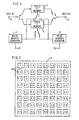
- Figure 1 shows in simplified block form a special effects equipment for a high definition video system;
- Figure 2 shows diagrammatically the arrangement of an embodiment of video signal memory according to the present invention and used in the equipment of Figure 1;
- Figure 3 shows diagrammatically the relationship between the video signal memory of Figure 2 and the raster of a cathode ray tube screen; and
- Figures 4 and 5 indicate diagrammatically examples of the use of the video signal memory of Figure 2.
- Before describing the embodiment, the overall arrangement of an example of a special effects equipment for the high definition video system outlined above will be briefly described with reference to Figure 1. Basically, the special effects equipment comprises two field memories, a field zero
memory 1 and a field onememory 2, together with awrite address generator 3 and aread address generator 4. These elements are interconnected byswitches input terminal 9 are selectively supplied by way of theswitch 5 to the field zeromemory 1 or the field onememory 2. Output data for supply to anoutput terminal 10 are selectively derived by theswitch 6 from the field zeromemory 1 or the field onememory 2. Thewrite address generator 3 and theread address generator 4 are selectively and alternately connected to the field zeromemory 1 and the field onememory 2 by theswitches - In operation of this special effects equipment, an input analog signal is sampled 2048 times per horizontal scan line and the resulting sample values are pulse code modulation coded into 8-bit words to form the input digital data which are supplied to the
input terminal 9. Writing proceeds alternately in the field zeromemory 1 and the field onememory 2 in dependence on the position of theswitch 5 and under the control of thewrite address generator 3. The necessary complex address calculations which are required so as not only to achieve simple writing and reading of the individual digital signals into and out of theappropriate memory write address generator 3 by way of aninput terminal 11 or under control of a signal supplied to theread address generator 4 by way of aninput terminal 12. The way in which this is done is not of significance to the present invention and will not therefore be described in further detail here. When a complete field has been written in thememory switches 5 to 8 change position and the digital signals stored in thatmemory read address generator 4 and supplied to theoutput terminal 10, while the digital signals for the next field are written in theother memory - The present invention is particularly concerned with the form and operation of the
memories - Referring to Figure 2, each of the
memories array 21 of n x n, where n is at least two and in this particular example n is equal to eight,memory modules 22. Eachmemory module 22 is addressed by its row and column number in thememory array 21 as indicated in Figure 2, although it will be understood that the actual physical positions of thememory modules 22 on a circuit board need not correspond to the indicated positions in thememory array 21. Eachmemory module 22 comprises a random access memory (RAM) and an associated latch circuit. Each of the RAMs can store m 8-bit words, where in this particular example m is equal to 16K, so thememory array 21 as a whole can store n2m words, which is sufficient for one field of the video signal. - Another way of considering the
memory array 21 is to say that it has eight rows and eight columns, and in the depth direction has 16K levels. Thus to write a word into thememory array 21 or to read it therefrom, the necessary address comprises level, row and column information. - Referring now to Figure 3, this relates the
memory array 21 of Figure 2 to thescreen 31 of a cathode ray tube. Each square in Figure 3 corresponds to one level of thememory array 21, and the numbers within each square correspond to the row and column numbers of therespective memory module 22 of Figure 2. Thus considering thescreen 31 in Figure 3, the first eight sample values in the first eight scan lines are stored in the top level or level zero of thememory array 21 of Figure 2, the next eight sample values in the first eight scan lines are stored in the level one of thememory array 21, and so on for the whole area of thescreen 31. - In use of the
memory array 21, up to eight 8-bit words corresponding to the respective sample values at up to eight adjacent collinear sample positions of the raster on thescreen 31 are written simultaneously. The effect of this is that no one of thememory modules 22 has more than one word written into it in each write cycle, even if the adjacent collinear sample positions overlap one or even two boundaries of the squares in Figure 3. This will be further described below with reference to Figures 4 and 5, but first the reason why up to eight sample values are written in each write cycle, rather than always eight, will be briefly explained. In fact, from the original digital data, the number of sample values selected for writing is always eight, but this number may decrease due to the special effects processing. To take a simple example, if the special effects processing involves halving the linear dimensions of an image, any eight adjacent collinear sample values initially selected will be reduced to four by the special effects processing. - Referring now to Figures 4 and 5, each of these shows the top right-hand square of Figure 3 and parts of the three immediately adjacent squares. These squares, corresponding to levels in the
memory modules 22, have level addresses which start at zero and progress sequentially along the top of thescreen 31, continue in the next row of squares and so on. It is assumed that the level address of the first square in the second row of squares is N. - Consider now the example of Figure 4. This shows the writing of eight adjacent collinear sample values disposed at zero degrees to the horizontal of the
screen 31. To write these eight sample values, eightmemory modules 22 in thememory array 21 are simultaneously addressed and are supplied with the respective 8-bit words representing the sample values to be stored therein.-The eight addresses are 0, 2, 3; 0, 2, 4; 0, 2, 5; 0, 2, 6; 0,2,7; 0,2,8; 1, 2, 1 and 1,2,2, where the first number designates the level in therespective memory module 22, the second number designates the row in thememory array 21 and the third number designates the column in thememory array 21. - Consider now the example of Figure 5. This shows the writing of eight adjacent collinear sample values disposed at 45 degrees to the horizontal of the
screen 31. To write these eight sample values, eightmemory modules 22 in thememory array 21 are simultaneously addressed and are supplied with the respective 8-bit words representing the sample values to be stored therein. The eight addresses are: 0,3,2; 0, 4, 3; 0, 5, 4; 0, 6, 5; 0, 7, 6; 0, 8, 7; N, 1, 8 and N + 1, 2,1, using the same notation as above. - From these examples it will be seen that by configuring the video memories and by having the write address generator (and calculator) 3 of Figure 1 present the addresses in this way, then even if the eight adjacent collinear sample values cross one or two boundaries between the squares on the
screen 31 of Figure 3, it is never necessary to write two words into thesame memory module 22 in the same write cycle. - The sample values referred to above are assumed to be the luminance sample values, and further, similar video signal memories operating the same way can be provided for the chrominance sample values.
- Various modifications are of course possible, and in particular the invention can be applied to video signal memories for use in other forms of television equipment and to frame memories. Also, the numbers n and m may be changed in consideration of the writing speed required and the amount of video digital data to be stored. Nor need the display be a cathode ray tube screen, as the invention can be used with other forms of raster display.
Claims (5)
characterized by: each said memory module (22) being arranged to store one only of said video data words in any square of n by n said sample positions of said raster in any one write cycle; and
Priority Applications (1)
| Application Number | Priority Date | Filing Date | Title |
|---|---|---|---|
| AT85306503T ATE53158T1 (en) | 1984-09-25 | 1985-09-12 | VIDEO SIGNAL MEMORY. |
Applications Claiming Priority (2)
| Application Number | Priority Date | Filing Date | Title |
|---|---|---|---|
| GB8424201 | 1984-09-25 | ||
| GB08424201A GB2164767B (en) | 1984-09-25 | 1984-09-25 | Video data storage |
Publications (2)
| Publication Number | Publication Date |
|---|---|
| EP0176289A1 EP0176289A1 (en) | 1986-04-02 |
| EP0176289B1 true EP0176289B1 (en) | 1990-05-23 |
Family
ID=10567224
Family Applications (1)
| Application Number | Title | Priority Date | Filing Date |
|---|---|---|---|
| EP85306503A Expired - Lifetime EP0176289B1 (en) | 1984-09-25 | 1985-09-12 | Video signal memories |
Country Status (6)
| Country | Link |
|---|---|
| US (1) | US4766496A (en) |
| EP (1) | EP0176289B1 (en) |
| AT (1) | ATE53158T1 (en) |
| CA (1) | CA1249378A (en) |
| DE (1) | DE3577959D1 (en) |
| GB (1) | GB2164767B (en) |
Families Citing this family (5)
| Publication number | Priority date | Publication date | Assignee | Title |
|---|---|---|---|---|
| GB8622611D0 (en) * | 1986-09-19 | 1986-10-22 | Questech Ltd | Processing of video image signals |
| US5208875A (en) * | 1989-03-07 | 1993-05-04 | Sony Corporation | Digital picture signal processing apparatus |
| GB2229059B (en) * | 1989-03-07 | 1993-08-04 | Sony Corp | Obtaining access to a two-dimensional portion of a digital picture signal |
| KR0122741B1 (en) * | 1992-09-23 | 1997-11-17 | 배순훈 | Memory having parallel architecture |
| GB2277012B (en) * | 1993-04-08 | 1997-06-18 | Sony Uk Ltd | Image data storage |
Family Cites Families (16)
| Publication number | Priority date | Publication date | Assignee | Title |
|---|---|---|---|---|
| FR1543788A (en) * | 1966-12-28 | Ibm | Multi-word multidirectional random access memory system | |
| US3643236A (en) * | 1969-12-19 | 1972-02-15 | Ibm | Storage having a plurality of simultaneously accessible locations |
| US3800289A (en) * | 1972-05-15 | 1974-03-26 | Goodyear Aerospace Corp | Multi-dimensional access solid state memory |
| US3996559A (en) * | 1974-11-07 | 1976-12-07 | International Business Machines Corporation | Method and apparatus for accessing horizontal sequences, vertical sequences and regularly spaced rectangular subarrays from an array stored in a modified word organized random access memory system |
| US4090174A (en) * | 1976-11-01 | 1978-05-16 | International Business Machines Corporation | Method and apparatus for accessing horizontal sequences, vertical sequences and rectangular subarrays from an array stored in a modified word organized random access memory system |
| DE2817556C2 (en) * | 1978-04-21 | 1982-09-09 | Robert Bosch Gmbh, 7000 Stuttgart | Method for controlling a dynamic memory |
| FR2480545A1 (en) * | 1980-04-10 | 1981-10-16 | Micro Consultants Ltd | DEVICE AND METHOD FOR PRINTING ANGULAR DISPLACEMENT TO A TELEVISION IMAGE |
| US4449199A (en) * | 1980-11-12 | 1984-05-15 | Diasonics Cardio/Imaging, Inc. | Ultrasound scan conversion and memory system |
| US4460958A (en) * | 1981-01-26 | 1984-07-17 | Rca Corporation | Window-scanned memory |
| US4432055A (en) * | 1981-09-29 | 1984-02-14 | Honeywell Information Systems Inc. | Sequential word aligned addressing apparatus |
| DE3141882A1 (en) * | 1981-10-22 | 1983-05-05 | Agfa-Gevaert Ag, 5090 Leverkusen | DYNAMIC WRITING AND READING MEMORY DEVICE |
| JPS58128078A (en) * | 1982-01-27 | 1983-07-30 | Dainippon Screen Mfg Co Ltd | Constituting method for memory device |
| GB2123998B (en) * | 1982-07-21 | 1986-10-22 | Marconi Avionics | Data memory arrangment |
| DE3374462D1 (en) * | 1982-07-21 | 1987-12-17 | Marconi Avionics | Multi-dimensional-access memory system |
| US4667190A (en) * | 1982-07-30 | 1987-05-19 | Honeywell Inc. | Two axis fast access memory |
| IT1156086B (en) * | 1982-10-25 | 1987-01-28 | Cselt Centro Studi Lab Telecom | METHOD AND STORAGE DEVICE OF NUMERICAL SIGNALS ORGANIZED IN A THREE-DIMENSIONAL WAY AND SUBJECT TO ORTHOGONAL TRANSFORMATIONS |
-
1984
- 1984-09-25 GB GB08424201A patent/GB2164767B/en not_active Expired
-
1985
- 1985-08-19 CA CA000488982A patent/CA1249378A/en not_active Expired
- 1985-09-12 AT AT85306503T patent/ATE53158T1/en not_active IP Right Cessation
- 1985-09-12 EP EP85306503A patent/EP0176289B1/en not_active Expired - Lifetime
- 1985-09-12 DE DE8585306503T patent/DE3577959D1/en not_active Expired - Lifetime
- 1985-09-17 US US06/776,958 patent/US4766496A/en not_active Expired - Lifetime
Also Published As
| Publication number | Publication date |
|---|---|
| GB8424201D0 (en) | 1984-10-31 |
| GB2164767A (en) | 1986-03-26 |
| GB2164767B (en) | 1988-08-24 |
| EP0176289A1 (en) | 1986-04-02 |
| DE3577959D1 (en) | 1990-06-28 |
| ATE53158T1 (en) | 1990-06-15 |
| US4766496A (en) | 1988-08-23 |
| CA1249378A (en) | 1989-01-24 |
Similar Documents
| Publication | Publication Date | Title |
|---|---|---|
| EP0176290B1 (en) | Video signal memories | |
| KR970000604B1 (en) | Multiple Serial Access Memory for Feedback System such as Motion Compensation Television, Digital Television Device Using the Same, and Method for Storing Video Data thereof | |
| CA1122696A (en) | Image rotation apparatus | |
| EP0264726B1 (en) | Picture transformation memory | |
| US4070662A (en) | Digital raster display generator for moving displays | |
| EP0895216B1 (en) | Image storage device and access method | |
| US4745479A (en) | Multiple image video display system | |
| US5027287A (en) | Device for the digital processing of images to obtain special geometrical effects | |
| US4581721A (en) | Memory apparatus with random and sequential addressing | |
| US4369504A (en) | Serial-parallel signal converter | |
| US4232376A (en) | Raster display refresh system | |
| US4063232A (en) | System for improving the resolution of alpha-numeric characters displayed on a cathode ray tube | |
| CA1141021A (en) | Processor for a graphic terminal | |
| GB1263281A (en) | Improvements relating to character display arrangements | |
| US4631531A (en) | System for text display with plural page memory and flag memory | |
| US5311211A (en) | Apparatus and method for providing a raster-scanned display with converted address signals for VRAM | |
| US4754279A (en) | Scan converter for radar | |
| US4766496A (en) | Video signal memories | |
| US6442297B1 (en) | Storage apparatus and writing and/or reading methods for use in hierarchical coding | |
| US4387395A (en) | Facsimile to video converter | |
| EP0180385A1 (en) | Video signal processing cicuits | |
| US5363140A (en) | Video signal conversion system with a vertical enhancement circuit | |
| US5289279A (en) | Video signal data recoding method for standard memory components and apparatus for perfomring the method | |
| US5818432A (en) | Character generator and video display device using the same | |
| JPH0830949B2 (en) | Video signal memory device |
Legal Events
| Date | Code | Title | Description |
|---|---|---|---|
| PUAI | Public reference made under article 153(3) epc to a published international application that has entered the european phase |
Free format text: ORIGINAL CODE: 0009012 |
|
| AK | Designated contracting states |
Kind code of ref document: A1 Designated state(s): AT DE FR GB NL |
|
| 17P | Request for examination filed |
Effective date: 19860820 |
|
| 17Q | First examination report despatched |
Effective date: 19890310 |
|
| GRAA | (expected) grant |
Free format text: ORIGINAL CODE: 0009210 |
|
| AK | Designated contracting states |
Kind code of ref document: B1 Designated state(s): AT DE FR GB NL |
|
| REF | Corresponds to: |
Ref document number: 53158 Country of ref document: AT Date of ref document: 19900615 Kind code of ref document: T |
|
| REF | Corresponds to: |
Ref document number: 3577959 Country of ref document: DE Date of ref document: 19900628 |
|
| ET | Fr: translation filed | ||
| PLBE | No opposition filed within time limit |
Free format text: ORIGINAL CODE: 0009261 |
|
| STAA | Information on the status of an ep patent application or granted ep patent |
Free format text: STATUS: NO OPPOSITION FILED WITHIN TIME LIMIT |
|
| 26N | No opposition filed | ||
| REG | Reference to a national code |
Ref country code: GB Ref legal event code: IF02 |
|
| PGFP | Annual fee paid to national office [announced via postgrant information from national office to epo] |
Ref country code: NL Payment date: 20040905 Year of fee payment: 20 |
|
| PGFP | Annual fee paid to national office [announced via postgrant information from national office to epo] |
Ref country code: GB Payment date: 20040908 Year of fee payment: 20 Ref country code: FR Payment date: 20040908 Year of fee payment: 20 |
|
| PGFP | Annual fee paid to national office [announced via postgrant information from national office to epo] |
Ref country code: DE Payment date: 20040909 Year of fee payment: 20 |
|
| PGFP | Annual fee paid to national office [announced via postgrant information from national office to epo] |
Ref country code: AT Payment date: 20040913 Year of fee payment: 20 |
|
| PG25 | Lapsed in a contracting state [announced via postgrant information from national office to epo] |
Ref country code: GB Free format text: LAPSE BECAUSE OF EXPIRATION OF PROTECTION Effective date: 20050911 |
|
| PG25 | Lapsed in a contracting state [announced via postgrant information from national office to epo] |
Ref country code: NL Free format text: LAPSE BECAUSE OF EXPIRATION OF PROTECTION Effective date: 20050912 |
|
| REG | Reference to a national code |
Ref country code: GB Ref legal event code: PE20 |
|
| NLV7 | Nl: ceased due to reaching the maximum lifetime of a patent |
Effective date: 20050912 |