EP0174729B2 - Optical amplification - Google Patents
Optical amplification Download PDFInfo
- Publication number
- EP0174729B2 EP0174729B2 EP85305572A EP85305572A EP0174729B2 EP 0174729 B2 EP0174729 B2 EP 0174729B2 EP 85305572 A EP85305572 A EP 85305572A EP 85305572 A EP85305572 A EP 85305572A EP 0174729 B2 EP0174729 B2 EP 0174729B2
- Authority
- EP
- European Patent Office
- Prior art keywords
- amplified
- signal
- wavelength
- driving current
- semiconductor laser
- Prior art date
- Legal status (The legal status is an assumption and is not a legal conclusion. Google has not performed a legal analysis and makes no representation as to the accuracy of the status listed.)
- Expired - Lifetime
Links
Images


Classifications
-
- H—ELECTRICITY
- H01—ELECTRIC ELEMENTS
- H01S—DEVICES USING THE PROCESS OF LIGHT AMPLIFICATION BY STIMULATED EMISSION OF RADIATION [LASER] TO AMPLIFY OR GENERATE LIGHT; DEVICES USING STIMULATED EMISSION OF ELECTROMAGNETIC RADIATION IN WAVE RANGES OTHER THAN OPTICAL
- H01S5/00—Semiconductor lasers
- H01S5/50—Amplifier structures not provided for in groups H01S5/02 - H01S5/30
-
- H—ELECTRICITY
- H01—ELECTRIC ELEMENTS
- H01S—DEVICES USING THE PROCESS OF LIGHT AMPLIFICATION BY STIMULATED EMISSION OF RADIATION [LASER] TO AMPLIFY OR GENERATE LIGHT; DEVICES USING STIMULATED EMISSION OF ELECTROMAGNETIC RADIATION IN WAVE RANGES OTHER THAN OPTICAL
- H01S5/00—Semiconductor lasers
- H01S5/06—Arrangements for controlling the laser output parameters, e.g. by operating on the active medium
- H01S5/068—Stabilisation of laser output parameters
- H01S5/0683—Stabilisation of laser output parameters by monitoring the optical output parameters
-
- H—ELECTRICITY
- H01—ELECTRIC ELEMENTS
- H01S—DEVICES USING THE PROCESS OF LIGHT AMPLIFICATION BY STIMULATED EMISSION OF RADIATION [LASER] TO AMPLIFY OR GENERATE LIGHT; DEVICES USING STIMULATED EMISSION OF ELECTROMAGNETIC RADIATION IN WAVE RANGES OTHER THAN OPTICAL
- H01S5/00—Semiconductor lasers
- H01S5/06—Arrangements for controlling the laser output parameters, e.g. by operating on the active medium
- H01S5/068—Stabilisation of laser output parameters
- H01S5/0683—Stabilisation of laser output parameters by monitoring the optical output parameters
- H01S5/0687—Stabilising the frequency of the laser
-
- H—ELECTRICITY
- H01—ELECTRIC ELEMENTS
- H01S—DEVICES USING THE PROCESS OF LIGHT AMPLIFICATION BY STIMULATED EMISSION OF RADIATION [LASER] TO AMPLIFY OR GENERATE LIGHT; DEVICES USING STIMULATED EMISSION OF ELECTROMAGNETIC RADIATION IN WAVE RANGES OTHER THAN OPTICAL
- H01S5/00—Semiconductor lasers
- H01S5/50—Amplifier structures not provided for in groups H01S5/02 - H01S5/30
- H01S5/5063—Amplifier structures not provided for in groups H01S5/02 - H01S5/30 operating above threshold
-
- H—ELECTRICITY
- H01—ELECTRIC ELEMENTS
- H01S—DEVICES USING THE PROCESS OF LIGHT AMPLIFICATION BY STIMULATED EMISSION OF RADIATION [LASER] TO AMPLIFY OR GENERATE LIGHT; DEVICES USING STIMULATED EMISSION OF ELECTROMAGNETIC RADIATION IN WAVE RANGES OTHER THAN OPTICAL
- H01S5/00—Semiconductor lasers
- H01S5/50—Amplifier structures not provided for in groups H01S5/02 - H01S5/30
- H01S5/5081—Amplifier structures not provided for in groups H01S5/02 - H01S5/30 specifically standing wave amplifiers
Definitions
- the present invention relates to the amplification of optical signals.
- optical signals The amplification of optical signals is of especial importance in optical communications.
- the radiation used in optical communications is not necessarily in the visible region, and the words "optical” and 'light" when used in this specification are not to be interpreted as implying any such limitations. Indeed, of silica optical fibres are used as the transmission medium, infra-red radiation is of especial usefulness because the loss mirima occur in such fibres at 1.3 ⁇ m and 1.55 ⁇ m approximately.
- a semiconductor laser comprises in general an "active layer" of low band gap material with higher band gap “confinement” layers to either side and a p-n junction in the vicinity of the active layer.
- active layer When current is passed from p- to n-type material, electrons and holes combine in the active layer to generate light
- the threshold current at which the onset of "lasing" occurs depends on the degree of feedback into the structure, e.g. by reflections from its end faces, on the (current dependent) gain through stimulated emission as photons pass along the active layer, and on other factors.
- the laser functions as a light emitting diode or as a superluminescent emitter.
- a laser in which the feedback is provided by reflections at end facets is known as a Fabry-Perot laser.
- a semiconductor laser structure can be used as an optical amplifier cf. e.g. EP-A-0 060 033.
- a laser structure is chosen having a wavelength of maximum gain close to the wavelength of the optical signal to be amplified and this signal is coupled into its active layer then it can be amplified if a driving current of less than the threshold value is passed through the structure from p- to n-type material.
- the phrase "laser structure" is used here and elsewhere in this specification to indicate the similarity of the amplifier structure to that of a laser without necessarily implying that lasing actually occurs in use.
- the amplifier gain for a given driving current is substantially constant from zero input power over a range of lower powers and then decreases to zero and then becomes negative (i.e. net absorption occurs) with higher powers. This is at least partly because the device saturates as the proportion of the available holes and electrons consumed increases. Increasing the driving current can be used to increase the supply of holes and electrons and therefore the gain; however, the extent to which this can be done is limited, because around the lasing threshold of the device injection-locked lasing occurs whereafterthe dependence or the power input of the power output at the single emission wavelength is slight, i.e. useful amplification does not occur.
- An object of the present invention is to provide means for amplifying higher input powers.
- the present invention in its first aspect is based on our surprising discovery that the effects of saturation are less marked on the long-wavelength side of the wavelength of maximum gain as measured for lower powers.
- the present invention provides a method of amplifying an optical signal which comprises coupling the optical signal to be amplified into the active layer of a semiconductor laser hetero-structure through which a driving current is passed, the amplified signal being emitted from the active layer, in which method the wavelength of the gain maximum at that driving current for the low power limit of optical power input ⁇ max , the longer of the two wavelengths of zero gain at the driving current for the low power limit of optical power input ⁇ upper , and the wavelength of the optical signal to be amplified A are related by the relationships ⁇ upper > ⁇ > ⁇ max , and ( ⁇ - ⁇ max ) / ( ⁇ upper - ⁇ max ) ⁇ 0.1.
- the present invention further provides an amplification assembly for amplifying an optical signal which comprises an optical signal source, a semiconductor laser hetero-structure, means for coupling the optical signal to be amplified into the active layer of the semiconductor laser hetero-structure, and means for passing a driving current through the semiconductor laser hetero-structure, the amplified signal being emitted from the active layer in use, wherein the wavelength of the gain maximum of the semiconductor laser hetero-structure at that driving current for the low power limit of optical power input ⁇ max , the longer of the two wavelength of zero gain at the driving current ⁇ upper , and the wavelength of the optical signal to be amplified A are related by relationships ⁇ upper > ⁇ > ⁇ max , and ( ⁇ - ⁇ max ) / ( ⁇ upper - ⁇ max ) ⁇ 0.1.
- ( ⁇ - ⁇ max ) / ( ⁇ upper - ⁇ max ) is at least 0.2.
- our invention is based on our appreciation that if the input wavelength is sufficiently remote from the wavelength of the laser gain maximum to avoid injection-locking, whether on the high side or the low side, useful amplification of the input signal can be obtained with currents in excess of the threshold current.
- the present invention provides a method of amplifying an optical signal which comprises coupling the signal to be amplified into the active layer of a semiconductor laser structure and applying a driving current to the laser structure such that lasing occurs, the wavelength of the signal to be amplified being such that injection locking is avoided and the amplified signal is emitted from the active layer.
- the present invention further provides an amplification assembly for amplifying an optical signal which comprises an optical signal source, a semiconductor laser structure, means for coupling the optical signal to be amplified into the active layer of the semiconductor laser structure, and means for passing a driving current through the semiconductor laser structure such that lasing occurs, the wavelength of the signal to be amplified being such that injection locking is avoided and the amplified signal being emitted from the active layer.
- an amplification assembly for amplifying an optical signal which comprises an optical signal source, a semiconductor laser structure, means for coupling the optical signal to be amplified into the active layer of the semiconductor laser structure, and means for passing a driving current through the semiconductor laser structure such that lasing occurs, the wavelength of the signal to be amplified being such that injection locking is avoided and the amplified signal being emitted from the active layer.
- the present invention is based on our appreciation that the output of a laser structure under use as an optical amplifier is diminished over its entire emission range (not merely at the wavelength of the input signal) by the saturation referred to above and that this diminution offers a means of controlling the current so as to raise up the amplifier gain at higher input powers.
- the present invention provides a method of amplifying an optical signal which comprises coupling the signal to be amplified into the active layer of a semiconductor laser structure through which a driving current is passed, which layer emits the amplified signal, and monitoring the light emission from the active layer at a wavelength or over a wavelength range distinct from that of the amplified signal, and controlling the driving current to the laser structure so as at least partly to compensate for the decrease in the monitored output with increasing optical input.
- the present invention further provides an amplification assembly for amplifying an optical signal which comprises an optical signal source, a semiconductor laser structure, means for coupling the optical signal to be amplified into the active layer of the semiconductor laser structure, and means for passing a driving current through the semiconductor laser structure, the amplified signal being emitted from the active layer in use, wherein means is provided to monitor the output of the semiconductor laser structure at a wavelength or over a wavelength range distinct from that of the amplified signal, and a feedback control loop is provided which acts to control the driving current so as at least partly to compensate for the decrease in the monitored output with increased optical input power.
- the invention can be employed independently in each of its three aspects, or in all three simultaneously, or in any of the three possible combinations of two aspects.
- the invention can even be applied to a laser structure with so little feedback that it cannot be made to lase at any practical current (e.g. a travelling wave amplifier).
- Figure 1 shows how in a typical semiconductor laser amplifier the signal intensity S varies with length along the cavity of the amplifier.
- the signal intensity S comprises two components 21, 22 representing the forward and reflected waves travelling in opposed directions along the amplifier.
- the variation in signal intensity S along the length 1 of the amplifier leads to consequent variation in carrier density and gain.
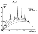
- Figure 2 shows results for the gain characteristics obtained by use of this model for a Fabry-Perot laser amplifier operable near the 1.55 ⁇ m loss minimum of silica fibres in which the reflectivity of each end facet is taken to be 0.01.
- the current density is taken to be 0.97 times the threshold current density.
- the mode spacing of the laser is taken as 1 nm.
- the detailed results of calculations for various input powers are shown only for selected wavelengths so as to avoid congestion.
- the dotted lines which connect the results shown represent the general trend of the gain characteristics between these results without including detail.
- the gain characteristics show Fabry-Perot resonances.
- the trend in the characteristics follows the trend of the material gain spectrum with the largest values of the amplification occurring at the gain peak at 1.5525 ⁇ m.
- the carrier density decreases. This reduces the amplification overall and shifts the gain peak to longer wavelengths as well as modifying the carrier-dependent refractive index.
- the gain peak has already shifted to a longer wavelength; 1.5572 ⁇ m.
- the reduction in gain (13.7 dB to 13.0 dB) seen at the wavelength of maximum gain at low power 1.5525 ⁇ m, when the input power is increased to 10 ⁇ 6W, can therefore be at least partially offset by operation at up to at least 1.5572 ⁇ m.
- the further benefit referred to above is that of reduced sensitivity to increases over a range of input power. It can be seen that the reduction in gain at 1.5525 ⁇ m over the range of input powers shown is just over 37% whereas the reduction in gain at 1.5700 ⁇ m is slightly less than 27%. This reduced sensitivity to increases in input power gives the amplifier the desirable feature of having a more linear gain characteristic for increasing signal input powers. In contrast, the equivalent reduction in gain at 1.5400 ⁇ m is more than 47%.
- 1 represents an optical fibre carrying an input signal of wavelength 1580 nm (1.58 ⁇ m) from an optical signal source (not shown). This is coupled from the fibre end into activer layer 3 of a Fabry-Perot laser structure 2.
- This structure is one having a maximum gain at the low power limit of optical power input at a wavelength of 1550 nm (1.55 ⁇ m), the positive part of the gain spectrum at the low power limit of optical power input extending to 1600 nm (1.60 ⁇ m) on the long wavelength side and having an approximately similar extent to the low wavelength side.
- Current of above the threshold level is passed between electrodes 4 and 5 and lasing occurs in various Fabry-Perot modes distributed over the gain spectrum.
- Amplification occurs at the wavelength 1580 nm of the input signal.
- Light emerges from 3 and is fed via lens 6 into interference filter 7.
- the interference filter reflects a band of radiation near to 1550 nm but not significantly the radiation at 1580 nm to lens 8 and optical detector 9.
- the signal including the amplified 1580 nm signal continues to lens 10 and the output optical fibre 11.
- the gain for high input powers from fibre 1 is higher than would have been the case had the wavelength of maximum gain of laser 2 been at 1.58 ⁇ m for the low power limit.
- the difference between ⁇ and ⁇ max is such that amplification occurs even for currents of above threshold, and this higher permitted current makes also for high gain. (This latter effect would be present even had the input radiation been at (say) 1.52 ⁇ m, i.e. had the first aspect of the invention not been exploited).
- a further although independent benefit is afforded, in accordance with the present invention in its third aspect, by the use of a feedback control loop.
- the loop comprises the filter 7, the lens 8, the detector 9 and the control circuit 12 which receives the output signal of the detector 9.
- the control circuit 12 is designed to adjust the current passed between electrodes 4 and 5 to maintain a constant output from detector 9, and thereby constant amplifier gain. This circuitry would, it should be mentioned, be of value even in operation with currents below lasing threshold.
- the end facets will normally be anti-reflection coated, e.g. to achieve reflectivities of 0.01.
- One use of the device shown, and indeed generally of methods and amplification assemblies in accordance with the present invention, is in optical communications systems where the light from the laser source is passed through lossy components such as modulators or optical isolators before being coupled into the optical fibre of the communications link. Such arrangements are of especial significance for coherent optical systems.
- the signal emerging from these lossy components can be amplified to make up for the losses.
- the input powers desired in such cases are in general high ones in the context of this specification, and therefore ones where the present invention affords advantages. Gains of about 10 dB are achievable even for input powers of 5 mW. Power on launch into the communications link is of course of the greatest importance in determining repeater spacings.
- the source laser and the amplifying laser devices that are practically identical except that the latter is anti-reflection coated.
- the source laser will lase at relatively low currents with a wavelength longer than that of the amplifier laser when made to lase with the relatively high currents that are necessary, and longer than the wavelength of maximum gain at low powers of the amplifier laser. In this way one can with relative ease secure the benefits in accordance with the present invention in its first aspect.
- the methods and amplification assemblies in accordance with the present invention may also be used in optical preamplifiers, for instance before a detector at the receiving end of an optical signalling arrangement.
Landscapes
- Physics & Mathematics (AREA)
- Condensed Matter Physics & Semiconductors (AREA)
- General Physics & Mathematics (AREA)
- Electromagnetism (AREA)
- Optics & Photonics (AREA)
- Semiconductor Lasers (AREA)
- Optical Communication System (AREA)
Description
- The present invention relates to the amplification of optical signals.
- The amplification of optical signals is of especial importance in optical communications. The radiation used in optical communications is not necessarily in the visible region, and the words "optical" and 'light" when used in this specification are not to be interpreted as implying any such limitations. Indeed, of silica optical fibres are used as the transmission medium, infra-red radiation is of especial usefulness because the loss mirima occur in such fibres at 1.3 µm and 1.55 µm approximately.
- A semiconductor laser comprises in general an "active layer" of low band gap material with higher band gap "confinement" layers to either side and a p-n junction in the vicinity of the active layer. When current is passed from p- to n-type material, electrons and holes combine in the active layer to generate light The threshold current at which the onset of "lasing" occurs depends on the degree of feedback into the structure, e.g. by reflections from its end faces, on the (current dependent) gain through stimulated emission as photons pass along the active layer, and on other factors. At lower currents, the laser functions as a light emitting diode or as a superluminescent emitter. A laser in which the feedback is provided by reflections at end facets is known as a Fabry-Perot laser.
- It is known that a semiconductor laser structure can be used as an optical amplifier cf. e.g. EP-A-0 060 033. Thus, it is known that if a laser structure is chosen having a wavelength of maximum gain close to the wavelength of the optical signal to be amplified and this signal is coupled into its active layer then it can be amplified if a driving current of less than the threshold value is passed through the structure from p- to n-type material. The phrase "laser structure" is used here and elsewhere in this specification to indicate the similarity of the amplifier structure to that of a laser without necessarily implying that lasing actually occurs in use.
- We have given attention to the characteristic of such amplifiers that the amplifier gain for a given driving current is substantially constant from zero input power over a range of lower powers and then decreases to zero and then becomes negative (i.e. net absorption occurs) with higher powers. This is at least partly because the device saturates as the proportion of the available holes and electrons consumed increases. Increasing the driving current can be used to increase the supply of holes and electrons and therefore the gain; however, the extent to which this can be done is limited, because around the lasing threshold of the device injection-locked lasing occurs whereafterthe dependence or the power input of the power output at the single emission wavelength is slight, i.e. useful amplification does not occur.
- An object of the present invention is to provide means for amplifying higher input powers.
- The present invention in its first aspect is based on our surprising discovery that the effects of saturation are less marked on the long-wavelength side of the wavelength of maximum gain as measured for lower powers.
- In its first aspect the present invention provides a method of amplifying an optical signal which comprises coupling the optical signal to be amplified into the active layer of a semiconductor laser hetero-structure through which a driving current is passed, the amplified signal being emitted from the active layer, in which method the wavelength of the gain maximum at that driving current for the low power limit of optical power input λmax, the longer of the two wavelengths of zero gain at the driving current for the low power limit of optical power input λupper, and the wavelength of the optical signal to be amplified A are related by the relationships

and
- In its first aspect the present invention further provides an amplification assembly for amplifying an optical signal which comprises an optical signal source, a semiconductor laser hetero-structure, means for coupling the optical signal to be amplified into the active layer of the semiconductor laser hetero-structure, and means for passing a driving current through the semiconductor laser hetero-structure, the amplified signal being emitted from the active layer in use, wherein the wavelength of the gain maximum of the semiconductor laser hetero-structure at that driving current for the low power limit of optical power input λmax, the longer of the two wavelength of zero gain at the driving current λupper, and the wavelength of the optical signal to be amplified A are related by relationships

and
- Preferably, (λ - λmax) / (λupper - λmax) is at least 0.2.
- In a second aspect, our invention is based on our appreciation that if the input wavelength is sufficiently remote from the wavelength of the laser gain maximum to avoid injection-locking, whether on the high side or the low side, useful amplification of the input signal can be obtained with currents in excess of the threshold current.
- In its second aspect, therefore, the present invention provides a method of amplifying an optical signal which comprises coupling the signal to be amplified into the active layer of a semiconductor laser structure and applying a driving current to the laser structure such that lasing occurs, the wavelength of the signal to be amplified being such that injection locking is avoided and the amplified signal is emitted from the active layer.
- In its second aspect, the present invention further provides an amplification assembly for amplifying an optical signal which comprises an optical signal source, a semiconductor laser structure, means for coupling the optical signal to be amplified into the active layer of the semiconductor laser structure, and means for passing a driving current through the semiconductor laser structure such that lasing occurs, the wavelength of the signal to be amplified being such that injection locking is avoided and the amplified signal being emitted from the active layer.
- In a third aspect, the present invention is based on our appreciation that the output of a laser structure under use as an optical amplifier is diminished over its entire emission range (not merely at the wavelength of the input signal) by the saturation referred to above and that this diminution offers a means of controlling the current so as to raise up the amplifier gain at higher input powers.
- In this third aspect, therefore, the present invention provides a method of amplifying an optical signal which comprises coupling the signal to be amplified into the active layer of a semiconductor laser structure through which a driving current is passed, which layer emits the amplified signal, and monitoring the light emission from the active layer at a wavelength or over a wavelength range distinct from that of the amplified signal, and controlling the driving current to the laser structure so as at least partly to compensate for the decrease in the monitored output with increasing optical input.
- In its third aspect, the present invention further provides an amplification assembly for amplifying an optical signal which comprises an optical signal source, a semiconductor laser structure, means for coupling the optical signal to be amplified into the active layer of the semiconductor laser structure, and means for passing a driving current through the semiconductor laser structure, the amplified signal being emitted from the active layer in use, wherein means is provided to monitor the output of the semiconductor laser structure at a wavelength or over a wavelength range distinct from that of the amplified signal, and a feedback control loop is provided which acts to control the driving current so as at least partly to compensate for the decrease in the monitored output with increased optical input power.
- The invention can be employed independently in each of its three aspects, or in all three simultaneously, or in any of the three possible combinations of two aspects. In its first and third aspects, the invention can even be applied to a laser structure with so little feedback that it cannot be made to lase at any practical current (e.g. a travelling wave amplifier).
- The invention will now be described by way of example only, with respect to the accompanying Figures 1 to 4 in which:-
- Figure 1 shows the photon distribution along the cavity of a semiconductor laser amplifier;
- Figure 2 shows the gain characteristics at different input powers of a particular semiconductor laser amplifier as calculated by means of a computer model (only selected results being shown);
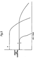
- Figure 3 shows (schematically, smoothed, and generalised) the results of calculations such as those selected for inclusion in Figure 2; and
- Figure 4 shows, schematically and not to scale, a semiconductor laser amplification assembly which is an embodiment of the present invention in all three aspects.
- Figure 1 shows how in a typical semiconductor laser amplifier the signal intensity S varies with length along the cavity of the amplifier. The signal intensity S comprises two
components - We have constructed an analytical model of the laser amplifier in which the total
axial photon distribution 23 is averaged over the cavity length and used to self-consistently determine a uniform carrier density. We have incorporated the refinement of a spectrally dependent gain function (the peak of which shifts with the carrier density) and the effect of carrier density on the refractive index within the cavity. - Figure 2 shows results for the gain characteristics obtained by use of this model for a Fabry-Perot laser amplifier operable near the 1.55 µm loss minimum of silica fibres in which the reflectivity of each end facet is taken to be 0.01. The current density is taken to be 0.97 times the threshold current density. The mode spacing of the laser is taken as 1 nm. The detailed results of calculations for various input powers are shown only for selected wavelengths so as to avoid congestion. The dotted lines which connect the results shown represent the general trend of the gain characteristics between these results without including detail.
- It will be seen that the gain characteristics, as well as depending on wavelength and input power, show Fabry-Perot resonances. At the lowest input power the trend in the characteristics follows the trend of the material gain spectrum with the largest values of the amplification occurring at the gain peak at 1.5525 µm. With increasing input power the carrier density decreases. This reduces the amplification overall and shifts the gain peak to longer wavelengths as well as modifying the carrier-dependent refractive index.
- It can be seen that the gain peak shifts according to the following Table:

- Hence when the input power is increased from 10⁻¹⁰W to 10⁻⁶W, the gain peak has already shifted to a longer wavelength; 1.5572 µm. The reduction in gain (13.7 dB to 13.0 dB) seen at the wavelength of maximum gain at low power 1.5525 µm, when the input power is increased to 10⁻⁶W, can therefore be at least partially offset by operation at up to at least 1.5572 µm.
- Referring still to Figure 2, as the input power is further increased, increasingly significant reductions in overall amplification are seen. At the same time the gain peak is shifted to increasingly longer wavelengths. The result is that increasing benefit is available, in offsetting the overall reduction in amplification by operating at longer wavelengths, as the input power is increased from 10⁻¹⁰W to 10⁻⁶W, 10⁻⁵W and through the values shown to 5×10⁻⁵W. It has further been observed, though not shown in Figure 2, that particularly significant benefit can be had at input powers of the order of 1 mW, for instance at input powers of 0.5 mW to 5 mW inclusive.
- In Figure 3 the amplifier gain as a function of input power for a given current is shown for three different wavelengths, B near to the wavelength of maximum gain, A somewhere on the low wavelength side but within the positive part of the gain curve, and C on the long-wavelength side but likewise within the positive part of the gain curve, C showing a gain at lower power similar to that of curve A. The effect of Fabry-Perot resonances has been smoothed out. It will be seen from the part of the Figure where curve C lies highest why, if one wishes to amplify a higher input power at a particular wavelength, one can achieve best results (in accordance with the invention in its first aspect) by using a laser amplifier of which the maximum gain at low power is at a shorter wavelength than the signal to be amplified.
- Referring again to Figure 2, it can be seen that there is a further benefit to be gained from operating at an input wavelength which is greater than the wavelength of maximum gain at low powers. The variation in gain due to increasing input powers for the wavelength of maximum gain at low powers, and for two wavelengths selected to be longer and shorter respectively, are shown in the following Table:

- The further benefit referred to above is that of reduced sensitivity to increases over a range of input power. It can be seen that the reduction in gain at 1.5525 µm over the range of input powers shown is just over 37% whereas the reduction in gain at 1.5700 µm is slightly less than 27%. This reduced sensitivity to increases in input power gives the amplifier the desirable feature of having a more linear gain characteristic for increasing signal input powers. In contrast, the equivalent reduction in gain at 1.5400 µm is more than 47%.
- We refer now to Figure 4.
- In Figure 4, 1 represents an optical fibre carrying an input signal of wavelength 1580 nm (1.58 µm) from an optical signal source (not shown). This is coupled from the fibre end into activer layer 3 of a Fabry-
Perot laser structure 2. This structure is one having a maximum gain at the low power limit of optical power input at a wavelength of 1550 nm (1.55 µm), the positive part of the gain spectrum at the low power limit of optical power input extending to 1600 nm (1.60 µm) on the long wavelength side and having an approximately similar extent to the low wavelength side. Current of above the threshold level is passed betweenelectrodes 4 and 5 and lasing occurs in various Fabry-Perot modes distributed over the gain spectrum. - Amplification occurs at the wavelength 1580 nm of the input signal. Light emerges from 3 and is fed via lens 6 into interference filter 7. The interference filter reflects a band of radiation near to 1550 nm but not significantly the radiation at 1580 nm to lens 8 and optical detector 9. The signal including the amplified 1580 nm signal continues to
lens 10 and the output optical fibre 11. (λ-λmax)/(λupper-λmax) as defined above is 0.6. - In accordance with the invention in its first aspect, the gain for high input powers from fibre 1 is higher than would have been the case had the wavelength of maximum gain of
laser 2 been at 1.58 µm for the low power limit. In accordance with the invention in its second aspect, the difference between λ and λmax is such that amplification occurs even for currents of above threshold, and this higher permitted current makes also for high gain. (This latter effect would be present even had the input radiation been at (say) 1.52 µm, i.e. had the first aspect of the invention not been exploited). - In the Figure, a further although independent benefit is afforded, in accordance with the present invention in its third aspect, by the use of a feedback control loop. The loop comprises the filter 7, the lens 8, the detector 9 and the control circuit 12 which receives the output signal of the detector 9. The control circuit 12 is designed to adjust the current passed between
electrodes 4 and 5 to maintain a constant output from detector 9, and thereby constant amplifier gain. This circuitry would, it should be mentioned, be of value even in operation with currents below lasing threshold. - For optimum performance in the device described, the end facets will normally be anti-reflection coated, e.g. to achieve reflectivities of 0.01.
- Semiconductor laser structures other than that described above may be employed. However, their characteristics, such as the input power at which significant benefits may be gained by application of the present invention, will vary from those described above.
- One use of the device shown, and indeed generally of methods and amplification assemblies in accordance with the present invention, is in optical communications systems where the light from the laser source is passed through lossy components such as modulators or optical isolators before being coupled into the optical fibre of the communications link. Such arrangements are of especial significance for coherent optical systems. By using the device shown, the signal emerging from these lossy components can be amplified to make up for the losses. The input powers desired in such cases are in general high ones in the context of this specification, and therefore ones where the present invention affords advantages. Gains of about 10 dB are achievable even for input powers of 5 mW. Power on launch into the communications link is of course of the greatest importance in determining repeater spacings.
- In such an application it is possible to use as the source laser and the amplifying laser devices that are practically identical except that the latter is anti-reflection coated. The source laser will lase at relatively low currents with a wavelength longer than that of the amplifier laser when made to lase with the relatively high currents that are necessary, and longer than the wavelength of maximum gain at low powers of the amplifier laser. In this way one can with relative ease secure the benefits in accordance with the present invention in its first aspect.
- The methods and amplification assemblies in accordance with the present invention may also be used in optical preamplifiers, for instance before a detector at the receiving end of an optical signalling arrangement.
Claims (22)
- A method of amplifying an optical signal which comprises coupling the optical signal to be amplified into the active layer of a semiconductor laser hetero-structure through which a driving current is passed, the amplified signal being emitted from the active layer, in which method the wavelength of the gain maximum at that driving current for the low power limit of optical power input λmax, the longer of the two wavelengths of zero gain at the driving current for the low power limit of optical power input λupper, and the wavelength of the optical signal to be amplified λ are related by the relationships


- A method according to claim 1, wherein

- A method according to any preceding claim wherein λmax is in the range from 1.2 to 1. 7µm.
- A method according to any preceding claim wherein the driving current is such that lasing does not occur.
- A method according to any of claims 1 to 3, wherein the driving current is such that lasing occurs and the wavelength of the optical signal to be amplified is such that injection locking of the laser does not occur.
- A method of amplifying an optical signal which comprises coupling the signal to be amplified into the active layer of a semiconductor laser structure and applying a driving current to the laser structure such that lasing occurs, the wavelength of the signal to be amplified being such that injection locking is avoided and the amplified signal is emitted from the active layer.
- A method according to any one of claims 1 to 6 wherein the output of the semiconductor laser structure is monitored at a wavelength or over a wavelength range distinct from that of the amplified signal and the driving current is controlled so as at least partly to compensate for the decrease in the monitored output with increased optical input.
- A method of amplifying an optical signal which comprises coupling the signal to be amplified into the active layer of a semiconductor laser structure through which a driving current is passed, which layer emits the amplified signal, and monitoring the light emission from the active layer at a wavelength or over a wavelength range distinct from that of the amplified signal, and controlling the driving current to the laser structure so as at least partly to compensate for the decrease in the monitored output with increasing optical input.
- A method according to any preceding claim, wherein the signal to be amplified has a power which lies in the range from 1µW to 5mW inclusive.
- A method according to any preceding claim, wherein the signal to be amplified has a power which lies in the range from 10µW to 5mW inclusive.
- An amplification assembly for amplifying an optical signal which comprises an optical signal source, a semiconductor laser hetero-structure, means for coupling the optical signal to be amplified into the active layer of the semiconductor laser hetero-structure, and means for passing a driving current through the semiconductor laser hetero-structure, the amplified signal being emitted from the active layer in use, wherein the wavelength of the gain maximum of the semiconductor laser hetero-structure at that driving current for the low power limit of optical power input λmax, the longer of the two wavelengths of zero gain at the driving current for the low power limit of optical power input λupper, and the wavelength of the optical signal to the amplified λ are related by the relationships


- An assembly according to claim 11, wherein

- An assembly according to claim 11 or claim 12, wherein λmax is in the range from 1.2 to 1.7µm.
- An assembly according to any of claims 11 to 13, wherein the driving current is such that lasing does not occur.
- An assembly according to any of claims 11 to 13 wherein the driving current is such that lasing occurs and the wavelength of the optical signal to be amplified is such that injection locking of the laser does not occur.
- An amplification assembly for amplifying an optical signal which comprises an optical signal source, a semiconductor laser structure, means for coupling the optical signal to be amplified into the active layer of the semiconductor laser structure, and means for passing a driving current through the semiconductor laser structure such that lasing occurs, the wavelength of the signal to be amplified being such that injection locking is avoided and the amplified signal being emitted from the active layer.
- An assembly according to any one of claims 11 to 16 wherein means is provided to monitor the output of the semiconductor laser structure at a wavelength or over a wavelength range distinct from that of the amplified signal and a feedback control loop is provided which acts to control the driving current so as at least partly to compensate for the decrease in the monitored output with increased optical input power.
- An amplification assembly for amplifying an optical signal which comprises an optical signal source, a semiconductor laser structure, means for coupling the optical signal to be amplified into the active layer of the semiconductor laser structure, and means for passing a driving current through the semiconductor laser structure, the amplified signal being emitted from the active layer in use, wherein means is provided to monitor the output of the semiconductor laser structure at a wavelength or over a wavelength range distinct from that of the amplified signal and a feedback control loop is provided which acts to control the driving current so as at least partly to compensate for the decrease in the monitored output with increased optical input power.
- An assembly according to any one of claims 11 to 18, wherein the signal to be amplified has a power which lies in the range from 1µW to 5mW inclusive.
- An assembly according to any one of claims 11 to 18, wherein the signal to be amplified has a power which lies in the range from 10µW to 5mW.
- An assembly according to any one of claims 11 to 18, wherein the signal to be amplified has a power which lies in the range from 0.5mW to 5mW inclusive.
- An assembly according to any one of claims 11 to 21, wherein the semiconductor laser structure is of a Fabry-Perot type.
Priority Applications (1)
| Application Number | Priority Date | Filing Date | Title |
|---|---|---|---|
| AT85305572T ATE39396T1 (en) | 1984-08-06 | 1985-08-06 | OPTICAL AMPLIFICATION. |
Applications Claiming Priority (4)
| Application Number | Priority Date | Filing Date | Title |
|---|---|---|---|
| GB848420013A GB8420013D0 (en) | 1984-08-06 | 1984-08-06 | Optical amplification |
| GB8420013 | 1984-08-06 | ||
| GB848424860A GB8424860D0 (en) | 1984-10-02 | 1984-10-02 | Optical amplification |
| GB8424860 | 1984-10-02 |
Publications (3)
| Publication Number | Publication Date |
|---|---|
| EP0174729A1 EP0174729A1 (en) | 1986-03-19 |
| EP0174729B1 EP0174729B1 (en) | 1988-12-21 |
| EP0174729B2 true EP0174729B2 (en) | 1995-10-25 |
Family
ID=26288082
Family Applications (1)
| Application Number | Title | Priority Date | Filing Date |
|---|---|---|---|
| EP85305572A Expired - Lifetime EP0174729B2 (en) | 1984-08-06 | 1985-08-06 | Optical amplification |
Country Status (5)
| Country | Link |
|---|---|
| US (1) | US4736164A (en) |
| EP (1) | EP0174729B2 (en) |
| JP (1) | JPH0732276B2 (en) |
| CA (1) | CA1251845A (en) |
| DE (1) | DE3566937D1 (en) |
Families Citing this family (23)
| Publication number | Priority date | Publication date | Assignee | Title |
|---|---|---|---|---|
| US5017885A (en) * | 1984-05-10 | 1991-05-21 | At&T Bell Laboratories | Optical amplifier with reduced nonlinearity |
| US5089787A (en) * | 1985-05-05 | 1992-02-18 | California Institute Of Technology | Optically-coupled high frequency amplifier |
| GB8611241D0 (en) * | 1986-05-08 | 1986-06-18 | British Telecomm | Optical amplifiers |
| GB8709224D0 (en) * | 1987-04-16 | 1987-06-10 | British Telecomm | Optical amplifier |
| US4947134A (en) * | 1987-10-30 | 1990-08-07 | American Telephone And Telegraph Company | Lightwave systems using optical amplifiers |
| JPH01287426A (en) * | 1988-05-13 | 1989-11-20 | Hamamatsu Photonics Kk | Optical signal sampling device |
| JPH07109916B2 (en) * | 1988-05-26 | 1995-11-22 | 浜松ホトニクス株式会社 | Light intensity stabilizer |
| ES2044123T3 (en) * | 1988-07-20 | 1994-01-01 | American Telephone & Telegraph | OPTICAL AMPLIFIER WITH REDUCED ALIGNMENT. |
| GB2230912B (en) | 1989-04-22 | 1993-10-20 | Stc Plc | Optical amplifier gain control |
| JPH0357288A (en) * | 1989-07-17 | 1991-03-12 | Siemens Ag | Devices with semiconductor lasers and their usage |
| JPH04355986A (en) * | 1990-06-26 | 1992-12-09 | Canon Inc | Light source driving device and device using this light source driving device |
| US5119039A (en) * | 1990-12-31 | 1992-06-02 | Gte Laboratories Incorporated | Semiconductor optical amplifier with wideband electrical response |
| JP3162410B2 (en) * | 1991-03-20 | 2001-04-25 | 富士通株式会社 | Driving method of optical wavelength filter |
| US5128800A (en) * | 1991-06-19 | 1992-07-07 | At&T Bell Laboratories | Gain switchable optical fiber amplifier |
| US5331455A (en) * | 1991-10-31 | 1994-07-19 | The Research Foundation Of State University Of New York | Electrical pulse operated laser sampling light amplifier |
| DE69315949T2 (en) * | 1992-10-13 | 1998-04-16 | Nippon Electric Co | Optical semiconductor amplifier |
| FR2785730B1 (en) * | 1998-11-05 | 2001-10-12 | Cit Alcatel | SEMICONDUCTOR OPTICAL AMPLIFIER WITH ADJUSTABLE STABILIZED GAIN AND OPTICAL SYSTEM USING SUCH AMPLIFIER |
| US6747793B1 (en) * | 1999-11-15 | 2004-06-08 | Axsun Technologies, Inc. | System with integrated semiconductor optical amplifier array and switching matrix |
| EP1261086A1 (en) * | 2001-05-25 | 2002-11-27 | Corning Incorporated | Semiconductor optical amplifier providing high gain, high power and low noise figure |
| US6738187B2 (en) * | 2001-06-27 | 2004-05-18 | International Business Machines Corporation | Semiconductor optical amplifiers using wavelength locked loop tuning and equalization |
| JP4439193B2 (en) * | 2003-03-20 | 2010-03-24 | 富士通株式会社 | Semiconductor optical amplifier and optical amplification method |
| KR100575966B1 (en) * | 2003-12-18 | 2006-05-02 | 삼성전자주식회사 | Broadband light source |
| US12405419B2 (en) * | 2020-07-14 | 2025-09-02 | Denselight Semiconductors Pte Ltd | Photonic integrated circuit for amplifying optical signals |
Family Cites Families (14)
| Publication number | Priority date | Publication date | Assignee | Title |
|---|---|---|---|---|
| DE1287711C2 (en) * | 1967-03-14 | 1969-09-11 | ||
| US3724926A (en) * | 1971-08-09 | 1973-04-03 | Bell Telephone Labor Inc | Optical pulse modulator |
| JPS5242358B2 (en) * | 1971-12-20 | 1977-10-24 | ||
| JPS5156189A (en) * | 1974-11-12 | 1976-05-17 | Handotai Kenkyu Shinkokai | Reeza daioodohikariseigyo zofuku henkansochi |
| GB1543405A (en) * | 1975-03-29 | 1979-04-04 | Licentia Gmbh | Method of and arrangement for producing coherent mode radiation |
| DE2862391D1 (en) * | 1977-10-26 | 1984-04-26 | Post Office | CONTROL APPARATUS FOR A SEMI-CONDUCTOR LASER DEVICE |
| US4292512A (en) * | 1978-06-19 | 1981-09-29 | Bell Telephone Laboratories, Incorporated | Optical monitoring photodiode system |
| DE2847182C3 (en) * | 1978-10-30 | 1986-07-10 | Siemens Ag, 1000 Berlin Und 8000 Muenchen | Method for modulation current regulation of laser diodes |
| NL8005153A (en) * | 1980-09-15 | 1982-04-01 | Philips Nv | DEVICE FOR MODULATING THE OUTPUT SIGNAL OF A CONVERTER, FOR EXAMPLE, AN ELECTRO-OPTICAL CONVERTER. |
| EP0060033A1 (en) * | 1981-02-16 | 1982-09-15 | British Telecommunications | Improvements in or relating to laser light sources |
| JPS5852890A (en) * | 1981-09-25 | 1983-03-29 | Nippon Telegr & Teleph Corp <Ntt> | Automatic frequency control light amplifier |
| DE3361309D1 (en) * | 1982-02-05 | 1986-01-09 | British Telecomm | Laser light sources |
| JPS5910046A (en) * | 1982-07-07 | 1984-01-19 | Fujitsu Ltd | Optical repeater |
| JPS5980026A (en) * | 1982-10-30 | 1984-05-09 | Nec Corp | Training detecting circuit |
-
1985
- 1985-08-02 CA CA000488086A patent/CA1251845A/en not_active Expired
- 1985-08-06 DE DE8585305572T patent/DE3566937D1/en not_active Expired
- 1985-08-06 JP JP60173982A patent/JPH0732276B2/en not_active Expired - Fee Related
- 1985-08-06 US US06/762,865 patent/US4736164A/en not_active Expired - Lifetime
- 1985-08-06 EP EP85305572A patent/EP0174729B2/en not_active Expired - Lifetime
Also Published As
| Publication number | Publication date |
|---|---|
| JPS61105887A (en) | 1986-05-23 |
| CA1251845A (en) | 1989-03-28 |
| JPH0732276B2 (en) | 1995-04-10 |
| EP0174729A1 (en) | 1986-03-19 |
| US4736164A (en) | 1988-04-05 |
| DE3566937D1 (en) | 1989-01-26 |
| EP0174729B1 (en) | 1988-12-21 |
Similar Documents
| Publication | Publication Date | Title |
|---|---|---|
| EP0174729B1 (en) | Optical amplification | |
| JP3741767B2 (en) | Optical fiber amplifier | |
| JP3304140B2 (en) | Monolithic integrated master oscillation power amplifier and laser beam amplification method using the same | |
| US7356057B2 (en) | Wide temperature range vertical cavity surface emitting laser | |
| US7693194B2 (en) | Fundamental-wave light source and wavelength converter | |
| US4634928A (en) | Superluminescent light-emitting diode and related method | |
| US6816531B1 (en) | High-power, kink-free, single mode laser diodes | |
| GB2306245A (en) | Optical fibre amplifier | |
| EP3392986B1 (en) | Tunable laser and controlling method therefor | |
| EP1241751A1 (en) | High power, kink-free, single mode laser diodes | |
| Gillner et al. | Semiconductor laser amplifier optimization: An analytical and experimental study | |
| US5119039A (en) | Semiconductor optical amplifier with wideband electrical response | |
| US20020105718A1 (en) | Optoelectronic device having a diffraction grating associated therewith and a method of manufacture therefor | |
| Betts et al. | Semiconductor laser sources for externally modulated microwave analog links | |
| US7072372B2 (en) | Semiconductor laser device, semiconductor laser module, and optical fiber amplifier | |
| KR100363141B1 (en) | Optical semiconductor device and light source | |
| US6160935A (en) | Method for creating a fiber optic section having spatial grating strength perturbations | |
| JP2005276904A (en) | Semiconductor light-emitting element | |
| JP2000357841A (en) | Semiconductor laser element, semiconductor laser module, rare earth element added optical fiber amplifier and fiber laser | |
| Du et al. | The monolithic integration of a superluminescent diode with a power amplifier | |
| US6952437B1 (en) | Laser with wide operating temperature range | |
| JP4570319B2 (en) | Semiconductor laser device, semiconductor laser module, and semiconductor laser control method | |
| CA2029170C (en) | Hybrid narrow linewidth semiconductor laser with uniform fm response | |
| CA2454651A1 (en) | A de-tuned distributed feedback laser diode | |
| Kobayashi et al. | Power penalty due to optical reflections in erbium-doped fiber preamplifier |
Legal Events
| Date | Code | Title | Description |
|---|---|---|---|
| PUAI | Public reference made under article 153(3) epc to a published international application that has entered the european phase |
Free format text: ORIGINAL CODE: 0009012 |
|
| AK | Designated contracting states |
Kind code of ref document: A1 Designated state(s): AT BE CH DE FR GB IT LI LU NL SE |
|
| 17P | Request for examination filed |
Effective date: 19860903 |
|
| 17Q | First examination report despatched |
Effective date: 19871217 |
|
| RAP1 | Party data changed (applicant data changed or rights of an application transferred) |
Owner name: BRITISH TELECOMMUNICATIONS PUBLIC LIMITED COMPANY |
|
| GRAA | (expected) grant |
Free format text: ORIGINAL CODE: 0009210 |
|
| AK | Designated contracting states |
Kind code of ref document: B1 Designated state(s): AT BE CH DE FR GB IT LI LU NL SE |
|
| REF | Corresponds to: |
Ref document number: 39396 Country of ref document: AT Date of ref document: 19890115 Kind code of ref document: T |
|
| ITF | It: translation for a ep patent filed | ||
| REF | Corresponds to: |
Ref document number: 3566937 Country of ref document: DE Date of ref document: 19890126 |
|
| ET | Fr: translation filed | ||
| PLBI | Opposition filed |
Free format text: ORIGINAL CODE: 0009260 |
|
| 26 | Opposition filed |
Opponent name: SIEMENS AKTIENGESELLSCHAFT, BERLIN UND MUENCHEN Effective date: 19890901 |
|
| NLR1 | Nl: opposition has been filed with the epo |
Opponent name: SIEMENS AKTIENGESELLSCHAFT |
|
| ITTA | It: last paid annual fee | ||
| EPTA | Lu: last paid annual fee | ||
| EAL | Se: european patent in force in sweden |
Ref document number: 85305572.1 |
|
| PUAH | Patent maintained in amended form |
Free format text: ORIGINAL CODE: 0009272 |
|
| STAA | Information on the status of an ep patent application or granted ep patent |
Free format text: STATUS: PATENT MAINTAINED AS AMENDED |
|
| 27A | Patent maintained in amended form |
Effective date: 19951025 |
|
| AK | Designated contracting states |
Kind code of ref document: B2 Designated state(s): AT BE CH DE FR GB IT LI LU NL SE |
|
| REG | Reference to a national code |
Ref country code: CH Ref legal event code: AEN Free format text: AUFRECHTERHALTUNG DES PATENTES IN GEAENDERTER FORM |
|
| NLR2 | Nl: decision of opposition | ||
| ITF | It: translation for a ep patent filed | ||
| NLR3 | Nl: receipt of modified translations in the netherlands language after an opposition procedure | ||
| ET3 | Fr: translation filed ** decision concerning opposition | ||
| APAC | Appeal dossier modified |
Free format text: ORIGINAL CODE: EPIDOS NOAPO |
|
| APAC | Appeal dossier modified |
Free format text: ORIGINAL CODE: EPIDOS NOAPO |
|
| REG | Reference to a national code |
Ref country code: GB Ref legal event code: 732E |
|
| PGFP | Annual fee paid to national office [announced via postgrant information from national office to epo] |
Ref country code: AT Payment date: 20010706 Year of fee payment: 17 |
|
| PGFP | Annual fee paid to national office [announced via postgrant information from national office to epo] |
Ref country code: CH Payment date: 20010713 Year of fee payment: 17 |
|
| PGFP | Annual fee paid to national office [announced via postgrant information from national office to epo] |
Ref country code: SE Payment date: 20010716 Year of fee payment: 17 |
|
| PGFP | Annual fee paid to national office [announced via postgrant information from national office to epo] |
Ref country code: NL Payment date: 20010719 Year of fee payment: 17 |
|
| PGFP | Annual fee paid to national office [announced via postgrant information from national office to epo] |
Ref country code: BE Payment date: 20010809 Year of fee payment: 17 |
|
| PGFP | Annual fee paid to national office [announced via postgrant information from national office to epo] |
Ref country code: LU Payment date: 20010810 Year of fee payment: 17 |
|
| REG | Reference to a national code |
Ref country code: GB Ref legal event code: IF02 |
|
| PG25 | Lapsed in a contracting state [announced via postgrant information from national office to epo] |
Ref country code: LU Free format text: LAPSE BECAUSE OF NON-PAYMENT OF DUE FEES Effective date: 20020806 Ref country code: AT Free format text: LAPSE BECAUSE OF NON-PAYMENT OF DUE FEES Effective date: 20020806 |
|
| PG25 | Lapsed in a contracting state [announced via postgrant information from national office to epo] |
Ref country code: SE Free format text: LAPSE BECAUSE OF NON-PAYMENT OF DUE FEES Effective date: 20020807 |
|
| PG25 | Lapsed in a contracting state [announced via postgrant information from national office to epo] |
Ref country code: LI Free format text: LAPSE BECAUSE OF NON-PAYMENT OF DUE FEES Effective date: 20020831 Ref country code: CH Free format text: LAPSE BECAUSE OF NON-PAYMENT OF DUE FEES Effective date: 20020831 Ref country code: BE Free format text: LAPSE BECAUSE OF NON-PAYMENT OF DUE FEES Effective date: 20020831 |
|
| REG | Reference to a national code |
Ref country code: GB Ref legal event code: 732E |
|
| BERE | Be: lapsed |
Owner name: *BRITISH TELECOMMUNICATIONS P.L.C. Effective date: 20020831 |
|
| PG25 | Lapsed in a contracting state [announced via postgrant information from national office to epo] |
Ref country code: NL Free format text: LAPSE BECAUSE OF NON-PAYMENT OF DUE FEES Effective date: 20030301 |
|
| EUG | Se: european patent has lapsed | ||
| REG | Reference to a national code |
Ref country code: CH Ref legal event code: PL |
|
| NLV4 | Nl: lapsed or anulled due to non-payment of the annual fee |
Effective date: 20030301 |
|
| PGFP | Annual fee paid to national office [announced via postgrant information from national office to epo] |
Ref country code: FR Payment date: 20040708 Year of fee payment: 20 |
|
| PGFP | Annual fee paid to national office [announced via postgrant information from national office to epo] |
Ref country code: GB Payment date: 20040712 Year of fee payment: 20 |
|
| PGFP | Annual fee paid to national office [announced via postgrant information from national office to epo] |
Ref country code: DE Payment date: 20040716 Year of fee payment: 20 |
|
| PG25 | Lapsed in a contracting state [announced via postgrant information from national office to epo] |
Ref country code: GB Free format text: LAPSE BECAUSE OF EXPIRATION OF PROTECTION Effective date: 20050805 |
|
| REG | Reference to a national code |
Ref country code: GB Ref legal event code: PE20 |
|
| APAH | Appeal reference modified |
Free format text: ORIGINAL CODE: EPIDOSCREFNO |