EP0173981A2 - Cache memory control circuit - Google Patents
Cache memory control circuit Download PDFInfo
- Publication number
- EP0173981A2 EP0173981A2 EP85110962A EP85110962A EP0173981A2 EP 0173981 A2 EP0173981 A2 EP 0173981A2 EP 85110962 A EP85110962 A EP 85110962A EP 85110962 A EP85110962 A EP 85110962A EP 0173981 A2 EP0173981 A2 EP 0173981A2
- Authority
- EP
- European Patent Office
- Prior art keywords
- memory
- address
- instruction
- operand
- data
- Prior art date
- Legal status (The legal status is an assumption and is not a legal conclusion. Google has not performed a legal analysis and makes no representation as to the accuracy of the status listed.)
- Withdrawn
Links
Images
Classifications
-
- G—PHYSICS
- G06—COMPUTING OR CALCULATING; COUNTING
- G06F—ELECTRIC DIGITAL DATA PROCESSING
- G06F12/00—Accessing, addressing or allocating within memory systems or architectures
- G06F12/02—Addressing or allocation; Relocation
-
- G—PHYSICS
- G06—COMPUTING OR CALCULATING; COUNTING
- G06F—ELECTRIC DIGITAL DATA PROCESSING
- G06F12/00—Accessing, addressing or allocating within memory systems or architectures
- G06F12/02—Addressing or allocation; Relocation
- G06F12/08—Addressing or allocation; Relocation in hierarchically structured memory systems, e.g. virtual memory systems
- G06F12/0802—Addressing of a memory level in which the access to the desired data or data block requires associative addressing means, e.g. caches
- G06F12/0888—Addressing of a memory level in which the access to the desired data or data block requires associative addressing means, e.g. caches using selective caching, e.g. bypass
Definitions
- the present invention relates to a cache memory control circuit.
- a cache memory works to reduce the time required for obtaining data, and is widely employed as means to enhance performance of a processor.
- a computer employing cache memory has been disclosed, for example, in "AFIPS", Vol. 45, pp. 749, 1976.
- cache memory has been employed even in microprocessors, when required data has not been contained in the cache memory, the data or a data block containing the data must be fetched from the main memory.
- the fetching is carried out requiring ordinary fetching time as well as reference time to determine whether the data is contained in the cache memory or not. Therefore, if the probability (hereinafter referred to as hit rate) in which the necessary data exists in the cache memory is low, it becomes difficult to enhance the performance as expected but rather the retrieval time turns out to be overhead and, in extreme cases, performance is often deteriorated.
- hit rate the probability in which the necessary data exists in the cache memory
- the same instruction is in many cases accessed many times since data is localized in a relatively small area.
- the object of the present invention is to provide a cache memory which exhibits a high hit rate and an increased efficiency in spite of its small capacity, to make it possible to enjoy the advantage of cache memory even with a very small processor.
- the present invention is to utilize the cache memory only for those data that are to be utilized repeatedly. With the cache memory control circuit of the present invention, it can be determined whether memory access is directed to a particular region or not, as well as when the data is to be read out or written to the particular region depending upon the result of detection, the subject data is copied onto the cache memory, and when the data is to be read out from other regions, that data is immediately read out from the memory without waiting for the-reference of cache memory.
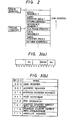
- Fig. 3(a) shows an instruction format for this processor.
- the instruction consists fundamentally of an operation word for designating a kind of operation, a register to be used, and an addressing mode or the like, and an expansion portion which gives data for address calculation. Depending upon the kind of addressing mode designated, however, the instruction format is not often provided with an expansion portion.
- Bits 11 to 9 of the operation word represent number of data register that holds data used as an operand for arithmetic operation.
- Another operand is designated by bits 5 to 0 of the operation word. That is, bits 2 to 0 represent number of register to which the reference will be made to obtain the operand.
- the processor contains 16 registers. Among them, there are eight data registers to store the operands, and there are eight other address registers to store addresses of operands on the memory device. These registers are designated by instruction to obtain operands.
- Bits 5 to 3 represent addressing modes.
- Fig. 3(b) shows the correspondence between bit patterns of bits 5 to 3 and addressing modes.
- the "data register” mode and the "address register” mode are those in which contents of the designated data register and address register serve as operands.
- the "address register indirect” mode is the one in which content of a designated address register is used as a memory address of operand on the memory device.
- the "post-increment” mode and the “pre-decrement” mode are fundamentally the same as the "address register indirect” mode, but differ in that they set the contents of the address registers to +1 and -1, respectively, just after and immediately before the operand is stored or fetched.
- the "address register indirect with displacement” mode is the one in which a value obtained by adding the content of expansion portion to the content of the designated address register, is used as a memory address of operand
- the "program counter indirect with displacement'! mode is the one in which a value obtained by adding the content of expansion portion to the address (content of the program counter) of the instruction, is used as a memory address of operand.
- the "absolute address” mode is the one in which content of the expansion portion is directly used as a memory address of operand.
- the stack access mode will be described below.
- the stack is realized by the combination of a portion of the main memory, a stack pointer and a frame pointer. That is, the content of the stack pointer is renewed successively, and the variable is successively stored in the main memory using the content of the stack pointer as an addresss of the main memory.
- the frame corresponding to the main routine When a subroutine is to be called from the main routine, the frame corresponding to the main routine must be switched to the frame corresponding to the subroutine. For this purpose, content of the stack pointer used in the main routine is copied onto the frame pointer. Further, content of the frame pointer up to that moment is stored at an address position on the main memory designated by the present frame pointer.
- Fig. 2 shows construction of such a stack which stores a local variable used for each subroutine when the procedure is to be executed, a saved register value for restoration at the outlet of the procedure, a return address from the procedure, a reference number for each procedure, and the value of the frame pointer (old frame pointer) at the time of starting the execution of procedure, in the order mentioned from the top of the stack on the main memory.
- the stack pointer designates the address of the top (head) of the stack
- the frame pointer designates the address where the value of the old frame pointer is stored. In the stack holding such data, the probability of access is high, as is that of repeated access.
- Access to the stack designates the frame pointer or the stack pointer, and is executed using any one of "address register indirect”, “post-increment”, “pre-decrement”, or “address register indirect with displacement” as an addressing mode. These modes of access to the stack are generally called stack access modes.
- the frame pointer is designated by setting bits 2 to 0 of instruction format of Fig. 3(a) to "110".
- the stack pointer is designated by setting bits 2 to 0 to "111". In the stack access mode, therefore, the low-order 6 bits of operation word assume any one of "010110”, "010111”, “011110”, “011111”, “100110”, “100111”, “101110”, or "101111".
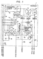
- FIG. 1 shows an embodiment of the present invention which utilizes a cache memory to access the stacked region.
- An instruction_control circuit 10 contains a register (IR) 11 for holding the operation word, decodes the instruction, and supplies a control signal into a processor 1 as well as to an external unit.
- a register group 13 consists of a set of the aforementioned eight data registers and eight address registers. One of the address registers is a frame pointer, and another one is a stack pointer. Operation of data for the operand and address calculation are executed by an arithmetic unit (ALU) 12, and the operated data is stored in a designated register in the register group 13, and the address value is stored in a memory address register (MAR) 15.
- ALU arithmetic unit
- a mode detection decoder 14 decodes the low-order 6 bits 113 of the register (IR) 11, and renders a signal 114 on if the stack access mode has been designated (i.e., if they pertain to any one of the aforementioned eight bit patterns).
- An associative memory 26 is used as the cache memory, and is referenced with the address as an index. If the data of the address is being held, the associative memory 26 sets the flip-flop 27 to render.a signal 118 on.
- Reference numeral 111 denotes a store operation signal
- 116 denotes a fetch operation signal
- 119 denotes an address value
- 120 denotes fetched data
- 121 denotes data to be stored
- 122 denotes the end signal of the operation of the main memory.
- the fetched data and instructions are temporarily stored in a read data register (RDR) 16, and the data to be stored are prepared in a write data register (WDR) 17.
- RDR read data register
- WDR write data register
- a selector 23 selects either the output of the associative memory 26 or fetched data 120 from memory as the data to be stored in the RDR 16, and a selector 28 selects either fetched data 120 from the memory or stores data 121 thereto as the data to be written onto the associative memory 26.
- a counter 24 designates an entry position for writing onto the associative memory 26.
- AND gates 19 to 21 and an OR gate 22 constitute a logic circuit for generating a cache write direction signal 115, while inverters 2 9, 33, delay circuit-34, AND gates 30,-32 and OR gate 31 constitute a logic circuit for generating a fetch operation signal 116. Functions of the AND gates 25, 35, and of the OR gate 18 will be described later together with the operation of the whole apparatus.
- the processor 1 is constructed as described above and is formed on a chip.
- the operand address is calculated by the ALU 12, set to the MAR 15, and is produced as a signal 119. Then, the instruction control circuit 10 turns the internal fetch direction signal 112 on to start the fetch.
- the operand address (signal 119) has been input to the associative memory 26. If there is the data of a corresponding address as a result of reference based upon the address value, the flip-flop 27 is latched to "1". If there exists no data, the flip-flop 27 is latched to "0".
- output signal 114 of the decoder 14 is on, so that the AND gate 30 is not turned on. Therefore, the fetch operation signal 116 is rendered on only when the AND gate 32 is turned on.
- the delay circuit 34 works to delay the signal 112 until reference of the associative memory 26 is finished.
- the signal 118 When the corresponding data exists in the associative memory 26, the signal 118 is rendered on, but the AND gate 32 is not turned on. Therefore, the signal 116 remains off. Namely, the memory does not perform a fetch. 'When the signal 116 is off, the selector 23 sends the data read from the associative memory 26 to the RDR 16. The signal 1 1 0 is rendered on by the function of AND gate 35 and OR gate 18, and the completion of the fetch is reported to the instruction control circuit 10 which latches the data to the RDR 16 to complete the fetch. Namely, in this case, only the reading of data is fetched from the associative memory 26.
- the signal 118 is rendered off. Therefore, after being delayed by the delay circuit 34, the AND gate 32 is turned on, and the fetch operation signal 116 is rendered on.
- the memory which is not shown reads the data of address indicated by signal 119, produces a signal 120, and then renders the signal 122 on.
- the signal 122 is rendered on, the signal 110 is rendered on via OR gate 18, and the completion of the fetch is reported to the instruction control circuit 10.
- the instruction control circuit.l0 works to latch the data to the RDR 16. At this moment, however, since the signal 116 is on, the selector 23 selects the signal 120; i.e., the data 120 read from the memory is latched to the RDR 16.
- the signal 114 When the fetch is to be effected in a mode other than the stack access mode, the signal 114 is rendered off. Therefore, as the signal 112 is rendered on, the fetch operation signal 116 is turned on readily via AND gate 30 and OR gate 31, and the memory initiates the read operation. When the operation for reading data from memory is completed, the signal 122 is rendered on, and the completion of fetch is reported to the instruction control circuit 10 via OR gate 18 and signal 110. The data 120 read from the memory is latched to the RDR 16 via selector 23 which is switched by signal 116. In this case, however, since the signal 114 is off, the signal 115 is not rendered on and the data is not written onto the associative memory 26. That is, the fetch operation in the mode other than the stack access mode is readily performed for the memory without regard to the associative memory 26.
- the instruction control circuit 10 first, sets a store address to MAR 15, sets the data to be stored to WDR 17, and then renders the signal 111 on to start the store operation.
- the memory writes the data on signal 121 onto the address indicated by signal 119.
- the associative memory 26 is referenced and the result is produced as signal 118.
- the memory renders the signal 122 on to inform the completion of operation.
- the signal 114 is on and the store operation signal 111 is on, too. Therefore, if the signal 122 is turned on, output of the AND gate 20 is turned on, the signal 115 is turned on via OR gate 22, and writing of data onto the associative memory 26 is directed.
- the signal 118 is off, and both the address and the data are written onto the entry indicated by the counter 24 of associative memory 26.
- the signal 118 is rendered on, and only the data is written onto the corresponding entry of the associative memory 26.
- the data stored in the memory are necessarily written onto the associative memory 26.
- the associative memory 26 does not contain filler any more, the data which is regarded to be least necessary is discarded and a new data is written thereon as in the conventional cache memory.
- Operation for storing data in a mode other than the stack access mode is the same as the operation for storing data in the stack access mode, except for the below-mentioned points. That is, in the case of a mode other than the stack access mode, the signal 114 is off. Therefore, output of the AND gate 20 is not turned on even when the finish of operation notice signal 122 is turned on.
- the signal 118 is on, i.e., when the associative memory 26 contains an address that is in agreement with the store address, however, the signal 115 is turned on via AND gate 21 and OR gate 22, and writing of only data onto the associative memory 26 is directed. This helps maintain the data held by the associative memory 26 to be in agreement with the data of a corresponding address on the memory.
- the cache memory is utilized for only those stacks from which the data written thereon are to be read out again immediately, or from which the data once read are to be read out again immediately. Compared with an ordinary cache system which utilizes cache memory for all data that are to be accessed, therefore, a high hit ratio can be obtained even with a cache memory having a small capacity.
- the embodiment deals with a system in which only those data that are to be accessed are copied onto the cache memory.
- the invention can also be adapted even to a system in which the data are copied with the block as a unit.
- the processor 1 is formed in a single chip, and the address prepared in the chip is supplied to the external main memory.
- the address prepared in the chip may differ from the address put to the memory outside the chip, and the address prepared in the chip is often called the logical address, and the address put to the memory outside the chip is often called physical address.
- mapping between the logical address and the physical address is performed by providing a particular hardware called an address mapping mechanism. Such a mapping mechanism has been widely known, and people skilled in the art may easily adopt it for the present invention.
- the cache memory is utilized for only those data that are utilized at an increased frequency. Therefore, it is possible to obtain a cache memory which exhibits a high hit ratio and a high efficiency in spite of its small capacity, and to enjoy the advantage of cache memory even with a very small processor.
- a high performance microprocessor can be realized with a small chip.
Landscapes
- Engineering & Computer Science (AREA)
- Theoretical Computer Science (AREA)
- Physics & Mathematics (AREA)
- General Engineering & Computer Science (AREA)
- General Physics & Mathematics (AREA)
- Memory System Of A Hierarchy Structure (AREA)
Abstract
Description
- The present invention relates to a cache memory control circuit.
- A cache memory works to reduce the time required for obtaining data, and is widely employed as means to enhance performance of a processor. A computer employing cache memory has been disclosed, for example, in "AFIPS", Vol. 45, pp. 749, 1976.
- In recent years, cache memory has been employed even in microprocessors, when required data has not been contained in the cache memory, the data or a data block containing the data must be fetched from the main memory. The fetching, however, is carried out requiring ordinary fetching time as well as reference time to determine whether the data is contained in the cache memory or not. Therefore, if the probability (hereinafter referred to as hit rate) in which the necessary data exists in the cache memory is low, it becomes difficult to enhance the performance as expected but rather the retrieval time turns out to be overhead and, in extreme cases, performance is often deteriorated. As for the instructions, in general, the same instruction is in many cases accessed many times since data is localized in a relatively small area. Therefore, a high hit ratio is obtained even with the cache memory of a relatively small capacity. In the case of an operand, however, the locality is relatively weak, so that a higt hit ratio is not effectively obtained unless the cache memory has a capacity which is relatively large. For this reason, even a minicomputer is usually provided with a cache memory having a capacity of about four kilobytes.
- However, in a very small processor such as a microprocessor, the time for sending and receiving data relative to an external-unit is considerably longer than the time in the chip. Therefore, it has been strongly desired to form a cache memory in the same chip as the CPU. With the current integration degree of LSIs, however, it is difficult to form a cache memory of a large capacity on the same chip as the CPU. At present, therefore, the capacity of about 500 bytes is a limit, Therefore, a contrivance is necessary to obtain a high hit rate even with the cache memory of a small capacity.
- The object of the present invention is to provide a cache memory which exhibits a high hit rate and an increased efficiency in spite of its small capacity, to make it possible to enjoy the advantage of cache memory even with a very small processor.
- The present invention is to utilize the cache memory only for those data that are to be utilized repeatedly. With the cache memory control circuit of the present invention, it can be determined whether memory access is directed to a particular region or not, as well as when the data is to be read out or written to the particular region depending upon the result of detection, the subject data is copied onto the cache memory, and when the data is to be read out from other regions, that data is immediately read out from the memory without waiting for the-reference of cache memory.
- By assigning the particular region for the data that are to be repeatedly used at a high percentage, it is possible to obtain a cache memory having good efficiency in spite of its small capacity. A representative example of such data is data in a "stack" in memory.
-
- Fig. 1 is a block diagram showing an embodiment of the present invention;
- Fig. 2 is-a diagram which schematically illustrates a stack; and
- Fig. 3 is a diagram showing an instruction format of the embodiment of Fig. 1 in relation to the access modes.
- A preferred embodiment of the present invention will be described below.
- Instruction for the control apparatus of the embodiment will first be described below and the apparatus will be described thereafter.
- Fig. 3(a) shows an instruction format for this processor. The instruction consists fundamentally of an operation word for designating a kind of operation, a register to be used, and an addressing mode or the like, and an expansion portion which gives data for address calculation. Depending upon the kind of addressing mode designated, however, the instruction format is not often provided with an expansion portion.
Bits 11 to 9 of the operation word represent number of data register that holds data used as an operand for arithmetic operation. Another operand is designated bybits 5 to 0 of the operation word. That is,bits 2 to 0 represent number of register to which the reference will be made to obtain the operand. As will be described later, the processor contains 16 registers. Among them, there are eight data registers to store the operands, and there are eight other address registers to store addresses of operands on the memory device. These registers are designated by instruction to obtain operands.Bits 5 to 3 represent addressing modes. - Fig. 3(b) shows the correspondence between bit patterns of
bits 5 to 3 and addressing modes. In Fig. 3(b), the "data register" mode and the "address register" mode are those in which contents of the designated data register and address register serve as operands. - The "address register indirect" mode is the one in which content of a designated address register is used as a memory address of operand on the memory device. The "post-increment" mode and the "pre-decrement" mode are fundamentally the same as the "address register indirect" mode, but differ in that they set the contents of the address registers to +1 and -1, respectively, just after and immediately before the operand is stored or fetched.
- The "address register indirect with displacement" mode is the one in which a value obtained by adding the content of expansion portion to the content of the designated address register, is used as a memory address of operand, and the "program counter indirect with displacement'! mode is the one in which a value obtained by adding the content of expansion portion to the address (content of the program counter) of the instruction, is used as a memory address of operand. The "absolute address" mode is the one in which content of the expansion portion is directly used as a memory address of operand.
- The stack access mode will be described below.
- Most programs are written in a high-level language, and have stack as its data structure. When a subroutine is used, in particular, variables used in the main routine and variables in the subroutine are stored in the stack as separate masses. Such masses are called frames which are provided for each of the routines.
- In the case of a small processor, in particular, the stack is realized by the combination of a portion of the main memory, a stack pointer and a frame pointer. That is, the content of the stack pointer is renewed successively, and the variable is successively stored in the main memory using the content of the stack pointer as an adress of the main memory.
- When a subroutine is to be called from the main routine, the frame corresponding to the main routine must be switched to the frame corresponding to the subroutine. For this purpose, content of the stack pointer used in the main routine is copied onto the frame pointer. Further, content of the frame pointer up to that moment is stored at an address position on the main memory designated by the present frame pointer.
- Fig. 2 shows construction of such a stack which stores a local variable used for each subroutine when the procedure is to be executed, a saved register value for restoration at the outlet of the procedure, a return address from the procedure, a reference number for each procedure, and the value of the frame pointer (old frame pointer) at the time of starting the execution of procedure, in the order mentioned from the top of the stack on the main memory. The stack pointer designates the address of the top (head) of the stack, and the frame pointer designates the address where the value of the old frame pointer is stored. In the stack holding such data, the probability of access is high, as is that of repeated access.
- Access to the stack designates the frame pointer or the stack pointer, and is executed using any one of "address register indirect", "post-increment", "pre-decrement", or "address register indirect with displacement" as an addressing mode. These modes of access to the stack are generally called stack access modes.
- In this processor, two address registers are assigned to the frame pointer and to the stack pointer, respectively, among eight address registers. That is, the frame pointer is designated by setting
bits 2 to 0 of instruction format of Fig. 3(a) to "110". Further, the stack pointer is designated by settingbits 2 to 0 to "111". In the stack access mode, therefore, the low-order 6 bits of operation word assume any one of "010110", "010111", "011110", "011111", "100110", "100111", "101110", or "101111". - Construction of the apparatus will be described below in detail.
- Fig. 1 shows an embodiment of the present invention which utilizes a cache memory to access the stacked region. An
instruction_control circuit 10 contains a register (IR) 11 for holding the operation word, decodes the instruction, and supplies a control signal into aprocessor 1 as well as to an external unit. Aregister group 13 consists of a set of the aforementioned eight data registers and eight address registers. One of the address registers is a frame pointer, and another one is a stack pointer. Operation of data for the operand and address calculation are executed by an arithmetic unit (ALU) 12, and the operated data is stored in a designated register in theregister group 13, and the address value is stored in a memory address register (MAR) 15. Amode detection decoder 14 decodes the low-order 6bits 113 of the register (IR) 11, and renders asignal 114 on if the stack access mode has been designated (i.e., if they pertain to any one of the aforementioned eight bit patterns). Anassociative memory 26 is used as the cache memory, and is referenced with the address as an index. If the data of the address is being held, theassociative memory 26 sets the flip-flop 27 to render.asignal 118 on.Reference numeral 111 denotes a store operation signal, 116 denotes a fetch operation signal, 119 denotes an address value, 120 denotes fetched data, 121 denotes data to be stored, and 122 denotes the end signal of the operation of the main memory. These signals are sent to a memory that is not shown. The fetched data and instructions are temporarily stored in a read data register (RDR) 16, and the data to be stored are prepared in a write data register (WDR) 17. Aselector 23 selects either the output of theassociative memory 26 orfetched data 120 from memory as the data to be stored in theRDR 16, and aselector 28 selects eitherfetched data 120 from the memory orstores data 121 thereto as the data to be written onto theassociative memory 26. Acounter 24 designates an entry position for writing onto theassociative memory 26. ANDgates 19 to 21 and anOR gate 22 constitute a logic circuit for generating a cache write direction signal 115, whileinverters gates 30,-32 andOR gate 31 constitute a logic circuit for generating a fetchoperation signal 116. Functions of the ANDgates OR gate 18 will be described later together with the operation of the whole apparatus. - The
processor 1 is constructed as described above and is formed on a chip. - Operation of the apparatus will be described below with reference to the cases where the data is to be fetched in the stack access mode, where the data is to be fetched in a mode other than the stack access mode, where the data is to be stored in the stack access mode, and where the data is to be stored in a mode other than the stack access mode. In the following description, it should be presumed that the operation word of each instruction is set to register 11.
- When the operand is to be fetched, the operand address is calculated by the
ALU 12, set to theMAR 15, and is produced as asignal 119. Then, theinstruction control circuit 10 turns the internal fetch direction signal 112 on to start the fetch. The operand address (signal 119) has been input to theassociative memory 26. If there is the data of a corresponding address as a result of reference based upon the address value, the flip-flop 27 is latched to "1". If there exists no data, the flip-flop 27 is latched to "0". In the stack access mode,output signal 114 of thedecoder 14 is on, so that the ANDgate 30 is not turned on. Therefore, the fetchoperation signal 116 is rendered on only when the ANDgate 32 is turned on. Thedelay circuit 34 works to delay thesignal 112 until reference of theassociative memory 26 is finished. - When the corresponding data exists in the
associative memory 26, thesignal 118 is rendered on, but the ANDgate 32 is not turned on. Therefore, thesignal 116 remains off. Namely, the memory does not perform a fetch. 'When thesignal 116 is off, theselector 23 sends the data read from theassociative memory 26 to theRDR 16. Thesignal 110 is rendered on by the function of ANDgate 35 andOR gate 18, and the completion of the fetch is reported to theinstruction control circuit 10 which latches the data to theRDR 16 to complete the fetch. Namely, in this case, only the reading of data is fetched from theassociative memory 26. - When the corresponding data does not exist in the
associative memory 26, thesignal 118 is rendered off. Therefore, after being delayed by thedelay circuit 34, the ANDgate 32 is turned on, and the fetchoperation signal 116 is rendered on. As thesignal 116 is rendered on, the memory which is not shown reads the data of address indicated bysignal 119, produces asignal 120, and then renders thesignal 122 on. As thesignal 122 is rendered on, thesignal 110 is rendered on viaOR gate 18, and the completion of the fetch is reported to theinstruction control circuit 10. The instruction control circuit.l0 works to latch the data to theRDR 16. At this moment, however, since thesignal 116 is on, theselector 23 selects thesignal 120; i.e., thedata 120 read from the memory is latched to theRDR 16. As thesignal 122 is rendered on, output of the ANDgate 19 is rendered on since the operation is in the stack access mode, i.e., since thesignal 114 is on. Therefore, the cache write direction signal 115 is rendered on viaOR gate 22, and write operation is instructed to theassociative memory 26 which is receiving the signal 120 (output of memory) as write data that is switched bysignal 116 via theselector 28. If the write operation is instructed with thesignal 118 being off, address (signal 119) and data (signal 120) are written onto the entry ofassociative memory 26 indicated by thecounter 24. The value ofcounter 24 is counted up since the output of ANDgate 25 is rendered on by thesignal 115 and by the output ofinvertor 33. Thus, when the corresponding data of address does not exist in theassociative memory 26 with the fetch being effected in the stack access mode, the data and address read from the memory are written onto theassociative memory 26. - When the fetch is to be effected in a mode other than the stack access mode, the
signal 114 is rendered off. Therefore, as thesignal 112 is rendered on, the fetchoperation signal 116 is turned on readily via ANDgate 30 andOR gate 31, and the memory initiates the read operation. When the operation for reading data from memory is completed, thesignal 122 is rendered on, and the completion of fetch is reported to theinstruction control circuit 10 viaOR gate 18 and signal 110. Thedata 120 read from the memory is latched to theRDR 16 viaselector 23 which is switched bysignal 116. In this case, however, since thesignal 114 is off, thesignal 115 is not rendered on and the data is not written onto theassociative memory 26. That is, the fetch operation in the mode other than the stack access mode is readily performed for the memory without regard to theassociative memory 26. - Described below is the operation when the data is to be stored in the stack access mode. When the data is to be stored, the
instruction control circuit 10, first, sets a store address to MAR 15, sets the data to be stored toWDR 17, and then renders thesignal 111 on to start the store operation. As thesignal 111 is turned on, the memory writes the data onsignal 121 onto the address indicated bysignal 119. In parallel with this, theassociative memory 26 is referenced and the result is produced assignal 118. When the operation for writing data is finished, the memory renders thesignal 122 on to inform the completion of operation. At this moment, thesignal 114 is on and thestore operation signal 111 is on, too. Therefore, if thesignal 122 is turned on, output of the ANDgate 20 is turned on, thesignal 115 is turned on viaOR gate 22, and writing of data onto theassociative memory 26 is directed. - Here, when the
associative memory 26 contains no address that is in agreement with the write address, thesignal 118 is off, and both the address and the data are written onto the entry indicated by thecounter 24 ofassociative memory 26. On the other hand, when theassociative memory 26 contains an address that is in agreement with the write address, thesignal 118 is rendered on, and only the data is written onto the corresponding entry of theassociative memory 26. Thus, when the data is to be stored in the stack access mode, the data stored in the memory are necessarily written onto theassociative memory 26. When theassociative memory 26 does not contain filler any more, the data which is regarded to be least necessary is discarded and a new data is written thereon as in the conventional cache memory. - Operation for storing data in a mode other than the stack access mode is the same as the operation for storing data in the stack access mode, except for the below-mentioned points. That is, in the case of a mode other than the stack access mode, the
signal 114 is off. Therefore, output of the ANDgate 20 is not turned on even when the finish ofoperation notice signal 122 is turned on. When thesignal 118 is on, i.e., when theassociative memory 26 contains an address that is in agreement with the store address, however, thesignal 115 is turned on via ANDgate 21 andOR gate 22, and writing of only data onto theassociative memory 26 is directed. This helps maintain the data held by theassociative memory 26 to be in agreement with the data of a corresponding address on the memory. - According to this embodiment as described above, the cache memory is utilized for only those stacks from which the data written thereon are to be read out again immediately, or from which the data once read are to be read out again immediately. Compared with an ordinary cache system which utilizes cache memory for all data that are to be accessed, therefore, a high hit ratio can be obtained even with a cache memory having a small capacity.
- The embodiment deals with a system in which only those data that are to be accessed are copied onto the cache memory. The invention, however, can also be adapted even to a system in which the data are copied with the block as a unit.
- The above-mentioned embodiment has dealt with the case where the
processor 1 is directly connected to the memory. Here, however, an address conversion mechanism may be provided between theprocessor 1 and the memory. - As described above, the
processor 1 is formed in a single chip, and the address prepared in the chip is supplied to the external main memory. In some of the currently proposed systems, however, the address prepared in the chip may differ from the address put to the memory outside the chip, and the address prepared in the chip is often called the logical address, and the address put to the memory outside the chip is often called physical address. In general, mapping between the logical address and the physical address is performed by providing a particular hardware called an address mapping mechanism. Such a mapping mechanism has been widely known, and people skilled in the art may easily adopt it for the present invention. - With the present invention, the cache memory is utilized for only those data that are utilized at an increased frequency. Therefore, it is possible to obtain a cache memory which exhibits a high hit ratio and a high efficiency in spite of its small capacity, and to enjoy the advantage of cache memory even with a very small processor. A high performance microprocessor can be realized with a small chip.
Claims (11)
wherein said instruction control means (10) controls to execute said instruction relying upon the operand read from said first or second memory means.
Applications Claiming Priority (2)
| Application Number | Priority Date | Filing Date | Title |
|---|---|---|---|
| JP59180434A JPH0630075B2 (en) | 1984-08-31 | 1984-08-31 | Data processing device having cache memory |
| JP180434/84 | 1984-08-31 |
Publications (2)
| Publication Number | Publication Date |
|---|---|
| EP0173981A2 true EP0173981A2 (en) | 1986-03-12 |
| EP0173981A3 EP0173981A3 (en) | 1989-05-31 |
Family
ID=16083177
Family Applications (1)
| Application Number | Title | Priority Date | Filing Date |
|---|---|---|---|
| EP85110962A Withdrawn EP0173981A3 (en) | 1984-08-31 | 1985-08-30 | Cache memory control circuit |
Country Status (4)
| Country | Link |
|---|---|
| US (1) | US4937738A (en) |
| EP (1) | EP0173981A3 (en) |
| JP (1) | JPH0630075B2 (en) |
| KR (1) | KR920005292B1 (en) |
Cited By (7)
| Publication number | Priority date | Publication date | Assignee | Title |
|---|---|---|---|---|
| EP0382396A3 (en) * | 1989-02-08 | 1991-11-27 | Hitachi, Ltd. | Program memory buffer for processor |
| EP0405318A3 (en) * | 1989-06-20 | 1991-11-27 | Nec Corporation | Microprocessor having cash bypass signal terminal |
| GB2247546A (en) * | 1990-08-31 | 1992-03-04 | Sun Microsystems Inc | Predictive caching system |
| EP0395559A3 (en) * | 1989-04-25 | 1992-06-03 | International Business Machines Corporation | Distributed cache dram chip |
| US5257359A (en) * | 1989-02-08 | 1993-10-26 | Hitachi Microsystems, Inc. | Instruction cache buffer with program-flow control |
| EP0779581A3 (en) * | 1995-12-13 | 1997-07-02 | International Business Machines Corporation | CPU with cache memory |
| EP1434136A1 (en) * | 2002-12-27 | 2004-06-30 | Siemens Aktiengesellschaft | Microprocessor with cache memory and secondary memory, and method for programming such a microprocessor |
Families Citing this family (18)
| Publication number | Priority date | Publication date | Assignee | Title |
|---|---|---|---|---|
| JP2748359B2 (en) * | 1986-08-01 | 1998-05-06 | 株式会社日立製作所 | Parallel processor system and method for executing a plurality of instruction sequences by parallel processor |
| JP2881760B2 (en) * | 1986-12-24 | 1999-04-12 | 日本精工株式会社 | A composite transmission for a vehicle including a continuously variable transmission and a stepped transmission |
| JP2617974B2 (en) * | 1988-03-08 | 1997-06-11 | 富士通株式会社 | Data processing device |
| JP2695017B2 (en) * | 1989-11-08 | 1997-12-24 | 富士通株式会社 | Data transfer method |
| DE69025302T2 (en) * | 1989-12-22 | 1996-10-02 | Digital Equipment Corp | Heavy duty grid buffer and cache array |
| EP0449369B1 (en) * | 1990-03-27 | 1998-07-29 | Koninklijke Philips Electronics N.V. | A data processing system provided with a performance enhancing instruction cache |
| DE69128741T2 (en) * | 1990-05-18 | 1998-07-16 | Koninkl Philips Electronics Nv | Multi-level instruction cache and method of use therefor |
| US5249281A (en) * | 1990-10-12 | 1993-09-28 | Lsi Logic Corporation | Testable ram architecture in a microprocessor having embedded cache memory |
| US5625793A (en) * | 1991-04-15 | 1997-04-29 | International Business Machines Corporation | Automatic cache bypass for instructions exhibiting poor cache hit ratio |
| WO1995032466A1 (en) * | 1994-05-19 | 1995-11-30 | Vlsi Technology, Inc. | Flexible register mapping scheme |
| JPH0824098A (en) * | 1994-07-20 | 1996-01-30 | Hakohide Shiki Seisakusho:Kk | Frame frame component member, frame frame using the same, and manufacturing method thereof |
| US5890216A (en) * | 1995-04-21 | 1999-03-30 | International Business Machines Corporation | Apparatus and method for decreasing the access time to non-cacheable address space in a computer system |
| US20030196072A1 (en) * | 2002-04-11 | 2003-10-16 | Chinnakonda Murali S. | Digital signal processor architecture for high computation speed |
| US7454585B2 (en) | 2005-12-22 | 2008-11-18 | International Business Machines Corporation | Efficient and flexible memory copy operation |
| US7506132B2 (en) * | 2005-12-22 | 2009-03-17 | International Business Machines Corporation | Validity of address ranges used in semi-synchronous memory copy operations |
| US7484062B2 (en) * | 2005-12-22 | 2009-01-27 | International Business Machines Corporation | Cache injection semi-synchronous memory copy operation |
| EP1919067B1 (en) * | 2006-10-31 | 2009-04-29 | Infineon Technologies Austria AG | Control circuit for a switch in a switched mode power supply with burst mode |
| JP6155723B2 (en) | 2013-03-18 | 2017-07-05 | 富士通株式会社 | Radar apparatus and program |
Family Cites Families (19)
| Publication number | Priority date | Publication date | Assignee | Title |
|---|---|---|---|---|
| US4075686A (en) * | 1976-12-30 | 1978-02-21 | Honeywell Information Systems Inc. | Input/output cache system including bypass capability |
| US4357656A (en) * | 1977-12-09 | 1982-11-02 | Digital Equipment Corporation | Method and apparatus for disabling and diagnosing cache memory storage locations |
| US4189770A (en) * | 1978-03-16 | 1980-02-19 | International Business Machines Corporation | Cache bypass control for operand fetches |
| JPS54128634A (en) * | 1978-03-30 | 1979-10-05 | Toshiba Corp | Cash memory control system |
| JPS54128640A (en) * | 1978-03-30 | 1979-10-05 | Toshiba Corp | Control system for cash memory |
| US4338663A (en) * | 1978-10-25 | 1982-07-06 | Digital Equipment Corporation | Calling instructions for a data processing system |
| US4298929A (en) * | 1979-01-26 | 1981-11-03 | International Business Machines Corporation | Integrated multilevel storage hierarchy for a data processing system with improved channel to memory write capability |
| JPS563485A (en) * | 1979-06-20 | 1981-01-14 | Nec Corp | Buffer memory device |
| JPS56143583A (en) * | 1980-04-11 | 1981-11-09 | Toshiba Corp | Buffer memory control system |
| US4398243A (en) * | 1980-04-25 | 1983-08-09 | Data General Corporation | Data processing system having a unique instruction processor system |
| US4382278A (en) * | 1980-06-05 | 1983-05-03 | Texas Instruments Incorporated | Hierarchial memory system with microcommand memory and pointer register mapping virtual CPU registers in workspace cache #4 and main memory cache |
| JPS57114950A (en) * | 1981-01-08 | 1982-07-17 | Nippon Telegr & Teleph Corp <Ntt> | Loop processing system for program controller |
| US4500954A (en) * | 1981-10-15 | 1985-02-19 | International Business Machines Corporation | Cache bypass system with post-block transfer directory examinations for updating cache and/or maintaining bypass |
| US4530049A (en) * | 1982-02-11 | 1985-07-16 | At&T Bell Laboratories | Stack cache with fixed size stack frames |
| US4597044A (en) * | 1982-10-14 | 1986-06-24 | Honeywell Information Systems, Inc. | Apparatus and method for providing a composite descriptor in a data processing system |
| JPS60500187A (en) * | 1982-12-30 | 1985-02-07 | インタ−ナシヨナル・ビジネス・マシ−ンズ・コ−ポレ−シヨン | data processing system |
| US4626988A (en) * | 1983-03-07 | 1986-12-02 | International Business Machines Corporation | Instruction fetch look-aside buffer with loop mode control |
| US4635194A (en) * | 1983-05-02 | 1987-01-06 | International Business Machines Corporation | Instruction buffer bypass apparatus |
| US4669043A (en) * | 1984-02-17 | 1987-05-26 | Signetics Corporation | Memory access controller |
-
1984
- 1984-08-31 JP JP59180434A patent/JPH0630075B2/en not_active Expired - Lifetime
-
1985
- 1985-08-09 KR KR1019850005746A patent/KR920005292B1/en not_active Expired
- 1985-08-23 US US06/768,572 patent/US4937738A/en not_active Expired - Fee Related
- 1985-08-30 EP EP85110962A patent/EP0173981A3/en not_active Withdrawn
Cited By (11)
| Publication number | Priority date | Publication date | Assignee | Title |
|---|---|---|---|---|
| EP0382396A3 (en) * | 1989-02-08 | 1991-11-27 | Hitachi, Ltd. | Program memory buffer for processor |
| US5257359A (en) * | 1989-02-08 | 1993-10-26 | Hitachi Microsystems, Inc. | Instruction cache buffer with program-flow control |
| EP0395559A3 (en) * | 1989-04-25 | 1992-06-03 | International Business Machines Corporation | Distributed cache dram chip |
| US5421000A (en) * | 1989-04-25 | 1995-05-30 | International Business Machines Corp. | Memory subsystem having a static row memory and a dynamic RAM |
| EP0405318A3 (en) * | 1989-06-20 | 1991-11-27 | Nec Corporation | Microprocessor having cash bypass signal terminal |
| US5247639A (en) * | 1989-06-20 | 1993-09-21 | Nec Corporation | Microprocessor having cache bypass signal terminal |
| GB2247546A (en) * | 1990-08-31 | 1992-03-04 | Sun Microsystems Inc | Predictive caching system |
| US5287487A (en) * | 1990-08-31 | 1994-02-15 | Sun Microsystems, Inc. | Predictive caching method and apparatus for generating a predicted address for a frame buffer |
| GB2247546B (en) * | 1990-08-31 | 1995-03-01 | Sun Microsystems Inc | Method and apparatus for predictive caching |
| EP0779581A3 (en) * | 1995-12-13 | 1997-07-02 | International Business Machines Corporation | CPU with cache memory |
| EP1434136A1 (en) * | 2002-12-27 | 2004-06-30 | Siemens Aktiengesellschaft | Microprocessor with cache memory and secondary memory, and method for programming such a microprocessor |
Also Published As
| Publication number | Publication date |
|---|---|
| US4937738A (en) | 1990-06-26 |
| EP0173981A3 (en) | 1989-05-31 |
| JPS6159554A (en) | 1986-03-27 |
| JPH0630075B2 (en) | 1994-04-20 |
| KR920005292B1 (en) | 1992-06-29 |
| KR860002049A (en) | 1986-03-26 |
Similar Documents
| Publication | Publication Date | Title |
|---|---|---|
| US4937738A (en) | Data processing system which selectively bypasses a cache memory in fetching information based upon bit information of an instruction | |
| US5247639A (en) | Microprocessor having cache bypass signal terminal | |
| US6779102B2 (en) | Data processor capable of executing an instruction that makes a cache memory ineffective | |
| JP2678183B2 (en) | Digital processor controller and method for runtime memory allocation | |
| EP0320098B1 (en) | Jump prediction | |
| US4912635A (en) | System for reexecuting branch instruction without fetching by storing target instruction control information | |
| JPS58102381A (en) | Buffer memory | |
| EP0118828A2 (en) | Instruction fetch apparatus and method of operating same | |
| JPH08328958A (en) | Instruction cache, cache memory device and method thereof | |
| KR910001314B1 (en) | How virtual memory is used in data processing systems | |
| US5226132A (en) | Multiple virtual addressing using/comparing translation pairs of addresses comprising a space address and an origin address (sto) while using space registers as storage devices for a data processing system | |
| US5206945A (en) | Single-chip pipeline processor for fetching/flushing instruction/data caches in response to first/second hit/mishit signal respectively detected in corresponding to their logical addresses | |
| US5463760A (en) | Break function in-circuit emulator for a microprocessor with a cache memory | |
| US5455925A (en) | Data processing device for maintaining coherency of data stored in main memory, external cache memory and internal cache memory | |
| EP0471888B1 (en) | Microprocessor for enhancing initiation of instruction execution after the execution of conditional branch instruction | |
| JPH0519176B2 (en) | ||
| US5012410A (en) | Data processor with instruction cache memory | |
| JPS6032220B2 (en) | information processing equipment | |
| JP2586160B2 (en) | Address translation mechanism | |
| JPS61136145A (en) | Cash memory control circuit | |
| JP2694076B2 (en) | Storage unit control device | |
| JPH077355B2 (en) | Information processing equipment | |
| JP2759952B2 (en) | Cache memory | |
| JPH06243045A (en) | Cache memory | |
| JPS58214947A (en) | Information processor |
Legal Events
| Date | Code | Title | Description |
|---|---|---|---|
| PUAI | Public reference made under article 153(3) epc to a published international application that has entered the european phase |
Free format text: ORIGINAL CODE: 0009012 |
|
| AK | Designated contracting states |
Kind code of ref document: A2 Designated state(s): DE FR GB IT |
|
| PUAL | Search report despatched |
Free format text: ORIGINAL CODE: 0009013 |
|
| AK | Designated contracting states |
Kind code of ref document: A3 Designated state(s): DE FR GB IT |
|
| 17P | Request for examination filed |
Effective date: 19891128 |
|
| RAP1 | Party data changed (applicant data changed or rights of an application transferred) |
Owner name: HITACHI MICROCOMPUTER SYSTEM LTD. Owner name: HITACHI, LTD. |
|
| 17Q | First examination report despatched |
Effective date: 19911011 |
|
| STAA | Information on the status of an ep patent application or granted ep patent |
Free format text: STATUS: THE APPLICATION IS DEEMED TO BE WITHDRAWN |
|
| 18D | Application deemed to be withdrawn |
Effective date: 19920222 |
|
| RIN1 | Information on inventor provided before grant (corrected) |
Inventor name: UCHIYAMA, KUNIO Inventor name: AIMOTO, TAKESHI Inventor name: NISHIMUKAI, TADAHIKO Inventor name: HASEGAWA, ATSUSHI |