EP0168023B1 - Dispositif opto-électronique de détection de passage d'objets - Google Patents
Dispositif opto-électronique de détection de passage d'objets Download PDFInfo
- Publication number
- EP0168023B1 EP0168023B1 EP85108473A EP85108473A EP0168023B1 EP 0168023 B1 EP0168023 B1 EP 0168023B1 EP 85108473 A EP85108473 A EP 85108473A EP 85108473 A EP85108473 A EP 85108473A EP 0168023 B1 EP0168023 B1 EP 0168023B1
- Authority
- EP
- European Patent Office
- Prior art keywords
- cavity
- plate
- opto
- case
- flap
- Prior art date
- Legal status (The legal status is an assumption and is not a legal conclusion. Google has not performed a legal analysis and makes no representation as to the accuracy of the status listed.)
- Expired
Links
Images



Classifications
-
- G—PHYSICS
- G01—MEASURING; TESTING
- G01V—GEOPHYSICS; GRAVITATIONAL MEASUREMENTS; DETECTING MASSES OR OBJECTS; TAGS
- G01V8/00—Prospecting or detecting by optical means
- G01V8/10—Detecting, e.g. by using light barriers
- G01V8/12—Detecting, e.g. by using light barriers using one transmitter and one receiver
-
- G—PHYSICS
- G02—OPTICS
- G02B—OPTICAL ELEMENTS, SYSTEMS OR APPARATUS
- G02B6/00—Light guides; Structural details of arrangements comprising light guides and other optical elements, e.g. couplings
- G02B6/24—Coupling light guides
- G02B6/42—Coupling light guides with opto-electronic elements
- G02B6/4201—Packages, e.g. shape, construction, internal or external details
- G02B6/4219—Mechanical fixtures for holding or positioning the elements relative to each other in the couplings; Alignment methods for the elements, e.g. measuring or observing methods especially used therefor
- G02B6/4236—Fixing or mounting methods of the aligned elements
-
- G—PHYSICS
- G02—OPTICS
- G02B—OPTICAL ELEMENTS, SYSTEMS OR APPARATUS
- G02B6/00—Light guides; Structural details of arrangements comprising light guides and other optical elements, e.g. couplings
- G02B6/24—Coupling light guides
- G02B6/42—Coupling light guides with opto-electronic elements
- G02B6/4201—Packages, e.g. shape, construction, internal or external details
- G02B6/4246—Bidirectionally operating package structures
Definitions
- the present invention relates to opto-electronic devices for detecting the passage of objects, in particular to those intended to equip automatic processing machines, such as in particular mail processing machines.
- the optical detectors are in known manner based either on a detection of the cut of the light beam emitted by a light source, during the passage of the object, or on a detection of the light beam coming from the source and returned to a receiver during the passage of the object.
- the source and the receiver are mounted face to face on one side and the other of the path of travel of the objects; in those operating according to the second mode, the source and the receiver are arranged side by side, on the same side of the path of travel of the objects.
- electronic control circuits are associated with the light source to allow a differentiation between the light emitted by the source and the ambient light.
- These circuits can comprise an oscillator with constant duty cycle, of fixed oscillation frequency of the order of 20 k Hertz, driving a power stage controlling an emissive diode in the visible range, which constitutes the light source.
- electronic circuits for processing the received signal are associated with the receiver, consisting of a photodiode, for the purpose of detecting it and then comparing it with a fixed or variable reference signal.
- These latter circuits may include a current / voltage converter of the signal from the receiving photodiode followed by a voltage amplifier, a high pass type filter of the amplified signal, an integrator type detector ensuring the detection of variation in the level of the signal received during the passage of the object to be detected, then a comparator and a signal output stage.
- These electronic circuits for controlling the diode and for processing the signal received by the photodiode can advantageously be grouped, with the diode and the photodiode, in a box equipped with optical conduits passing through it.
- These optical conduits are, when the equipment is housed in the factory, coupled to the diode and to the photodiode respectively, fixed on the walls of the housing which they pass through and set to a suitable length preset to ensure, in the defined conditions of use of the resulting final sensor, the connection between the equipment inside the housing and the points opposite or side by side for detecting the passage of objects.
- Such a sensor or the similar sensors entering an automated machine receive their power supply by electric cable; their electrical output signal is transmitted by individual electrical cable to an operating circuit mounted on a printed circuit board, from which the automatic control of the machine is ensured.
- their location in an automated machine is definitively conditioned by the length given to the optical conduits.
- the present invention relates to an opto-electronic device for detecting the passage of objects, for a machine with automatic control from these detections, retaining in particular the known principle of positioning the transceiver unit at a distance from the passage detection points of objects, by using optical conduits, but on the one hand avoiding any problem relating to the location of the device in a machine, linked to the length which was given to the optical conduits and on the other hand having a design allowing the elimination of electrical wiring necessary for the connection of each device to the operating circuit of the detection signals and to its power supply, so as to constitute a compact industrial device of very easy use.
- the subject of the present invention is therefore an opto-electronic device for detecting the passage of objects, with opto-electronic equipment mounted in a housing and coupled to optical fibers leaving the housing, characterized in that said opto-electronic equipment is carried by the same plate and that said housing is constituted by a body in one piece comprising a cavity in a so-called main part, constituting the housing of said plate and equipped with means for positioning and holding said plate, a side, said front side, a front end portion bordering said cavity at the front and equipped with passages opening into said cavity for said fibers and wire clamps for holding these fibers and, opposite, forming the end rear, a foldable flap defining the access of said plate into the cavity and ensuring its blocking.
- the 'wafer carries electric pins connected to said opto-electronic equipment which it wears and the free ends of which extend beyond the bottom of said housing, for direct racking of said device on a printed circuit board.
- the electronic circuit of the equipment will be integrated on the wafer for its miniaturization while the diode and the photodiode-entering the equipment will be mounted on the same side at the end of the wafer and connected to the circuit.
- the resulting device will be treated as a discrete component for mounting on a printed circuit board carrying the operating circuit.
- the opto-electronic device illustrated as it will advantageously be used in practice, is in the form of a box 1 containing the non-opto-electronic equipment visible from the device and resting on a printed circuit board 2, to which it is fixed by a pair of screws 3 and 4.
- This printed circuit board 2 constitutes a circuit board for processing the electrical signals produced by the opto-device electronics which are connected to it by electrical pins 5 exiting from the housing 1 and soldered to the printed circuit of the card 2, by which the opto-electronic device receives its power supply and transmits the electrical signals which it produces.
- This housing 1 is itself formed of a main part 10 substantially parallelepiped extending on one side said front side by a front end portion 50.
- the end portion 50 has its upper face in notch below the level of the upper face of the main part 10 and its side faces set back on those of the main part, the lower edges of the side walls of these two parts 10 and 50 being at the same level.
- the front end part 50 has a horizontal slot 51, substantially one third of its height from its upper wall. It receives, at the level of the slot 51, the ends of two sheathed optical fibers 6 and 7 which are held there by a nut 8 of a clamping system for its two parts defined on either side of the slot, forming wire clamp in this end part made elastically deformable.
- the screws 3 and 4 are inserted, for one of them 3, in the terminal part 50 between the bottom of the slot 51 which it has the main part 10 and, for the other 4, in the wall of the main part 10, opposite the front end part and called the rear wall, having for this purpose, externally, a middle rib 11 with rounded outline, on his height.
- FIGs 3, 4, 5 and 6 there is illustrated the housing 1 for receiving the optoelectronic equipment mounted entirely on the same wafer and the assembly of which constitutes the optoelectronic device.
- This housing 1 is constituted by a body in one piece made of plastic and directly obtained from molding.
- the main part 10 defines a cavity 20 open on the bottom of the housing 1.
- This main part 10 is in the form of a plate 12 bordered laterally by the front end part 50 and two flanges 13 and 14, which delimit on three sides the cavity 20.
- this plate 12 projects over the two flanges 13 and 14 and has on its internal face a groove 15 which delimits a terminal portion forming a flap 16 which can be folded down around the axis XX ( FIG. 3) for the constitution, as shown diagrammatically by the arrow F (FIG. 4), of the fourth side wall of the cavity 20, at the rear end of the housing 1.
- This flap 16 can be snapped onto the adjacent edges of the two flanges 13 and 14.
- each of the two vertical edges of these flanges forms a latching tab, such as 17, parallel to the flange which carries it but recessed on this flange towards the inside of the cavity, which ends in a boss 18 in relief towards the outside of the cavity.
- the flap 16 has, on the internal face of the plate 12 to which it belongs, two flanges ending in two rounded bosses such as 19 along its two edges, capable of engaging behind the bosses 18 of the tabs hanging 17.
- the front end portion 50 forms a notch substantially at half the width of the cavity, extending over a short distance towards the interior of the cavity by constituting 'before or at the end of the cavity a vertical partition 21 substantially median.
- This partition 21 and the portions of the flanges 13 and 14 opposite this partition define between them two vertical compartments 22 and 23 having, on the front end portion 50, their offset bottom.
- the compartmentalized end or front of the cavity 20 is of width less than that of the cavity itself but greater than that of the front end portion 50.
- Two inclined faces 24 and 34 and 25 and 35 form externally on one side and on the other these transitions, while inside the cavity 20, at the end of the partition 21 a shoulder such as 26 on each of the flanges catches up with the transition between the compartmentalized end of the cavity and the cavity itself, giving increased thickness to the flanges at this level.
- the end of the partition 21 has, at mid-height of the housing, a horizontal slot 27, of shallow depth.
- each of the flanges 13 and 14 has at the same level a notch 28 in the shoulder which it has, similar to the slot 27.
- the slot 27 and the notch 28 in each of the flanges allow the maintenance of a plate of opto-electronic equipment to be housed in the cavity 20, by engagement of the front edge and the two front corners of this plate in these respective slots.
- the flap 16 has, on its face internal to the cavity, a central edge 30.
- This edge has a slot 31 located substantially at mid-width of the flap and similar to the slot 27 in the partition 21, coming, when the shutter is folded down to close the cavity, at the same level as the slots 27 and 28.
- This slot 31 will receive the rear edge of the opto-electronic equipment board, the front edge of which has previously been engaged in the slots 27 and 28, when the flap 16 is folded down and snaps onto the hooking lugs 17 of the flanges.
- the flap 16 also has, on the same side as the edge 30, on either side thereof, two ribs such as 32. These ribs parallel to the short sides of the flap are of rectangular cross section. They are less high than the edge 30, their level is slightly higher than that given by the bottom of the slot 31.
- FIGS. 4 and 6 in particular reveal that this rib 11 has a blind hole 35 open at the end of the flap extending over the end of the flap in a cylindrical lug 36.
- the end part 50 forms a small block at the front of the main part 10.
- This block considered according to the height of the housing 1 has a hole 56 passing right through it and a blind hole 57 opening onto the case back ( Figures 3 and 4).
- These two holes 56 and 57 are practically aligned, their axes being in the median vertical plane of the partition 21.
- the through hole 56 ends on the bottom of the housing in a wide opening 58, of hexagonal shape, to serve as housing with a threaded rod head ensuring the locking in rotation of the rod in its housing
- the blind hole 57 extends beyond the level of the bottom of the housing in a cylindrical lug 59.
- this block has, in addition to the slot 51, two holes 60 and 61 opening out at the front of the housing and into the cavity 20, on either side of the partition 21 (FIGS. 3 and 5). These two holes 60 and 61 have their axes in the median plane of the slot 51 which cuts them over part of their length. These holes 60 and 61 constitute the housings of the ends of the two optical fibers 6 and 7 (FIGS. 1 and 2).
- this block On the underside of the housing 1, this block also has two recesses in hollow 62 and 63, on either side of the holes 56 and 57 and respectively in line with the holes 60 and 61 serving as housing for the optical fibers.
- These imprints 62 and 63 not open on the front face or the lateral faces of the housing, give the front end portion 50, at the holes 60 and 61, sufficient deformation for blocking the fibers without risk of crushing or d damage to these fibers when tightening the two parts defined by the slot 51.
- the imprint 62 corresponding to the shallowest compartment 22 at the end of the cavity 20, is longer than the imprint 63.
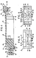
- FIGs 7 and 8 the resulting opto-electronic device is illustrated.
- the opto-electronic equipment of this device is mounted on the plate 70 inserted in the slot and the notches provided for this purpose at the end of the cavity and in the slot 31 of the rear flap 16 folded down and snapped onto the lateral edges 13 and 14 of the housing.
- the stops 32 carried by the flap 16 then ensure the locking in position of the fitted plate 70 in the cavity 20.
- the plate 70 received in its housing 1 carries on its upper face the various components included in the equipment, advantageously mounted in the form of hybrid circuits, not shown. It carries at the end, a transmitting diode 71 and a photodiode 72 whose respective electrical outputs, such as 73 for the diode and 74 for the photodiode, are on the adjacent part of the wafer connected to the hybrid circuits which it carries.
- This diode and the photodiode are thus housed in the separate compartments 23 and 22 provided at the end of the cavity, during the insertion of the plate 70.
- a shield 75 mounted on the wafer 70 covers the diode 71 and extends the compartment 23 which receives the diode 71, towards the inside of the cavity 20, on the wafer 70, by closing it to ensure better insulation of the photodiode.
- This shielding is open at the front, its front part which covers the diode engages in the compartment 23 and comes to double the side and upper walls of the compartment. It is closed at the back; its rear part, on the plate, extends the partition 21, along the corresponding edge of the plate and double the corresponding upper wall of the cavity 20.
- This plate 70 mounted in the housing also carries the aforementioned pins 5, extending in two vertical rows along its longitudinal edges on its underside and connected to the equipment which it carries through it. These pins 5 have their ends protruding from the bottom of the housing.
- the housing 1 receives in its terminal part before the two optical fibers 6 and 7. These fibers, slid into their respective housings, open into the compartments 22 and 23, in line with the diode 71 and the sensitive face of the photodiode 72, respectively. They are locked in the front end part by tightening the nut 8 on a threaded rod 68, with a hexagonal end head 69 locked in the bottom of this part 50.
- Such a method of mounting the optical fibers, for their coupling to the diode and to the photodiode and their retention on the housing, is particularly simple to carry out. This has the advantages of allowing it to be carried out at the places of use of the device and above all that the fibers used are taken from a supply spool or the like and put at the appropriate length when the device is used and therefore depending on its location then chosen in the machine that receives it.
- the box 1 equipped with the opto-electronic equipment board and its fibers respectively coupled to the diode and to the photodiode carried by the board, is in practical use very advantageously mounted as a component on the printed circuit board 2 carrying a operating circuit (not shown).
- the aforementioned screws 3 and 4 ensure its fixing; they are engaged in their housings 57 and 35 provided in the housing (FIG. 4) through this card 2.
- the ends of the pins 5 engage in metallized holes provided for their purpose in the card, and are welded to it.
- the cylindrical pins 59 and 36 mentioned above in relief on the bottom of its front end portion 50 and on the end of the flap and engaged in corresponding passages of the card 2, contribute to the blocking in position of the housing 1 equipped on the card 2 They also prevent the transmission of possible forces exerted on the pins 5 during assembly during the insertion operations of the screws 3 and 4, which could damage their connection with the opto-electronic equipment.
- FIG 9 there is illustrated an opto-electronic circuit mounted on the aforementioned plate 70 of the device shown in Figures 7 and 8.
- This circuit constitutes a circuit for detecting passage of objects, intended in particular to equip an automatic machine mail processing.
- the diode 71 coupled to the optical fiber 6, called the transmitting fiber and the photodiode 72 also coupled to its optical fiber 7 called the receiving fiber.
- the arrow 80 an object to be detected during its passage between the free ends of the fibers.
- the diode 71 is controlled by an oscillator and power stage 81.
- the light emitted by the diode advantageously in the visible range and close to infrared, is thus chopped to differentiate it from ambient light. It is transmitted by the transmitting fiber to the detection point.
- the photodiode 72 is connected to a current / voltage converter 83 followed by an amplifier 84 then a filter 85.
- This filter is connected to a detector 86, itself connected to a comparator 87.
- the signal from the comparator is delivered on an exit 88 through an exit stage 89, with a view to its exploitation.
- the filter 85 eliminates the spurious frequencies contained in the signal from the photodiode.
- the detector 86 detects the variations of this filtered signal during the passage of the object in front of the receiving fiber, it consists of an integrating circuit. In the comparator, the level of the signal received, previously detected, is compared to a fixed or adjustable reference signal, the signal delivered reflects the passage or not of an object in front of the receiving fiber.
- the signal produced by the comparator is transmitted to the use circuit through the output stage.
- the whole of this electronic circuit, associated with the diode 71 and the photodiode 72, is advantageously integrated on the aforementioned plate 70.
- the resulting opto-electronic device equipped with its fibers directly coupled to the diode and to the photodiode is directly pluggable onto any printed circuit board of the operating circuit on which it is therefore treated as a discrete component. This avoids any problem of electrical wiring for its power supply on the one hand and for the exploitation of its detection signals on the other hand.
Landscapes
- Physics & Mathematics (AREA)
- General Physics & Mathematics (AREA)
- Optics & Photonics (AREA)
- Life Sciences & Earth Sciences (AREA)
- General Life Sciences & Earth Sciences (AREA)
- Geophysics (AREA)
- Optical Couplings Of Light Guides (AREA)
Description
- La présente invention est relative aux dispositifs opto-électroniques de détection de passage d'objets, en particulier à ceux destinés à équiper des machines de traitement automatique, telles que notamment des machines de traitement de courrier.
- Les détecteurs optiques sont de manière connue basés soit sur une détection de coupure du faisceau lumineux émis par une source de lumière, lors du passage de l'objet, soit sur une détection du faisceau lumineux issu de la source et renvoyé sur un récepteur lors du passage de l'objet. Dans les détecteurs fonctionnant selon le premier mode cité, la source et le récepteur sont montés face à face d'un côté et de l'autre de la trajectoire de défilement des objets ; dans ceux fonctionnant selon le second mode, la source et le récepteur sont disposés côte à côte, d'un même côté de la trajectoire de défilement des objets.
- Dans de nombreux détecteurs optiques, on associe à la source de lumière des circuits électroniques de commande pour permettre une différenciation entre la lumière émise par la source et la lumière ambiante.
- Ces circuits peuvent comporter un oscillateur à rapport cyclique constant, de fréquence d'oscillation fixe de l'ordre de 20 k Hertz, pilotant un étage de puissance commandant une diode émissive dans le domaine du visible, qui constitue la source de lumière.
- De manière comparable, on associe au récepteur, constitué par une photodiode, des circuits électroniques de traitement du signal reçu en vue de sa détection puis de sa comparaison avec un signal de référence fixe ou variable. Ces derniers circuits peuvent comporter un convertisseur courant/tension du signal issu de la photodiode réceptrice suivi d'un amplificateur de tension, d'un filtre type passe haut du signal amplifié, d'un détecteur type intégrateur assurant la détection de variation du niveau du signal reçu lors du passage de l'objet à détecter puis d'un comparateur et d'un étage de sortie du signal.
- Ces circuits électroniques de commande de la diode et de traitement du signal reçu par la photodiode peuvent avantageusement être regroupés, avec la diode et la photodiode, dans un boîtier équipé de conduits optiques le traversant. Ces conduits optiques sont, lors de la mise de l'équipement en boîtier effectuée en usine, couplés à la diode et à la photodiode respectivement, fixes sur les parois du boîtier qu'ils traversent et mis à une longueur convenable préatablie pour assurer, dans les conditions définies d'utilisation du capteur final résultant, la liaison entre l'équipement interne au boîtier et les points en vis-à-vis ou côte-à-côte de détection de passage d'objets. Un tel capteur ou les capteurs analogues rentrant dans une machine automatisée reçoivent leur alimentation par cable électrique; leur signal électrique de sortie est transmis par câble électrique individuel à un circuit d'exploitation monté sur carte de circuit imprimé, à partir duquel est assurée la commande automatique de la machine. En outre leur emplacement dans une machine automatisée est définitivement conditionné par la longueur donnée aux conduits optiques.
- La présente invention porte sur un dispositif opto-électronique de détection de passage d'objets, pour machine à commande automatisée à partir de ces détections, retenant notamment le principe connu de positionnement du boîtier émetteur-récepteur à distance des points de détection de passage d'objets, par utilisation de conduits optiques, mais d'une part évitant tout problème relatif à l'emplacement du dispositif dans une machine, lié à la longueur qui était donnée aux conduits optiques et d'autre part présentant une conception permettant la suppression des câblages électriques nécessaires au raccordement de chaque dispositif au circuit d'exploitation des signaux de détection et à son alimentation, de manière à constituer un dispositif industriel compact d'utilisation très aisée.
- La présente invention a donc pour objet un dispositif opto-électronique de détection de passage d'objets, à équipement opto- électronique monté dans un boîtier et couplé à des fibres optiques sortant du boîtier, caractérisé par le fait que ledit équipement opto- électronique est porté par une même plaquette et que ledit boîtier est constitué par un corps d'un seul tenant comportant une cavité dans une partie dite principale, constituant le logement de ladite plaquette et équipée de moyens de positionnement et de maintien de ladite plaquette, d'un côté, dit côté avant, une partie terminale avant bordant à l'avant ladite cavité et équipée de passages débouchant dans ladite cavité pour lesdites fibres et de serre-fils pour le maintien de ces fibres et, à l'opposé, formant l'extrémité arrière, un volet rabattable définissant l'accès de ladite plaquette dans la cavité et assurant son blocage.
- Selon une caractéristique de l'invention la ' plaquette porte des broches électriques reliées audit équipement opto-électronique qu'elle porte et dont les extrémités libres débordent sur le fond dudit boîtier, pour un embrochage direct dudit dispositif sur une carte de circuit imprimé.
- Avantageusement, le circuit électronique de l'équipement sera intégré sur la plaquette pour sa miniaturisation tandis que la diode et la photodiode-rentrant dans l'équipement seront montées d'un même côté en bout de la plaquette et raccordées au circuit. Le dispositif résultant sera traité comme un composant discret pour son montage sur une carte de circuit imprimé portant le circuit d'exploitation.
- D'autres caractéristiques et les avantages de la présente invention ressortiront de la description détaillée d'un exemple de réalisation illustré dans le dessin ci-annexé.
- Dans ce dessin:
- - les figures 1 et 2 sont des vues de face et de dessus du dispositif opto-électronique, selon l'invention, représenté monté sur une carte de circuit imprimé,
- - la figure 3 est une vue de dessous du boîtier du dispositif opto-électronique, donnée à échelle agrandie avec arrachements partiels,
- - la figure 4 est une vue en coupe selon la ligne IV-IV de la figure 3,
- - la figure 5 et la figure 6 sont des vues du boîtier, selon les flèches V et VI de la figure 4,
- - les figures 7 et 8 sont deux vues en coupe du dispositif opto-électronique, respectivement selon la ligne VII-Vil de la figure 8 et la ligne VIII-VIII de la figure 7
- - la figure 9 est le schéma synoptique du circuit opto-électronique rentrant dans un dispositif opto-électronique de détection de passage d'objets dans une macnine de traitement automatique de courrier.
- En regard des figures 1 et 2, on voit que le dispositif opto-électronique selon l'invention, illustré tel qu'il sera avantageusement utilisé en pratique, se présente sous la forme d'un boîtier 1 renfermant l'équipement opto-électronique non visible du dispositif et reposant sur une carte de circuit imprimé 2, à laquelle il est fixé par une paire de vis 3 et 4. Cette carte de circuit imprimé 2 constitue une carte de circuit d'exploitation des signaux électriques élaborés par le dispositif opto-électronique qui lui est raccordé par des broches électriques 5 sortant du boîtier 1 et soudées au circuit imprimé de la carte 2, par lesquelles le dispositif opto-électronique reçoit son alimentation et transmet les signaux électriques qu'il élabore.
- Ce boîtier 1 se présente lui-même formé d'une partie principale 10 sensiblement parallélépipédique se prolongeant d'un côté dit côté avant par une partie terminale avant 50. La partie terrminale 50 a sa face supérieure en décrochement sous le niveau de la face supérieure de la partie principale 10 et ses faces latérales en retrait sur celles de la partie principale, les bords inférieurs des parois latérales de ces deux parties 10 et 50 étant au même niveau.
- La partie terminale avant 50 présente une fente horizontale 51, sensiblement au tiers de sa hauteur à partir de sa paroi supérieure. Elle reçoit, au niveau de la fente 51, les extrémités de deux fibres optiques gainées 6 et 7 qui y sont maintenues par un écrou 8 d'un système de serrage de ses deux parties définies de part et d'autre de la fente, formant serre-fil dans cette partie terminale rendue élastiquement déformable.
- Pour la fixation du boîtier 1 sur la carte de circuit imprimé 2, on voit aussi que les vis 3 et 4 sont insérées, pour l'une d'elles 3, dans la partie terminale 50 entre le fond de la fente 51 qu'elle présente et la partie principale 10 et, pour l'autre 4, dans la paroi de la partie principale 10, opposée à la partie terminale avant et dite paroi arrière, présentant à cet effet, extérieurement, une nervure médiane 11 à contour arrondi, sur sa hauteur.
- Dans les figures 3, 4, 5 et 6 on a illustré le boîtier 1 destiné à recevoir l'équipement optoélectronique monté en totalité sur une même plaquette et dont l'ensemble constitue le dispositif opto-électronique.
- Ce boîtier 1 est constitué par un corps d'un seul tenant réalisé en matière plastique et issu directement de moulage.
- La partie principale 10 définit une cavité 20 ouverte sur fond du boîtier 1. Cette partie principale 10 se présente sous la forme d'une plaque 12 bordée latéralement par la partie terminale avant 50 et deux flasques 13 et 14, qui délimitent sur trois côtés la cavité 20. A l'opposé de la partie terminale 50, cette plaque 12 déborde sur les deux flasques 13 et 14 et présente sur sa face interne une rainure 15 qui délimite une portion terminale formant un volet 16 rabattable autour de l'axe X-X (figure 3) pour la constitution, ainsi que schématisé par la flèche F (figure 4), de la quatrième paroi latérale de la cavité 20, à l'extrémité arrière du boîtier 1.
- Ce volet 16 est encliquetable sur les bords adjacents des deux flasques 13 et 14. A cet effet, chacun des deux bords verticaux de ces flasques forme une patte d'accrochage, telle que 17, parallèle au flasque qui la porte mais en retrait sur ce flasque vers l'intérieur de la cavité, qui se termine par un bossage 18 en relief vers l'extérieur de la cavité. En correspondance, le volet 16 présente, sur la face interne de la plaque 12 à laquelle il appartient, deux rebords se terminant par deux bossages arrondis tels que 19 le long de ses deux bords, susceptibles de s'engager derrière les bossages 18 des pattes d'accrochage 17.
- A l'opposé du volet rabattable 16, du côté de la cavité 20, la partie terminale avant 50 forme un décrochement sensiblement à mi-largeur de la cavité, se prolongeant sur une courte distance vers l'intérieur de la cavité en constituant à l'avant ou en bout de la cavité une cloison verticale 21 sensiblement médiane. Cette cloison 21 et les portions des flasques 13 et 14 en regard de cette cloison définissent entre elles deux compartiments verticaux 22 et 23 ayant, sur la partie terminale avant 50, leur fond décalé.
- Avantageusement, le bout ou avant compartimenté de la cavité 20 est de largeur moindre que celle de la cavité elle-même mais supérieure à celle de la partie terminale avant 50. Deux pans inclinés 24 et 34 et 25 et 35 font extérieurement d'un côté et de l'autre ces transitions, tandis qu'à l'intérieur de la cavité 20, au niveau de l'extrémité de la cloison 21 un épaulement tel que 26 sur chacun des flasques rattrappe la transition entre le bout compartimenté de la cavité et la cavité elle-même, donnant une épaisseur accrue aux flasques à ce niveau.
- L'extrémité de la cloison 21 présente à mi-hauteur du boîtier une fente horizontale 27, de faible profondeur. En regard de l'extrémité de cette cloison, chacun des flasques 13 et 14 présente à même niveau une encoche 28 dans l'épaulement qu'il présente, analogue à la fente 27. La fente 27 et l'encoche 28 dans chacun des flasques permettront le maintien d'une plaquette d'équipement opto-électronique à loger dans la cavité 20, par engagement du bord avant et des deux coins avant de cette plaquette dans ces fentes respectives.
- Pour le maintien d'un telle plaquette d'équipement opto-électronique, le volet 16 présente sur sa face intérieure à la cavité, une arête centrale 30. Cette arête à une fente 31 située sensiblement a mi-largeur du volet et analogue à la fente 27 dans la cloison 21, venant, lorsque le volet est rabattu pour fermer la cavité, au même niveau que les fentes 27 et 28. Cette fente 31 recevra le bord arrière de la plaquette d'équipement opto-électronique dont le bord avant a précédemment été engagé dans les fentes 27 et 28, lorsque le volet 16 est rabattu et vient s'encliqueter sur les pattes d'accrochage 17 des flasques.
- Le volet 16 présente aussi, du même côté que l'arête 30, de part et d'autre de celle-ci, deux nervures telles que 32. Ces nervures parallèles aux petits côtés du volet sont de section droite rectangulaire. Elles sont moins hautes que l'arête 30, leur niveau est légèrement supérieur à celui donné par le fond de la fente 31. Lorsque la plaquette d'équipement opto-électronique précitée est insérée dans la cavité 20 et que le volet 16 est rabattu pour fermer l'arrière de la cavité, les nervures 32 viennent en appui contre le bord arrière de la plaquette et constituent alors des butées de maintien en position de la plaquette dans la cavité.
- En outre, on voit que la nervure 11 que présente le boîtier 1 (figures 1 et 2) est formée sur la face du volet 16, opposée à celle portant l'arête 31. Les figures 4 et 6 notamment, laissent apparaître que cette nervure 11 présente un trou borgne 35 ouvert en bout du volet se prolongeant sur l'extrémité du volet dans un ergot cylindrique 36.
- La partie termale 50, forme quant à elle un petit pavé à l'avant de la partie principale 10. Ce pavé, considéré selon la hauteur du boîtier 1 présente un trou 56 le traversant de part en part et un trou borgne 57 débouchant sur le fond du boîtier (figures 3 et 4). Ces deux trous 56 et 57 sont pratiquement alignés, leurs axes étant dans le plan vertical médian de la cloison 21. Alors que le trou débouchant 56 se termine sur le fond du boîtier en une large ouverture 58, de forme hexagonale, pour servir de logement à une tête de tige filetée assurant le blocage en rotation de la tige dans son logement, le trou borgne 57 se prolonge au-delà du niveau du fond du boîtier dans un ergot cylindrique 59.
- Dans la direction donnée par la longueur du boîtier 1, ce pavé présente, outre la fente 51, deux trous 60 et 61 débouchant à l'avant du boîtier et dans la cavité 20, de part et d'autre de la cloison 21 (figures 3 et 5). Ces deux trous 60 et 61 ont leurs axes dans le plan médian de la fente 51 qui les coupe sur une partie de leur longueur. Ces trous 60 et 61 constituent les logements des extrémités des deux fibres optiques 6 et 7 (figures 1 et 2).
- Sur la face inférieure du boîtier 1, ce pavé présente aussi deux empreintes en creux 62 et 63, de part et d'autre des trous 56 et 57 et respectivement au droit des trous 60 et 61 servant de logement aux fibres optiques. Ces empreintes 62 et 63, non ouvertes sur la face avant ou les faces latérales du boîtier, confèrent à la partie terminale avant 50, au niveau des trous 60 et 61, une déformation suffisante pour le blocage des fibres sans risque d'écrasement ou d'endommagement de ces fibres lors du serrage des deux parties définies par la fente 51. Dans la figure 3, en particulier, on voit que l'empreinte 62, correspondant au compartiment 22 le moins profond en bout de la cavité 20, est plus longue que l'empreinte 63.
- Dans les figures 2, 3 et 4, on voit que la face supérieure de ce pavé, au-dessous du niveau donné par la face supérieure du boîtier suit le profil défini par les fonds des deux compartiments, en bout de la cavité, ainsi que schématisé par les deux épaulements 65 et 66 décalés l'un de l'autre qu'elle forme avec la partie supérieure du boîtier.
- Dans les figures 7 et 8 on a illustré le dispositif opto-électronique résultant. L'équipement opto- électronique de ce dispositif est monté sur la plaquette 70 insérée dans la fente et les encoches prévues à cet effet en bout de la cavité et dans la fente 31 du volet arrière 16 rabattu et encliqueté sur les bords latéraux 13 et 14 du boîtier. Les butées 32 portées par le volet 16 assurent alors le blocage en position de la plaquette équipée 70 dans la cavité 20.
- La plaquette 70 reçue dans son boîtier 1 porte sur sa face supérieure les divers composants rentrant dans l'équiqement, avantageusement montés sous forme de circuits hybrides, non représentés. Elle porte en bout, une diode émettrice 71 et une photodiode 72 dont les sorties électriques respectives, telles que 73 pour la diode et 74 pour la photodiode, sont sur la partie adjacente de la plaquette raccordées aux circuits hybrides qu'elle porte. Cette diode et la photodiode viennent ainsi se loger dans les compartiments distincts 23 et 22 prévus en bout de la cavité, lors de l'insertion de la plaquette 70.
- Un blindage 75, monté sur la plaquette 70 recouvre la diode 71 et prolonge le compartiment 23 qui reçoit la diode 71, vers l'intérieur de la cavité 20, sur la plaquette 70, en la fermant pour assurer une meilleure isolation de la photodiode. Ce blindage est ouvert à l'avant, sa partie avant qui recouvre la diode s'engage dans le compartiment 23 et vient doubler les parois latérales et supérieure du compartiment. Il est fermé à l'arrière ; sa partie arrière, sur la plaquette, vient prolonger la cloison 21, longer le bord correspondant de la plaquette et doubler la paroi supérieure correspondante de la cavité 20.
- Cette plaquette 70 montée dans le boîtier porte également les broches 5 précitées, s'étendant en deux rangées verticales le long de ses bords longitudinaux sur sa face inférieure et reliées à l'équipement qu'elle porte à travers elle. Ces broches 5 ont leurs extrémités venant déborder sur le fond du boîtier.
- Outre la plaquette 70 ainsi équipée montée dans la cavité 20, le boîtier 1 reçoit dans sa partie terminale avant les deux fibres optiques 6 et 7. Ces fibres, glissées dans leurs logements respectifs, débouchent dans les compartiments 22 et 23, au droit de la diode 71 et de la face sensible de la photodiode 72, respectivement. Elles sont bloquées dans la partie terminale avant par serrage de l'écrou 8 sur une tige filetée 68, à tête terminale hexagonale 69 bloquée dans le fond de cette partie 50.
- Un tel mode de montage des fibres optiques, pour leur couplage à la diode et à la photodiode et leur maintien sur le boîtier, est particulièrement simple à réaliser. Ceci a pour avantages de permettre qu'il soit réalisé sur les lieux d'utilisation du dispositif et surtout que les fibres utilisées soient prélevées d'une bobine débitrice ou analogue et mises à la longueur adéquate au moment de l'utilisation du dispositif et donc en fonction de son emplacement alors choisi dans la machine qui le reçoit.
- Le boîtier 1 équipé de la plaquette d'équipement opto-électronique et de ses fibres couplées respectivement à la diode et à la photodiode portées par la plaquette, est en utilisation pratique très avantageusement monté comme un composant sur la carte de circuit imprimé 2 portant un circuit d'exploitation (non représenté). Les vis 3 et 4 précitées assurent sa fixation ; elles sont engagées dans leurs logements 57 et 35 prévus dans le boîtier (figure 4) à travers cette carte 2. Lors de ce montage, les extrémités des broches 5 viennent s'engager dans des trous métallisés prévus à leur effet dans la carte, et y sont soudées.
- Les ergots cylindriques 59 et 36, précités en relief sur le fond de sa partie terminale avant 50 et sur l'extrémité du volet et engagés dans des passages correspondants de la carte 2, contribuent au blocage en position du boîtier 1 équipé sur la carte 2. Ils évitent aussi au montage la transmission d'efforts possibles exercés sur les broches 5 lors des opérations d'insertion des vis 3 et 4, qui pourraient endommager leur raccordement avec l'équipement opto- électronique.
- Dans la figure 9, on a illustré un circuit opto- électronique monté sur la plaquette 70 précitée du dispositif représenté dans les figures 7 et 8. Ce circuit constitue un circuit de détection de passages d'objets, destiné en particulier à équiper une machine automatique de traitement de courrier.
- On y a représenté la diode 71 couplée à la fibre optique 6, dite fibre émettrice et la photodiode 72 également couplée à sa fibre optique 7 dite fibre réceptrice. On a schématisé par la flèche 80 un objet à détecter lors de son passage entre les extrémités libres des fibres.
- Dans ce circuit, la diode 71 est commandée par un étage oscillateur et de puissance 81. La lumière émise par la diode, avantageusement dans le domaine du visible et proche de l'infrarouge, est ainsi hachée pour la différencier de la lumière ambiante. Elle est transmise par la fibre émettrice au point de détection.
- La photodiode 72 est reliée à un convertisseur courant/tension 83 suivi d'un amplificateur 84 puis d'un filtre 85. Ce filtre est relié à un détecteur 86, lui-même relié à un comparateur 87. Le signal issu du comparateur est délivré sur une sortie 88 à travers un étage de sortie 89, en vue de son exploitation. Le filtre 85 permet d'éliminer les fréquences parasites contenues dans le signal issu de la photodiode. Le détecteur 86 assure la détection des variations de ce signal filtré lors du passage de l'objet devant la fibre réceptrice, il est constitué par un circuit intégrateur. Dans le comparateur le niveau du signal reçu, précédemment détecté, est comparé à un signal de référence fixe ou ajustable, le signal délivré traduit le passage ou non d'un objet devant la fibre réceptrice. La transmission du signal élaboré par le comparateur vers le circuit d'utilisation est faite à travers l'étage de sortie. L'ensemble de ce circuit électronique, associé à la diode 71 et à la photodiode 72, est avantageusement intégré sur la plaquette 70 précitée. Le dispositif opto-électronique résultant équipé de ses fibres directement couplées à la diode et à la photodiode se trouve directement embrochable sur toute carte de circuit imprimé de circuit d'exploitation sur laquelle il est donc traité comme un composant discret. Ceci évite tout problème de câblage électrique pour son alimentation d'une part et pour l'exploitation de ses signaux de détection d'autre part.
- La présente invention a été décrite en regard de l'exemple de réalisation illustré dans les dessins. Il est évident que l'on peut y apporter des modifications de détail et/ou remplacer certains moyens par d'autres équivalents sans pour autant sortir du cadre de cette invention.
Claims (10)
Applications Claiming Priority (2)
| Application Number | Priority Date | Filing Date | Title |
|---|---|---|---|
| FR8411014A FR2567652B1 (fr) | 1984-07-11 | 1984-07-11 | Dispositif opto-electronique de detection de passage d'objets |
| FR8411014 | 1984-07-11 |
Publications (2)
| Publication Number | Publication Date |
|---|---|
| EP0168023A1 EP0168023A1 (fr) | 1986-01-15 |
| EP0168023B1 true EP0168023B1 (fr) | 1988-11-23 |
Family
ID=9306017
Family Applications (1)
| Application Number | Title | Priority Date | Filing Date |
|---|---|---|---|
| EP85108473A Expired EP0168023B1 (fr) | 1984-07-11 | 1985-07-09 | Dispositif opto-électronique de détection de passage d'objets |
Country Status (5)
| Country | Link |
|---|---|
| US (1) | US4727248A (fr) |
| EP (1) | EP0168023B1 (fr) |
| CA (1) | CA1232648A (fr) |
| DE (1) | DE3566461D1 (fr) |
| FR (1) | FR2567652B1 (fr) |
Families Citing this family (34)
| Publication number | Priority date | Publication date | Assignee | Title |
|---|---|---|---|---|
| DE3637746A1 (de) * | 1986-11-05 | 1988-05-11 | Albatron Gmbh | Opto-elektronischer wandler mit einem anschlussglied fuer einen lichtwellenleiter |
| US5047835A (en) * | 1989-12-26 | 1991-09-10 | At&T Bell Laboratories | Lightwave packaging for pairs of optical devices |
| DE59106807D1 (de) * | 1990-02-17 | 1995-12-07 | Stribel Gmbh | Signalübertragungsleitung. |
| US5005939A (en) * | 1990-03-26 | 1991-04-09 | International Business Machines Corporation | Optoelectronic assembly |
| GB9107657D0 (en) * | 1991-04-11 | 1991-05-29 | Amp Great Britain | Fibre optics connector |
| US5256873A (en) * | 1992-09-03 | 1993-10-26 | Eaton Corporation | Multiple station through beam photoelectric sensor |
| US5337391A (en) * | 1993-05-03 | 1994-08-09 | Motorola, Inc. | Optoelectronic sub-module and method of making same |
| USRE40150E1 (en) | 1994-04-25 | 2008-03-11 | Matsushita Electric Industrial Co., Ltd. | Fiber optic module |
| US5717533A (en) | 1995-01-13 | 1998-02-10 | Methode Electronics Inc. | Removable optoelectronic module |
| US5546281A (en) | 1995-01-13 | 1996-08-13 | Methode Electronics, Inc. | Removable optoelectronic transceiver module with potting box |
| US6220878B1 (en) | 1995-10-04 | 2001-04-24 | Methode Electronics, Inc. | Optoelectronic module with grounding means |
| US5559919A (en) * | 1995-05-25 | 1996-09-24 | Eaton Corporation | Photoelectric optical fiber connector and sensor apparatus |
| US6011254A (en) | 1995-09-21 | 2000-01-04 | Rohm Co., Ltd. | Photoelectric tilt-detecting sensor and method of fabricating the same |
| US5757998A (en) * | 1996-10-02 | 1998-05-26 | International Business Machines Corporation | Multigigabit adaptable transceiver module |
| US6369924B1 (en) | 1998-04-20 | 2002-04-09 | Stratos Lightwave, Inc. | Optical transceiver with enhanced shielding and related methods |
| US6179627B1 (en) | 1998-04-22 | 2001-01-30 | Stratos Lightwave, Inc. | High speed interface converter module |
| US6203333B1 (en) | 1998-04-22 | 2001-03-20 | Stratos Lightwave, Inc. | High speed interface converter module |
| US6031220A (en) * | 1998-06-29 | 2000-02-29 | Berg Technology, Inc. | No touch machine trigger system |
| US6873800B1 (en) | 1999-05-26 | 2005-03-29 | Jds Uniphase Corporation | Hot pluggable optical transceiver in a small form pluggable package |
| US7013088B1 (en) | 1999-05-26 | 2006-03-14 | Jds Uniphase Corporation | Method and apparatus for parallel optical interconnection of fiber optic transmitters, receivers and transceivers |
| US6901221B1 (en) | 1999-05-27 | 2005-05-31 | Jds Uniphase Corporation | Method and apparatus for improved optical elements for vertical PCB fiber optic modules |
| US6213651B1 (en) | 1999-05-26 | 2001-04-10 | E20 Communications, Inc. | Method and apparatus for vertical board construction of fiber optic transmitters, receivers and transceivers |
| US6632030B2 (en) | 1999-05-27 | 2003-10-14 | E20 Communications, Inc. | Light bending optical block for fiber optic modules |
| US20020030872A1 (en) * | 1999-05-27 | 2002-03-14 | Edwin Dair | Method and apparatus for multiboard fiber optic modules and fiber optic module arrays |
| US20010048793A1 (en) * | 1999-05-27 | 2001-12-06 | Edwin Dair | Method and apparatus for multiboard fiber optic modules and fiber optic module arrays |
| US20040069997A1 (en) * | 1999-05-27 | 2004-04-15 | Edwin Dair | Method and apparatus for multiboard fiber optic modules and fiber optic module arrays |
| US6952532B2 (en) * | 1999-05-27 | 2005-10-04 | Jds Uniphase Corporation | Method and apparatus for multiboard fiber optic modules and fiber optic module arrays |
| US7116912B2 (en) * | 1999-05-27 | 2006-10-03 | Jds Uniphase Corporation | Method and apparatus for pluggable fiber optic modules |
| US20010030789A1 (en) * | 1999-05-27 | 2001-10-18 | Wenbin Jiang | Method and apparatus for fiber optic modules |
| US20020033979A1 (en) * | 1999-05-27 | 2002-03-21 | Edwin Dair | Method and apparatus for multiboard fiber optic modules and fiber optic module arrays |
| US7090509B1 (en) | 1999-06-11 | 2006-08-15 | Stratos International, Inc. | Multi-port pluggable transceiver (MPPT) with multiple LC duplex optical receptacles |
| US6220873B1 (en) | 1999-08-10 | 2001-04-24 | Stratos Lightwave, Inc. | Modified contact traces for interface converter |
| US20030147601A1 (en) * | 2002-02-01 | 2003-08-07 | Meir Bartur | Hybrid optical module employing integration of electronic circuitry with active optical devices |
| DE102005007150A1 (de) * | 2005-02-11 | 2006-08-17 | Nordischer Maschinenbau Rud. Baader Gmbh + Co Kg | Vorrichtung und Verfahren zur Erkennung der Ausrichtung/Lage von Produkten, insbesondere von Fischen, auf einem Transportelement |
Family Cites Families (7)
| Publication number | Priority date | Publication date | Assignee | Title |
|---|---|---|---|---|
| US3014161A (en) * | 1959-06-02 | 1961-12-19 | Eldorado Electronics Co | Modular construction |
| US3892962A (en) * | 1972-10-06 | 1975-07-01 | Xerox Corp | Thermal chamber for a developability regulating apparatus |
| US4307934A (en) * | 1978-05-08 | 1981-12-29 | General Dynamics, Pomona Division | Packaged fiber optic modules |
| US4268756A (en) * | 1978-11-13 | 1981-05-19 | Trw Inc. | Optical transceiver |
| GB2044949B (en) * | 1979-03-07 | 1983-04-20 | Vero Electronics Ltd | Terminating connector for a fibre optic cable |
| US4479696A (en) * | 1980-07-07 | 1984-10-30 | Hewlett-Packard Company | Housing for interfacing a semiconductor device with a fiber optic cable |
| US4461537A (en) * | 1981-12-24 | 1984-07-24 | Molex Incorporated | Fiber optic connector assembly |
-
1984
- 1984-07-11 FR FR8411014A patent/FR2567652B1/fr not_active Expired
-
1985
- 1985-06-28 CA CA000485863A patent/CA1232648A/fr not_active Expired
- 1985-07-09 EP EP85108473A patent/EP0168023B1/fr not_active Expired
- 1985-07-09 DE DE8585108473T patent/DE3566461D1/de not_active Expired
-
1987
- 1987-04-24 US US07/042,558 patent/US4727248A/en not_active Expired - Lifetime
Also Published As
| Publication number | Publication date |
|---|---|
| FR2567652A1 (fr) | 1986-01-17 |
| FR2567652B1 (fr) | 1986-11-07 |
| DE3566461D1 (en) | 1988-12-29 |
| CA1232648A (fr) | 1988-02-09 |
| EP0168023A1 (fr) | 1986-01-15 |
| US4727248A (en) | 1988-02-23 |
Similar Documents
| Publication | Publication Date | Title |
|---|---|---|
| EP0168023A1 (fr) | Dispositif opto-électronique de détection de passage d'objets | |
| FR2681711A1 (fr) | Etui portatif pour une carte a memoire electronique. | |
| CA1233564A (fr) | Tete de lecture de marques portees par un document | |
| EP3283329B1 (fr) | Module d'éclairage de l'habitacle d'un véhicule automobile | |
| CH686157A5 (fr) | Detecteur photoelectrique de fumee. | |
| EP2355636B1 (fr) | Ensemble de connexion d'au moins un équipement électronique dans un aéronef | |
| EP0545223B1 (fr) | Bâti d'équipements électroniques, notamment de télécommunications | |
| EP0123595B1 (fr) | Dispositif entrée/sortie pour appareil du genre automate programmable, gamme de tels dispositifs et procédé pour réaliser leur bornier | |
| FR2697951A1 (fr) | Procédé de fixation d'un connecteur amovible sur un connecteur fixe et pièce de fixation. | |
| EP3985631B1 (fr) | Détecteur optique de fumée | |
| EP0434803B1 (fr) | Support de capteur opto-electronique pour compteur de consommation d'energie | |
| EP0911932B1 (fr) | Adaptateur de montage pour appareil électrique à contour non carré | |
| EP0188965A1 (fr) | Bac à cartes électroniques, apte à une connexion électrique par le côté frontal | |
| EP0658078B1 (fr) | Boítier d'habillage électronique à dispositif d'immobilisation de circuits | |
| EP0481878A1 (fr) | Caniveau pour plan(s) de travail destiné à acheminer des câbles vers des appareils posés sur ce(s) plan(s) de travail | |
| EP1033735B1 (fr) | Déclencheur électronique comportant un module long retard amovible associé à une fonction de connexion/déconnexion en tension | |
| EP0921617A1 (fr) | Support pour appareillage à disposer le long d'une goulotte | |
| EP0473482B1 (fr) | Boîte de montage pour appareil électrique | |
| EP0512929B1 (fr) | Rehaussé pour coffret électrique | |
| FR2590028A1 (fr) | Montage d'un shunt dans un boitier de delestage | |
| FR2779281A1 (fr) | Adaptateur pour une unite de commande et unite de commande comportant un tel adaptateur | |
| FR2616034A1 (fr) | Boitier pour circuits electroniques | |
| FR2788547A3 (fr) | Serrure pour coffret hors sol et coffret hors sol de protection d'un dispositif de raccordement equipe d'une telle serrure | |
| EP0298837A1 (fr) | Dispositif de montage d'écran tactile de type optique | |
| CA2123155A1 (fr) | Detecteur de fumee photoelectrique |
Legal Events
| Date | Code | Title | Description |
|---|---|---|---|
| PUAI | Public reference made under article 153(3) epc to a published international application that has entered the european phase |
Free format text: ORIGINAL CODE: 0009012 |
|
| AK | Designated contracting states |
Designated state(s): DE FR GB NL |
|
| 17P | Request for examination filed |
Effective date: 19860715 |
|
| 17Q | First examination report despatched |
Effective date: 19880210 |
|
| GRAA | (expected) grant |
Free format text: ORIGINAL CODE: 0009210 |
|
| AK | Designated contracting states |
Kind code of ref document: B1 Designated state(s): DE FR GB NL |
|
| REF | Corresponds to: |
Ref document number: 3566461 Country of ref document: DE Date of ref document: 19881229 |
|
| GBT | Gb: translation of ep patent filed (gb section 77(6)(a)/1977) | ||
| PLBE | No opposition filed within time limit |
Free format text: ORIGINAL CODE: 0009261 |
|
| STAA | Information on the status of an ep patent application or granted ep patent |
Free format text: STATUS: NO OPPOSITION FILED WITHIN TIME LIMIT |
|
| 26N | No opposition filed | ||
| PGFP | Annual fee paid to national office [announced via postgrant information from national office to epo] |
Ref country code: FR Payment date: 19990615 Year of fee payment: 15 |
|
| PGFP | Annual fee paid to national office [announced via postgrant information from national office to epo] |
Ref country code: NL Payment date: 19990624 Year of fee payment: 15 |
|
| PGFP | Annual fee paid to national office [announced via postgrant information from national office to epo] |
Ref country code: GB Payment date: 19990625 Year of fee payment: 15 |
|
| PGFP | Annual fee paid to national office [announced via postgrant information from national office to epo] |
Ref country code: DE Payment date: 19990628 Year of fee payment: 15 |
|
| PG25 | Lapsed in a contracting state [announced via postgrant information from national office to epo] |
Ref country code: GB Free format text: LAPSE BECAUSE OF NON-PAYMENT OF DUE FEES Effective date: 20000709 |
|
| PG25 | Lapsed in a contracting state [announced via postgrant information from national office to epo] |
Ref country code: NL Free format text: LAPSE BECAUSE OF NON-PAYMENT OF DUE FEES Effective date: 20010201 |
|
| GBPC | Gb: european patent ceased through non-payment of renewal fee |
Effective date: 20000709 |
|
| PG25 | Lapsed in a contracting state [announced via postgrant information from national office to epo] |
Ref country code: FR Free format text: LAPSE BECAUSE OF NON-PAYMENT OF DUE FEES Effective date: 20010330 |
|
| NLV4 | Nl: lapsed or anulled due to non-payment of the annual fee |
Effective date: 20010201 |
|
| REG | Reference to a national code |
Ref country code: FR Ref legal event code: ST |
|
| PG25 | Lapsed in a contracting state [announced via postgrant information from national office to epo] |
Ref country code: DE Free format text: LAPSE BECAUSE OF NON-PAYMENT OF DUE FEES Effective date: 20010501 |