EP0166706B1 - Method for the measurement of capacitances, in particular of low capacitances - Google Patents
Method for the measurement of capacitances, in particular of low capacitances Download PDFInfo
- Publication number
- EP0166706B1 EP0166706B1 EP85850189A EP85850189A EP0166706B1 EP 0166706 B1 EP0166706 B1 EP 0166706B1 EP 85850189 A EP85850189 A EP 85850189A EP 85850189 A EP85850189 A EP 85850189A EP 0166706 B1 EP0166706 B1 EP 0166706B1
- Authority
- EP
- European Patent Office
- Prior art keywords
- capacitance
- measurement
- oscillator
- voltage
- output
- Prior art date
- Legal status (The legal status is an assumption and is not a legal conclusion. Google has not performed a legal analysis and makes no representation as to the accuracy of the status listed.)
- Expired
Links
- 238000005259 measurement Methods 0.000 title claims description 35
- 238000000034 method Methods 0.000 title claims description 25
- 230000000694 effects Effects 0.000 claims description 5
- 230000001419 dependent effect Effects 0.000 claims description 3
- 239000000872 buffer Substances 0.000 description 6
- 230000003321 amplification Effects 0.000 description 2
- 238000010586 diagram Methods 0.000 description 2
- 238000003199 nucleic acid amplification method Methods 0.000 description 2
- 230000001360 synchronised effect Effects 0.000 description 2
- 238000000691 measurement method Methods 0.000 description 1
Images


Classifications
-
- G—PHYSICS
- G01—MEASURING; TESTING
- G01R—MEASURING ELECTRIC VARIABLES; MEASURING MAGNETIC VARIABLES
- G01R27/00—Arrangements for measuring resistance, reactance, impedance, or electric characteristics derived therefrom
- G01R27/02—Measuring real or complex resistance, reactance, impedance, or other two-pole characteristics derived therefrom, e.g. time constant
- G01R27/26—Measuring inductance or capacitance; Measuring quality factor, e.g. by using the resonance method; Measuring loss factor; Measuring dielectric constants ; Measuring impedance or related variables
- G01R27/2605—Measuring capacitance
Definitions
- the present invention is concerned with a method for the measurement of capacitances, in particular of low capacitances, in which method a measurement oscillator is used, whose output frequency is a function of the capacitance to be connected to the input terminals of the circuit determining the frequency of the said oscillator and in which method a known reference capacitance is used, which is connected, being alternatingly exchanged with the capacitance to be measured, to the input terminals of the measurement oscillator while making use of a switching arrangement.
- capacitive detectors In radiosondes, for the measurement of various parameters, in particular of pressure, temperature and humidity, capacitive detectors are used, the magnitude of whose capacitance depends on the parameter being measured.
- the capacitances of these detectors are often relatively low, from a few pF to some dozens of pF, at the maximum about 100 pF.
- the measurement of low capacitances is problematic, e. g., owing to stray capacitances, variations in supply voltage, and other disturbances.
- the said detectors are to some extent individual, so that they have an individual non-linearity and dependence on temperature.
- a reference capacitance which is, alternatingly with the measuring capacitance, connected to the input of the measurement circuit, usually a circuit determining the frequency of a RC-oscillator.
- An objective of the present invention is a further development of the prior-art measurement circuits for low capacitances (0 to 100 pF) so that the measurement circuits become more precise. It is an additional objective of the invention to provide such a measurement circuit in which it is possible to eliminate the effects of switching phenomena.
- a non-essential additional objective of the invention is to provide such a measurement circuit in which the output variable is an appropriately linearized, compensated and scaled DC voltage and to which, if required, a simple temperature compensation may be connected.
- the method in accordance with the invention is mainly characterized in that the capacitance to be measured and the reference capacitance are connected, alternatingly one after the other, to the input terminals of the same said measurement oscillator for the time of an equal number of cycles of the measurement oscillator.
- the frequency of the oscillator is distributed preferably by means of an asynchronous or synchronous divider, and the square wave of the output of the divider is used for controlling analog switches, which exchange the capacitance to be measured with the reference capacitance.
- the output of the divider also controls the data out buffers, one of whose operating voltage terminals has been brought out separately.
- the amplitude of the square wave supplied by the data out buffers can be adjusted and used for linearization, compensation and scaling.
- the temperature dependences of the oscillator affect the lengths of both of the half cycles in the same way, and compensate most of the temperature dependence of the electronics.
- the converting of the pulse ratio to DC voltage, the linearization, compensation and scaling can be accomplished relatively simply by means of data out buffers and RC low pass filter.
- the method in accordance with the invention is carried into effect by making use of an oscillator 10, whereby the capacitance C m to be measured and a precisely known reference capacitance C R are alternatingly connected between the input terminals a and b of the circuit that determines the frequency of the said oscillator 10.
- a parallel capacitance C o is connected, with which the reference capacitance C R and C m are alternatingly connected in parallel.
- a frequency f is obtained as an output variable, which said frequency f is a function of the capacitance C in connected to the inlet terminals: wherein A and B are known constants, and
- the frequency obtained from the output terminal c of the oscillator 10 is passed to the divider 11, which is an asynchronous or synchronous divider, whose division ratio is N. From the divider 11 the output voltage V in is obtained, whose wave form comes out from Fig. 2.
- the capacitance C M to be measured and the reference capacitance C R are alternatingly connected to the same oscillator 10 expressly for an equal number of cycles. This has been accomplished by dividing the frequency f of the oscillator 10 by the divider 11 mentioned above, whose division ratio is denoted with N, and by, by means of the square wave V in of the output of the divider 11, controlling the switches k, and k 2 via an inverter 12.
- the switches k, and k 2 are accomplished, e. g., as analog switches, which are illustrated by the blocks 13a and 13b.
- the switches k 1 and k 2 operate alternatingly so that when the switch k, is closed, the switch k 2 is open, and vice versa.
- the output voltage V in of the divider 11 also controls the data out buffers 15a and 15b, one e (V 1 ) of whose operating voltage terminals has been brought out separately.
- the amplitude of the square wave supplied by the data out buffers 15a and 15b can be adjusted and used for linearization, compensation and scaling, as will come out in more detail in the following in connection with the description of Figures 3, 4 and 5.
- the information on the capacitance to be measured is contained in the half-cycle times T, and T 2 of the output voltage V in of the divider 11, in the way coming out from the following equations (3) to (6).
- the capacitance C m to be measured and the reference capacitance C R are alternatingly connected to the same oscillator circuit 10 for an equal number of cycles, the number of the said cycles being advantageously equal to the division ratio N of the divider 11.
- the switching times T, and T 2 are proportional to the number N of cycles and to the connected capacitance C in .
- the half-cycle lengths T, and T 2 of the square wave V in of the output of the divider 11 are determined by the division ratio N and by the capacitances C M and C R .
- an output voltage illustrating the capacitance C m to be measured is obtained from the output terminals g 1 and/or g 2 of the data out buffer circuit or of the transformer 16, which said output voltage is linearized, temperature-compensated and scaled, making use of the following exemplifying solutions.
- the said transformer 16 may be made of one part, in which case, out of the components 15a and 15b, it includes only the transistors M 1 /M 2 .
- the transformer 16 may be made of two parts, in which case, besides the said transistors M 1 /M 2 , it also includes an inverter 14 and transistors M 3 and M 4 .
- the starting point of the compensation is that, in accordance with the above formulae (4a) and (6a), the output voltages either V 01 or V 01 -V 02 can be compensated in respect of the desired parameter, e. g. the temperature, by arranging the voltage V, as a feedback voltage and the latter as in a suitable way dependent on the parameter to be compensated.
- the desired parameter e. g. the temperature
- the main principle of linearization is that the output voltage is feedback-connected via the terminal e to the transformer 16 as a feedback voltage V 1 .
- the switch 15a/15b acts as a non-linear component, and as a result is obtained non-linear dependence of the output voltage on the pulse ratios X 1 and X 2 defined above (equations (5) and (6)).
- the main principle of scaling is that, by adjusting the voltage V, in the method in accordance with the invention, the range of variation of the output voltage, constituting the output variable dependent on the capacitance C M to be measured (equations 4a and/or 6a), i. e. the scale, can be set at a suitable level.
- the input of an operation amplifier 17, whose amplification is denoted with G, is connected to the output terminals g, and g 2 of the transformer 16 described above.
- the output of the operation amplifier 17 is connected to the output of a resistively feedback-connected operation amplifier 18. From the operation amplifier 18, the output voltage V 2 is obtained.
- B includes the temperature dependences of DC voltage and low frequency as well as the temperature dependences of the delay of.
- the output of the pulse-ratio-DC-voltage transformer 16 is:
Landscapes
- Physics & Mathematics (AREA)
- General Physics & Mathematics (AREA)
- Measurement Of Resistance Or Impedance (AREA)
- Oscillators With Electromechanical Resonators (AREA)
- Stabilization Of Oscillater, Synchronisation, Frequency Synthesizers (AREA)
- Investigating Or Analyzing Materials By The Use Of Electric Means (AREA)
- Testing Or Measuring Of Semiconductors Or The Like (AREA)
- Transmission And Conversion Of Sensor Element Output (AREA)
Description
- The present invention is concerned with a method for the measurement of capacitances, in particular of low capacitances, in which method a measurement oscillator is used, whose output frequency is a function of the capacitance to be connected to the input terminals of the circuit determining the frequency of the said oscillator and in which method a known reference capacitance is used, which is connected, being alternatingly exchanged with the capacitance to be measured, to the input terminals of the measurement oscillator while making use of a switching arrangement.
- One starting point for the present invention has been the prior-art technology that comes out, e. g., from FI-A-54664 and FI-A-57319 (corresponding US-A-4 295 090 and US-A-4 295 091). In the said patents, a method is suggested for the measurement of low capacitances.
- In radiosondes, for the measurement of various parameters, in particular of pressure, temperature and humidity, capacitive detectors are used, the magnitude of whose capacitance depends on the parameter being measured. The capacitances of these detectors are often relatively low, from a few pF to some dozens of pF, at the maximum about 100 pF. The measurement of low capacitances is problematic, e. g., owing to stray capacitances, variations in supply voltage, and other disturbances. Moreover, the said detectors are to some extent individual, so that they have an individual non-linearity and dependence on temperature.
- In particular in telemeter applications, when, e. g., temperature, humidity or pressure is being measured by means of electric or mechano-electric detectors, it is common that, in connection with the measurement electronics, one or several references are provided which are precisely known, so that errors of the measurement circuit and/or of the detector can be eliminated.
- In connection with capacitive detectors, it is known in prior art to use a reference capacitance, which is, alternatingly with the measuring capacitance, connected to the input of the measurement circuit, usually a circuit determining the frequency of a RC-oscillator. By appropriately adjusting the measurement circuit or in some other way, the corresponding output variable of the reference capacitance of the measurement circuit can be brought to the correct level.
- It is known in prior art to use measurement circuits of one reference, in particular bridge connections, in which the measurement is, however, precise only when the electrical value of the reference is close to the value of the detector, e. g., when the bridge is in equilibrium. The more distant the value of the detector becomes from the reference, the larger will also the various errors be, e. g. errors caused by changes in the dynamics of the electronic measurement circuit. An advantage of connections with one reference is the simplicity of the measurement circuit.
- An advantage in measurement arrangements with two or more references is accuracy of the measurement even within wide ranges of measurement, but a drawback is the complexity of the measurement method and of the related computation.
- An objective of the present invention is a further development of the prior-art measurement circuits for low capacitances (0 to 100 pF) so that the measurement circuits become more precise. It is an additional objective of the invention to provide such a measurement circuit in which it is possible to eliminate the effects of switching phenomena.
- A non-essential additional objective of the invention is to provide such a measurement circuit in which the output variable is an appropriately linearized, compensated and scaled DC voltage and to which, if required, a simple temperature compensation may be connected.
- In view of achieving the above objectives and those that will come out in the following, the method in accordance with the invention is mainly characterized in that the capacitance to be measured and the reference capacitance are connected, alternatingly one after the other, to the input terminals of the same said measurement oscillator for the time of an equal number of cycles of the measurement oscillator.
- The frequency of the oscillator is distributed preferably by means of an asynchronous or synchronous divider, and the square wave of the output of the divider is used for controlling analog switches, which exchange the capacitance to be measured with the reference capacitance.
- In a preferred embodiment of the invention, the output of the divider also controls the data out buffers, one of whose operating voltage terminals has been brought out separately. Thereby, the amplitude of the square wave supplied by the data out buffers can be adjusted and used for linearization, compensation and scaling.
- In the invention, by means of a parallel capacitance of the oscillator, a simple temperature compensation can be provided by choosing its temperature coefficient appropriately. The effects of the switching phenomena can be eliminated if the division ratio N of the said divider is sufficiently high, as a rule N > 10.
- The temperature dependences of the oscillator affect the lengths of both of the half cycles in the same way, and compensate most of the temperature dependence of the electronics. The converting of the pulse ratio to DC voltage, the linearization, compensation and scaling can be accomplished relatively simply by means of data out buffers and RC low pass filter.
- In the following, the invention will be described in detail with reference to certain exemplifying embodiments of the invention, illustrated in the figures of the attached drawing, the invention being by no means strictly confined to the details of the said embodiments.
- Figure 1 shows the method in accordance with the invention as a wiring and block diagram.
- Figure 2 shows the wave form of the voltage Vin, which contains the information to be measured.
- Figure 3 shows, as a wiring diagram, linearization of the output voltage, advantageously applicable in connection with the method of the invention.
- Figure 4 shows different wave forms in the wiring system shown in Fig. 3.
- Figure 5 shows the output voltage of the pulse-ratio-DC-voltage transformer as a function of the capacitance to be measured.
- In accordance with Fig. 1, the method in accordance with the invention is carried into effect by making use of an
oscillator 10, whereby the capacitance Cm to be measured and a precisely known reference capacitance CR are alternatingly connected between the input terminals a and b of the circuit that determines the frequency of the saidoscillator 10. Between the inlet terminals of theoscillator 10, a parallel capacitance Co is connected, with which the reference capacitance CR and Cm are alternatingly connected in parallel. From theoscillator 10, a frequency f is obtained as an output variable, which said frequency f is a function of the capacitance Cin connected to the inlet terminals:

- T = a known time constant;
- Cin = CR or CM
- The frequency obtained from the output terminal c of the
oscillator 10 is passed to thedivider 11, which is an asynchronous or synchronous divider, whose division ratio is N. From thedivider 11 the output voltage Vin is obtained, whose wave form comes out from Fig. 2. - It is an essential feature of the invention that the capacitance CM to be measured and the reference capacitance CR are alternatingly connected to the
same oscillator 10 expressly for an equal number of cycles. This has been accomplished by dividing the frequency f of theoscillator 10 by thedivider 11 mentioned above, whose division ratio is denoted with N, and by, by means of the square wave Vin of the output of thedivider 11, controlling the switches k, and k2 via aninverter 12. The switches k, and k2 are accomplished, e. g., as analog switches, which are illustrated by theblocks - In accordance with Fig. 1, the output voltage Vin of the
divider 11 also controls the data outbuffers buffers - The information on the capacitance to be measured is contained in the half-cycle times T, and T2 of the output voltage Vin of the
divider 11, in the way coming out from the following equations (3) to (6).


- As was already stated above, the capacitance Cm to be measured and the reference capacitance CR are alternatingly connected to the
same oscillator circuit 10 for an equal number of cycles, the number of the said cycles being advantageously equal to the division ratio N of thedivider 11. Thus, the switching times T, and T2 are proportional to the number N of cycles and to the connected capacitance Cin. Under these circumstances, the half-cycle lengths T, and T2 of the square wave Vin of the output of thedivider 11 are determined by the division ratio N and by the capacitances CM and CR. The pulse ratios X, and X2 obtained as output, which were defined above in the equations (5) and (6), are proportional to the magnitude of the capacitance CM to be measured, whereas the frequency f is inversely proportional to the said capacitance CM. - According to a preferred embodiment of the invention, an output voltage illustrating the capacitance Cm to be measured is obtained from the output terminals g1 and/or g2 of the data out buffer circuit or of the
transformer 16, which said output voltage is linearized, temperature-compensated and scaled, making use of the following exemplifying solutions. - The said
transformer 16 may be made of one part, in which case, out of thecomponents transformer 16 may be made of two parts, in which case, besides the said transistors M1/M2, it also includes aninverter 14 and transistors M3 and M4. - Output voltage with a one-part transformer:


- Correspondingly, with a two-part transformer:


- By varying the voltage V, to be supplied through the terminal e to the
transformer 16, it is possible to adjust the amplitude of the square wave in accordance with the equation (6a) and, thereby, to provide an advantageous compensation, linearization and scaling of the output voltage. - The starting point of the compensation is that, in accordance with the above formulae (4a) and (6a), the output voltages either V01 or V01-V02 can be compensated in respect of the desired parameter, e. g. the temperature, by arranging the voltage V, as a feedback voltage and the latter as in a suitable way dependent on the parameter to be compensated.
- The main principle of linearization is that the output voltage is feedback-connected via the terminal e to the
transformer 16 as a feedback voltage V1. Thereby, theswitch 15a/15b acts as a non-linear component, and as a result is obtained non-linear dependence of the output voltage on the pulse ratios X1 and X2 defined above (equations (5) and (6)). - The main principle of scaling is that, by adjusting the voltage V,, in the method in accordance with the invention, the range of variation of the output voltage, constituting the output variable dependent on the capacitance CM to be measured (equations 4a and/or 6a), i. e. the scale, can be set at a suitable level.
- In the following, with reference to Figures 3, 4 and 5, a more detailed exemplifying embodiment of the linearization, temperature compensation and scaling of the output voltage used in connection with the method in accordance with the invention will be described.
- In accordance with Fig. 3, the input of an
operation amplifier 17, whose amplification is denoted with G, is connected to the output terminals g, and g2 of thetransformer 16 described above. The output of theoperation amplifier 17 is connected to the output of a resistively feedback-connectedoperation amplifier 18. From theoperation amplifier 18, the output voltage V2 is obtained. - The various wave forms Vin, Vin' and Vin" of the connections illustrated in Fig. are shown in Fig. 4. With different parameters of the wiring system of Fig. 3, the following equations apply, the X, and X2 present in them being defined in the above equations (5) and (6).


- When the equation (15) is examined, it can be noticed that by changing the sign of the amplification G of the
operation amplifier 17, the direction of the curvature of the characteristic curve of the circuit can be changed, and by means of the term k2 (equation 12), the magnitude of the curvature can be adjusted. - In the following, with reference to Fig. 5, the use of a parallel capacitance Co for temperature compensation of the circuit will be described.
- Frequency of a RC oscillator:
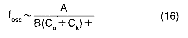
- Temperature has a typical effect on the terms B and . B includes the temperature dependences of DC voltage and low frequency as well as the temperature dependences of the delay of.
- On the basis of (1), (3) and (4), the lengths T, and T2 of the half cycles of the pulse ratio output Vin are:


- In accordance with the above equation (7), the output of the pulse-ratio-DC-
voltage transformer 16 is:
- By appropriate choice of the temperature coefficient of Co (1), it is possible to compensate the temperature dependence of 2T/B partly.
- With reference to Fig. 5, it is noticed that the temperature dependence of 2T/B attempts to alter the angle factor in Fig. 5 at high operating frequencies, whereby the share of T in the time of the half-cycle is important. This can be compensated by means of Co.
- In the following, the patent claims will be given.
Claims (11)
Applications Claiming Priority (2)
| Application Number | Priority Date | Filing Date | Title |
|---|---|---|---|
| FI842192A FI70753C (en) | 1984-05-31 | 1984-05-31 | FOER FARING EQUIPMENT FOR CAPACITORS, SPECIFIC SMAR CAPACITORS. |
| FI842192 | 1984-05-31 |
Publications (2)
| Publication Number | Publication Date |
|---|---|
| EP0166706A1 EP0166706A1 (en) | 1986-01-02 |
| EP0166706B1 true EP0166706B1 (en) | 1989-03-01 |
Family
ID=8519171
Family Applications (1)
| Application Number | Title | Priority Date | Filing Date |
|---|---|---|---|
| EP85850189A Expired EP0166706B1 (en) | 1984-05-31 | 1985-05-30 | Method for the measurement of capacitances, in particular of low capacitances |
Country Status (8)
| Country | Link |
|---|---|
| US (1) | US4775830A (en) |
| EP (1) | EP0166706B1 (en) |
| JP (1) | JPS60262066A (en) |
| CA (1) | CA1268210A (en) |
| DE (1) | DE3568493D1 (en) |
| DK (1) | DK159298C (en) |
| FI (1) | FI70753C (en) |
| NO (1) | NO167830C (en) |
Cited By (1)
| Publication number | Priority date | Publication date | Assignee | Title |
|---|---|---|---|---|
| DE19524387C1 (en) * | 1995-07-04 | 1996-11-07 | Siemens Ag | Capacitance difference measuring circuit for capacitive sensor |
Families Citing this family (14)
| Publication number | Priority date | Publication date | Assignee | Title |
|---|---|---|---|---|
| US4794320A (en) * | 1987-08-10 | 1988-12-27 | Moore Products Co. | Multi-frequency capacitance sensor |
| US5136251A (en) * | 1988-09-23 | 1992-08-04 | John Fluke Mfg. Co., Inc. | Capacitance measurement |
| US5028876A (en) * | 1989-01-30 | 1991-07-02 | Dresser Industries, Inc. | Precision capacitive transducer circuits and methods |
| US5042299A (en) * | 1990-07-23 | 1991-08-27 | Iimorrow, Inc. | Capacitive fluid level sensor |
| US5202640A (en) * | 1991-06-03 | 1993-04-13 | International Business Machines Corporation | Capacitance and leakage test method and apparatus |
| US5148126A (en) * | 1991-12-13 | 1992-09-15 | Sentech Corporation | Capacitance sensor circuit and method for measuring capacitance and small changes in capacitance |
| US5136262A (en) * | 1991-12-13 | 1992-08-04 | Sentech Corporation | Oscillator circuit and method for measuring capacitance and small changes in capacitance |
| US6008660A (en) * | 1996-08-22 | 1999-12-28 | International Business Machines Corporation | Method for developing circuit capacitance measurements corrected for stray capacitance |
| RU2170939C2 (en) * | 1999-08-27 | 2001-07-20 | Ульяновский государственный технический университет | Method of capacitance to frequency conversion |
| EP1439386A4 (en) * | 2001-09-28 | 2005-01-19 | Ngk Spark Plug Co | Oil deterioration sensor |
| US20040246007A1 (en) * | 2003-06-03 | 2004-12-09 | Wolfgang Fallot-Burghardt | Fast, high precision, interference tolerant impedance measurement apparatus |
| JP4713852B2 (en) * | 2003-08-28 | 2011-06-29 | ルネサスエレクトロニクス株式会社 | Frequency generation circuit and communication system using the same |
| DE102008063527A1 (en) * | 2008-12-18 | 2010-07-01 | Micro-Epsilon Messtechnik Gmbh & Co. Kg | Circuit arrangement and method for evaluating a sensor |
| DE102017205908B4 (en) | 2017-04-06 | 2019-04-04 | Marius Czardybon | Evaluation circuit, system and method for evaluating a capacitive or inductive sensor |
Family Cites Families (9)
| Publication number | Priority date | Publication date | Assignee | Title |
|---|---|---|---|---|
| BE567800A (en) * | 1957-10-21 | |||
| AT359599B (en) * | 1977-02-03 | 1980-11-25 | Elin Union Ag | ELECTRONIC CAPACITY MEASURING DEVICE |
| GB2006970B (en) * | 1977-09-23 | 1982-03-31 | Testut Aequitas | Capacitance measuring device |
| FI54664C (en) * | 1977-10-14 | 1979-01-10 | Vaisala Oy | ELECTRONIC EQUIPMENT IN THE SYNERNIZATION FOR TELEMETER MANAGEMENT IN THE SONDER |
| US4295091B1 (en) * | 1978-10-12 | 1995-08-15 | Vaisala Oy | Circuit for measuring low capacitances |
| FR2454083A1 (en) * | 1979-04-09 | 1980-11-07 | Facom | DEVICE FOR MEASURING THE RELATIVE POSITION OF TWO OBJECTS |
| GB2058364B (en) * | 1979-09-01 | 1983-03-23 | Ferranti Ltd | Capacitance measuring apparatus |
| JPS57199914A (en) * | 1981-06-03 | 1982-12-08 | Yokogawa Hokushin Electric Corp | Capacity type converter |
| US4580233A (en) * | 1982-09-22 | 1986-04-01 | Weyerhaeuser Company | Method of measuring moisture content of dielectric materials |
-
1984
- 1984-05-31 FI FI842192A patent/FI70753C/en not_active IP Right Cessation
-
1985
- 1985-05-30 EP EP85850189A patent/EP0166706B1/en not_active Expired
- 1985-05-30 NO NO852170A patent/NO167830C/en unknown
- 1985-05-30 DE DE8585850189T patent/DE3568493D1/en not_active Expired
- 1985-05-30 CA CA000482809A patent/CA1268210A/en not_active Expired - Lifetime
- 1985-05-30 DK DK242385A patent/DK159298C/en not_active IP Right Cessation
- 1985-05-31 JP JP60118679A patent/JPS60262066A/en active Pending
-
1986
- 1986-11-13 US US06/930,580 patent/US4775830A/en not_active Expired - Lifetime
Cited By (1)
| Publication number | Priority date | Publication date | Assignee | Title |
|---|---|---|---|---|
| DE19524387C1 (en) * | 1995-07-04 | 1996-11-07 | Siemens Ag | Capacitance difference measuring circuit for capacitive sensor |
Also Published As
| Publication number | Publication date |
|---|---|
| DK159298C (en) | 1991-02-18 |
| NO167830C (en) | 1991-12-11 |
| DK242385D0 (en) | 1985-05-30 |
| DK159298B (en) | 1990-09-24 |
| JPS60262066A (en) | 1985-12-25 |
| EP0166706A1 (en) | 1986-01-02 |
| FI842192A7 (en) | 1985-12-01 |
| DK242385A (en) | 1985-12-01 |
| NO167830B (en) | 1991-09-02 |
| US4775830A (en) | 1988-10-04 |
| FI70753B (en) | 1986-06-26 |
| DE3568493D1 (en) | 1989-04-06 |
| FI842192A0 (en) | 1984-05-31 |
| NO852170L (en) | 1985-12-02 |
| FI70753C (en) | 1987-01-07 |
| CA1268210A (en) | 1990-04-24 |
Similar Documents
| Publication | Publication Date | Title |
|---|---|---|
| EP0166706A1 (en) | Method for the measurement of capacitances, in particular of low capacitances | |
| US4155257A (en) | Temperature compensated vibrating beam accelerometer | |
| JP2936286B2 (en) | Precision capacitive transducer circuit and method | |
| US4193063A (en) | Differential capacitance measuring circuit | |
| EP0196912A1 (en) | Capacitance bridge | |
| US4169243A (en) | Remote sensing apparatus | |
| US4006430A (en) | Circuit arrangement for converting a bridge unbalance into a frequency variation | |
| US5000048A (en) | Circuit arrangement for temperature compensation of capacitive pressure and differential pressure sensors | |
| EP0693692A2 (en) | Voltage and resistance synthesizer using pulse width modulation | |
| US3510696A (en) | Transducer output correction circuitry | |
| EP0035403A1 (en) | Voltage measuring instrument and preamplifier therefor | |
| EP0303442B1 (en) | Multi-frequency capacitance sensor | |
| US4167697A (en) | Capacitive pick-off circuit | |
| US4597288A (en) | Barometer | |
| SU884587A3 (en) | Device for measuring density of gaseous media | |
| US4634985A (en) | Time-interval signal generating apparatus | |
| NO852169L (en) | PROCEDURE FOR MEASURING CAPACITIES, PARTICULARLY OF LOW VALUE. | |
| CA1262372A (en) | Method for the measurement of capacitances, in particular of low capacitances, wherein two references are used | |
| Zakrzewski | Error propagation in the Interface Electronics for passive sensors | |
| KR810000044B1 (en) | Electric signal transmitter for vibrating-wire sensor | |
| US4001669A (en) | Compensating bridge circuit | |
| SU949539A1 (en) | Conductometric pickup resistance meter | |
| JPH06308176A (en) | Capacitance measuring circuit and lcr metter with the same | |
| SU938256A1 (en) | Device for regulator adjustment | |
| SU1021932A1 (en) | Device for measuring coating thickness |
Legal Events
| Date | Code | Title | Description |
|---|---|---|---|
| PUAI | Public reference made under article 153(3) epc to a published international application that has entered the european phase |
Free format text: ORIGINAL CODE: 0009012 |
|
| AK | Designated contracting states |
Designated state(s): CH DE FR GB IT LI NL SE |
|
| 17P | Request for examination filed |
Effective date: 19860428 |
|
| 17Q | First examination report despatched |
Effective date: 19880502 |
|
| GRAA | (expected) grant |
Free format text: ORIGINAL CODE: 0009210 |
|
| AK | Designated contracting states |
Kind code of ref document: B1 Designated state(s): CH DE FR GB IT LI NL SE |
|
| PG25 | Lapsed in a contracting state [announced via postgrant information from national office to epo] |
Ref country code: IT Free format text: LAPSE BECAUSE OF FAILURE TO SUBMIT A TRANSLATION OF THE DESCRIPTION OR TO PAY THE FEE WITHIN THE PRESCRIBED TIME-LIMIT;WARNING: LAPSES OF ITALIAN PATENTS WITH EFFECTIVE DATE BEFORE 2007 MAY HAVE OCCURRED AT ANY TIME BEFORE 2007. THE CORRECT EFFECTIVE DATE MAY BE DIFFERENT FROM THE ONE RECORDED. Effective date: 19890301 Ref country code: LI Effective date: 19890301 Ref country code: SE Effective date: 19890301 Ref country code: NL Effective date: 19890301 Ref country code: CH Effective date: 19890301 |
|
| REF | Corresponds to: |
Ref document number: 3568493 Country of ref document: DE Date of ref document: 19890406 |
|
| ET | Fr: translation filed | ||
| REG | Reference to a national code |
Ref country code: CH Ref legal event code: PL |
|
| NLV1 | Nl: lapsed or annulled due to failure to fulfill the requirements of art. 29p and 29m of the patents act | ||
| PLBE | No opposition filed within time limit |
Free format text: ORIGINAL CODE: 0009261 |
|
| STAA | Information on the status of an ep patent application or granted ep patent |
Free format text: STATUS: NO OPPOSITION FILED WITHIN TIME LIMIT |
|
| 26N | No opposition filed | ||
| REG | Reference to a national code |
Ref country code: GB Ref legal event code: IF02 |
|
| PGFP | Annual fee paid to national office [announced via postgrant information from national office to epo] |
Ref country code: FR Payment date: 20040428 Year of fee payment: 20 |
|
| PGFP | Annual fee paid to national office [announced via postgrant information from national office to epo] |
Ref country code: GB Payment date: 20040517 Year of fee payment: 20 |
|
| PGFP | Annual fee paid to national office [announced via postgrant information from national office to epo] |
Ref country code: DE Payment date: 20040630 Year of fee payment: 20 |
|
| PG25 | Lapsed in a contracting state [announced via postgrant information from national office to epo] |
Ref country code: GB Free format text: LAPSE BECAUSE OF EXPIRATION OF PROTECTION Effective date: 20050529 |
|
| REG | Reference to a national code |
Ref country code: GB Ref legal event code: PE20 |