EP0166517B1 - Method of depositing a metal on spaced regions of a workpiece - Google Patents
Method of depositing a metal on spaced regions of a workpiece Download PDFInfo
- Publication number
- EP0166517B1 EP0166517B1 EP85303287A EP85303287A EP0166517B1 EP 0166517 B1 EP0166517 B1 EP 0166517B1 EP 85303287 A EP85303287 A EP 85303287A EP 85303287 A EP85303287 A EP 85303287A EP 0166517 B1 EP0166517 B1 EP 0166517B1
- Authority
- EP
- European Patent Office
- Prior art keywords
- copper
- plate
- layer
- anodized
- laser
- Prior art date
- Legal status (The legal status is an assumption and is not a legal conclusion. Google has not performed a legal analysis and makes no representation as to the accuracy of the status listed.)
- Expired
Links
- 238000000034 method Methods 0.000 title claims abstract description 40
- 238000000151 deposition Methods 0.000 title claims abstract description 24
- 229910052751 metal Inorganic materials 0.000 title claims abstract description 21
- 239000002184 metal Substances 0.000 title claims abstract description 21
- RYGMFSIKBFXOCR-UHFFFAOYSA-N Copper Chemical compound [Cu] RYGMFSIKBFXOCR-UHFFFAOYSA-N 0.000 claims abstract description 38
- 229910052802 copper Inorganic materials 0.000 claims abstract description 38
- 239000010949 copper Substances 0.000 claims abstract description 38
- 229910052782 aluminium Inorganic materials 0.000 claims abstract description 22
- XAGFODPZIPBFFR-UHFFFAOYSA-N aluminium Chemical compound [Al] XAGFODPZIPBFFR-UHFFFAOYSA-N 0.000 claims abstract description 22
- 238000000576 coating method Methods 0.000 claims abstract description 13
- 239000011248 coating agent Substances 0.000 claims abstract description 12
- 239000004411 aluminium Substances 0.000 claims abstract description 11
- 230000001678 irradiating effect Effects 0.000 claims abstract description 4
- 239000010410 layer Substances 0.000 claims description 36
- 230000008021 deposition Effects 0.000 claims description 16
- 239000003792 electrolyte Substances 0.000 claims description 16
- QAOWNCQODCNURD-UHFFFAOYSA-N Sulfuric acid Chemical compound OS(O)(=O)=O QAOWNCQODCNURD-UHFFFAOYSA-N 0.000 claims description 10
- 239000000758 substrate Substances 0.000 claims description 10
- PNEYBMLMFCGWSK-UHFFFAOYSA-N Alumina Chemical compound [O-2].[O-2].[O-2].[Al+3].[Al+3] PNEYBMLMFCGWSK-UHFFFAOYSA-N 0.000 claims description 9
- 239000002344 surface layer Substances 0.000 claims description 8
- 238000007654 immersion Methods 0.000 claims description 6
- 239000011148 porous material Substances 0.000 claims description 5
- ARUVKPQLZAKDPS-UHFFFAOYSA-L copper(II) sulfate Chemical compound [Cu+2].[O-][S+2]([O-])([O-])[O-] ARUVKPQLZAKDPS-UHFFFAOYSA-L 0.000 claims description 4
- 239000001117 sulphuric acid Substances 0.000 claims description 3
- 235000011149 sulphuric acid Nutrition 0.000 claims description 3
- 239000011261 inert gas Substances 0.000 claims 1
- JPVYNHNXODAKFH-UHFFFAOYSA-N Cu2+ Chemical compound [Cu+2] JPVYNHNXODAKFH-UHFFFAOYSA-N 0.000 abstract description 3
- 229910001431 copper ion Inorganic materials 0.000 abstract description 3
- 238000004519 manufacturing process Methods 0.000 abstract description 3
- CURLTUGMZLYLDI-UHFFFAOYSA-N Carbon dioxide Chemical compound O=C=O CURLTUGMZLYLDI-UHFFFAOYSA-N 0.000 description 16
- 239000001569 carbon dioxide Substances 0.000 description 8
- 229910002092 carbon dioxide Inorganic materials 0.000 description 8
- 239000000463 material Substances 0.000 description 8
- 230000005855 radiation Effects 0.000 description 7
- 230000015572 biosynthetic process Effects 0.000 description 6
- 239000000975 dye Substances 0.000 description 6
- 206010034972 Photosensitivity reaction Diseases 0.000 description 4
- XKRFYHLGVUSROY-UHFFFAOYSA-N argon Substances [Ar] XKRFYHLGVUSROY-UHFFFAOYSA-N 0.000 description 4
- 229910052786 argon Inorganic materials 0.000 description 4
- -1 argon ion Chemical class 0.000 description 4
- 238000002474 experimental method Methods 0.000 description 3
- 238000005286 illumination Methods 0.000 description 3
- 238000003384 imaging method Methods 0.000 description 3
- 230000003287 optical effect Effects 0.000 description 3
- TWNQGVIAIRXVLR-UHFFFAOYSA-N oxo(oxoalumanyloxy)alumane Chemical compound O=[Al]O[Al]=O TWNQGVIAIRXVLR-UHFFFAOYSA-N 0.000 description 3
- 230000001105 regulatory effect Effects 0.000 description 3
- 238000010521 absorption reaction Methods 0.000 description 2
- 238000002048 anodisation reaction Methods 0.000 description 2
- 238000007743 anodising Methods 0.000 description 2
- 238000006243 chemical reaction Methods 0.000 description 2
- 230000003750 conditioning effect Effects 0.000 description 2
- 239000008151 electrolyte solution Substances 0.000 description 2
- 229910044991 metal oxide Inorganic materials 0.000 description 2
- 239000000203 mixture Substances 0.000 description 2
- 238000012360 testing method Methods 0.000 description 2
- MQRWBMAEBQOWAF-UHFFFAOYSA-N acetic acid;nickel Chemical compound [Ni].CC(O)=O.CC(O)=O MQRWBMAEBQOWAF-UHFFFAOYSA-N 0.000 description 1
- 230000002411 adverse Effects 0.000 description 1
- 230000005540 biological transmission Effects 0.000 description 1
- 230000006835 compression Effects 0.000 description 1
- 238000007906 compression Methods 0.000 description 1
- 230000001143 conditioned effect Effects 0.000 description 1
- 238000007796 conventional method Methods 0.000 description 1
- 150000001879 copper Chemical class 0.000 description 1
- 229910000365 copper sulfate Inorganic materials 0.000 description 1
- 238000011161 development Methods 0.000 description 1
- 230000000694 effects Effects 0.000 description 1
- 238000009713 electroplating Methods 0.000 description 1
- 239000012530 fluid Substances 0.000 description 1
- 238000010438 heat treatment Methods 0.000 description 1
- 150000002500 ions Chemical class 0.000 description 1
- QSHDDOUJBYECFT-UHFFFAOYSA-N mercury Chemical compound [Hg] QSHDDOUJBYECFT-UHFFFAOYSA-N 0.000 description 1
- 229910052753 mercury Inorganic materials 0.000 description 1
- 229910001507 metal halide Inorganic materials 0.000 description 1
- 150000005309 metal halides Chemical class 0.000 description 1
- 150000004706 metal oxides Chemical class 0.000 description 1
- 229940078494 nickel acetate Drugs 0.000 description 1
- 238000007747 plating Methods 0.000 description 1
- 238000002207 thermal evaporation Methods 0.000 description 1
- 230000000007 visual effect Effects 0.000 description 1
Images


Classifications
-
- B—PERFORMING OPERATIONS; TRANSPORTING
- B41—PRINTING; LINING MACHINES; TYPEWRITERS; STAMPS
- B41C—PROCESSES FOR THE MANUFACTURE OR REPRODUCTION OF PRINTING SURFACES
- B41C1/00—Forme preparation
- B41C1/10—Forme preparation for lithographic printing; Master sheets for transferring a lithographic image to the forme
- B41C1/1008—Forme preparation for lithographic printing; Master sheets for transferring a lithographic image to the forme by removal or destruction of lithographic material on the lithographic support, e.g. by laser or spark ablation; by the use of materials rendered soluble or insoluble by heat exposure, e.g. by heat produced from a light to heat transforming system; by on-the-press exposure or on-the-press development, e.g. by the fountain of photolithographic materials
- B41C1/1033—Forme preparation for lithographic printing; Master sheets for transferring a lithographic image to the forme by removal or destruction of lithographic material on the lithographic support, e.g. by laser or spark ablation; by the use of materials rendered soluble or insoluble by heat exposure, e.g. by heat produced from a light to heat transforming system; by on-the-press exposure or on-the-press development, e.g. by the fountain of photolithographic materials by laser or spark ablation
-
- B—PERFORMING OPERATIONS; TRANSPORTING
- B41—PRINTING; LINING MACHINES; TYPEWRITERS; STAMPS
- B41N—PRINTING PLATES OR FOILS; MATERIALS FOR SURFACES USED IN PRINTING MACHINES FOR PRINTING, INKING, DAMPING, OR THE LIKE; PREPARING SUCH SURFACES FOR USE AND CONSERVING THEM
- B41N3/00—Preparing for use and conserving printing surfaces
- B41N3/08—Damping; Neutralising or similar differentiation treatments for lithographic printing formes; Gumming or finishing solutions, fountain solutions, correction or deletion fluids, or on-press development
-
- C—CHEMISTRY; METALLURGY
- C25—ELECTROLYTIC OR ELECTROPHORETIC PROCESSES; APPARATUS THEREFOR
- C25D—PROCESSES FOR THE ELECTROLYTIC OR ELECTROPHORETIC PRODUCTION OF COATINGS; ELECTROFORMING; APPARATUS THEREFOR
- C25D11/00—Electrolytic coating by surface reaction, i.e. forming conversion layers
- C25D11/005—Apparatus specially adapted for electrolytic conversion coating
-
- C—CHEMISTRY; METALLURGY
- C25—ELECTROLYTIC OR ELECTROPHORETIC PROCESSES; APPARATUS THEREFOR
- C25D—PROCESSES FOR THE ELECTROLYTIC OR ELECTROPHORETIC PRODUCTION OF COATINGS; ELECTROFORMING; APPARATUS THEREFOR
- C25D5/00—Electroplating characterised by the process; Pretreatment or after-treatment of workpieces
- C25D5/02—Electroplating of selected surface areas
- C25D5/024—Electroplating of selected surface areas using locally applied electromagnetic radiation, e.g. lasers
-
- C—CHEMISTRY; METALLURGY
- C25—ELECTROLYTIC OR ELECTROPHORETIC PROCESSES; APPARATUS THEREFOR
- C25D—PROCESSES FOR THE ELECTROLYTIC OR ELECTROPHORETIC PRODUCTION OF COATINGS; ELECTROFORMING; APPARATUS THEREFOR
- C25D5/00—Electroplating characterised by the process; Pretreatment or after-treatment of workpieces
- C25D5/34—Pretreatment of metallic surfaces to be electroplated
- C25D5/42—Pretreatment of metallic surfaces to be electroplated of light metals
- C25D5/44—Aluminium
-
- Y—GENERAL TAGGING OF NEW TECHNOLOGICAL DEVELOPMENTS; GENERAL TAGGING OF CROSS-SECTIONAL TECHNOLOGIES SPANNING OVER SEVERAL SECTIONS OF THE IPC; TECHNICAL SUBJECTS COVERED BY FORMER USPC CROSS-REFERENCE ART COLLECTIONS [XRACs] AND DIGESTS
- Y10—TECHNICAL SUBJECTS COVERED BY FORMER USPC
- Y10S—TECHNICAL SUBJECTS COVERED BY FORMER USPC CROSS-REFERENCE ART COLLECTIONS [XRACs] AND DIGESTS
- Y10S204/00—Chemistry: electrical and wave energy
- Y10S204/07—Current distribution within the bath
-
- Y—GENERAL TAGGING OF NEW TECHNOLOGICAL DEVELOPMENTS; GENERAL TAGGING OF CROSS-SECTIONAL TECHNOLOGIES SPANNING OVER SEVERAL SECTIONS OF THE IPC; TECHNICAL SUBJECTS COVERED BY FORMER USPC CROSS-REFERENCE ART COLLECTIONS [XRACs] AND DIGESTS
- Y10—TECHNICAL SUBJECTS COVERED BY FORMER USPC
- Y10S—TECHNICAL SUBJECTS COVERED BY FORMER USPC CROSS-REFERENCE ART COLLECTIONS [XRACs] AND DIGESTS
- Y10S205/00—Electrolysis: processes, compositions used therein, and methods of preparing the compositions
- Y10S205/918—Use of wave energy or electrical discharge during pretreatment of substrate or post-treatment of coating
Definitions
- This invention relates in general to the deposition of a metal by electrolytic means on selected regions of a workpiece for pattern generation on anodized aluminium lithographic printing plates by the treatment of selected regions of the plates followed by the electrolytic deposition of metal on these regions.
- Conventional lithographic recording techniques consist of several steps which include forming a 1:1 negative of a paste up, or original copy, to be printed, developing the negative, vacuum contacting the negative onto a photosensitized plate, and directing light from a mercury vapour or metal halide lamp through the entire negative simultaneously, thereby exposing the photosensitive coated, plate.
- the plate must then be developed, for example by removal of the unexposed photosensitive material.
- This method requires at least several minutes to complete and is both labour- and materials-intensive.
- the resulting plates may lack the durability need to print large numbers of copies, and/or lack the shelf life needed to permit their re-use several months following an initial print run.
- a laser can image graphics or text onto either film or directly onto photosensitized plates.
- the laser beam can be vector-or raster-scanned over the film, its trajectory being controlled and its amplitude being modulated by a computer.
- Such film exposure requires only a low power laser.
- the resultant negative must subsequently be used in a manner similar to that of conventional techniques to expose a photosensitized plate.
- the computer-controlled beam can image graphics or text directly onto a photosensitized plate surface.
- Direct laser plate imaging systems may include a low power laser scanner, such as a HeNe laser, which reads and electronically stores printed matter from the paste up, and a high power ultraviolet laser writing unit which exposes an ultraviolet photosensitive coating on a lithographic plate in accordance with information stored in a computer.
- a low power laser scanner such as a HeNe laser
- a high power ultraviolet laser writing unit which exposes an ultraviolet photosensitive coating on a lithographic plate in accordance with information stored in a computer.
- this known method is characterised in that the electrically conductive substrate is an aluminium plate which is anodized to form the electrically insulative layer and the irradiation is effected by rapidly scanning the layer with the laser beam which is pulsed to fracture or remove the anodized layer in a multiplicity of dot-like regions.
- the method is particularly applicable to the production of printing plates the print features of which are durable and capable of long print runs and have a long shelf life.
- the method may also be more rapid, labour saving, and less material intensive than existing methods.
- an aluminium plate having a porous, dye-filled anodized surface layer of aluminium oxide is irradiated in air by a laser such as a beam- modulated, continuous wave carbon dioxide or Nd:YAG laser.
- the focused laser beam shrinks the upper portion of the anodized layer. This exposes the underlying aluminium through small cracks in areas of the plate to which laser energy is applied.
- the laser beam and/or the plate is steered to irradiate areas corresponding to the printing features to be produced.
- the plate is then immersed in an electrolytic bath such as copper sulphate and sulphuric acid with the plate negatively biased, and a layer of copper of desired thickness is electrolytically deposited on the exposed aluminium to produce copper printing features.
- an anodized aluminium plate is immersed in an electrolytic bath such as copper sulphate and sulphuric acid, and the plate, while negatively biased, is irradiated by a suitable laser.
- the laser beam is steered in a predetermined pattern and copper is electrolytically deposited in the areas whose anodized layer has been fractured by the laser to expose underlying aluminium.
- deposition of printing features in a specific area starts to occur immediately following laser irradiation, and since the irradiated plate is not in contact with air, there is no risk of the formation on the exposed aluminium areas of an electrically resistive film, such as a metal oxide, which could modify deposition of the copper printing features.
- This embodiment is, however, limited to laser wavelengths which can be transmitted through the electrolytic solution. Also, because the laser beam diffracts in passing through the electrolyte, the resolution of copper features deposited in this manner may be lower than obtainable in the earlier-described method wherein the plate is irradiated outside of, and prior to its immersion into, the electrolytic bath.
- appropriately coloured dyes are embedded in the pores of the anodized layer of the plate to enhance the absorption of the laser beam and thereby increase its efficiency in fracturing the surface.
- the pulsing of the laser beam as by mechanical chopping, produces dots rather than continuous lines as printing features, which enables the printing of half tones.
- the copper printing features on an anodized aluminium background produced according to the above described methods provide an excellent combination for high quality, wear resistant printing plates with long shelf life.
- these features are fabricated so as to be indented or recessed below the surface of the surrounding anodized layer by, for example, regulating laser power and steering rate such that a portion of the surface layer is shrunk or removed and regulating electrolytic deposition such that the copper layer deposited does not completely fill the recess.
- the resulting recessed features will more readily retain ink and suffer less wear during printing, thereby providing even better print quality and longer plate life.
- the conditioning laser is an infrared laser and the deposited metal is copper.
- This embodiment can be used to form printed features, graphics and text, on a printing plate used, for example, in offset planographic printing.
- Fig. 1 shows in schematic form a preferred set of components and the manner in which they are utilized to produce metal coatings on selected areas of a metal substrate according to one form of the invention.
- a plate 20 is prepared by coating an aluminum base 24 with a film of aluminum oxide 28 about 5 um to 25 pm thick using a standard anodizing process such as sulfuric acid anodization. During the latter stages of this process a dye of selected color such as a black or gray dye is embedded in the pores of the aluminum oxide coating and the dye is sealed as by treating the surface of the anodized layer with nickel acetate.
- a standard anodizing process such as sulfuric acid anodization.
- the plate 20 is conditioned by exposure to the beam 32 of a laser 36 which may be selected from a wide variety of commercially available units and may emit any wavelength from the ultraviolet to the infrared.
- the laser currently preferred from the standpoint of performance and economy is either a Nd:YAG laser or a carbon dioxide laser emitting in the infrared at, respectively, 1.06 um and 10.6 pm.
- Continuous wave 100 W (watt) Nd:YAG and 400 W carbon dioxide lasers are readily available, whereas the strongest available continuous wave argon ion visible laser is limited to about 20 W.
- the additional power of the infrared lasers allows a faster writing speed, or a shorter illumination time, of the laser beam 52 on the anodized surface 28 than would be attainable with argon ion visible lasers or the ultraviolet lasers typically used to expose photosensitive materials in conventional platemaking processes.
- the formation, or writing, of text or graphics features on this anodized surface 28 is performed by focusing the output beam 40 of the laser 36 by means of a lens 44 through an acousto optic modulator 48 in'orderto amplitude modulate the radiation and convert continuous emission of the beam 40 to a pulsed beam 52.
- pulses of radiation are passed through and focused by a second lens 56, reflect from a mirrored surface such as a galvanometrically-controlled mirror 64 of an optical scanner 60, and are directed onto the anodized surface 28.
- the optical scanner 60 sweeps the pulses of radiation across the anodized surface 28.
- the optical scanner 60 may comprise a rapidly rotating polygon (not shown) containing a number of mirrored facets instead of the galvanometrically-controlled mirror 64.
- the pulsed beam 56 can be positioned at any point on the stationary anodized surface 28. This configuration lends itself to vector scanning of the printing plate 20 by the laser beam 32.
- the printing plate 20 is mounted on a drum and rotated in a direction perpendicular to the scanning direction of the beam 52.
- the anodized surface 28 would be raster-scanned.
- the pulsed beam will form a series of resolvable dots on the anodized surface 28.
- the minimum dot size which can be printed is determined by the diffraction limited focus of th.e laser beam 52.
- the diameter of the spot will be proportional to the lasing wavelength. Consequently, the minimum spot size of the carbon-dioxide laser emission would be expected to be about twenty times as large as that of the argon ion laser, and about ten times that of the Nd:YAG laser.
- the widths of the deposited copper lines have not shown this trend.
- the lateral extent of the laser induced cracks which form in the anodized surface depend not only on the lasing wavelength, beam width, and lens focal length, but also on the laser power, the beam scanning speed, the radiation absorption depth in the anodized layer, and the electrolytic bath parameters and plate immersion time. These additional parameters influence the stress concentration built up in the anodized layer, and, consequently, the extent of fractures induced by the laser beam in this surface film and the lateral distance from the crack that the copper will coat.
- a carbon dioxide laser Model No.
- the plate 20 after exposure to the scanning laser beam 36, is immersed in an electrolytic tank 68 containing a mixture of an electrolyte 72 composed of copper sulfate (C U S0 4 ) and sulfuric acid (H 2 SO 4 ).
- the copper will fill the cracks in the anodized layer 28 and then continue to deposit over the surface of the anodized layer away from the cracks.
- the extent of this coating from the cracks is determined by the composition of the electrolytic bath in the electrolytic tank 68, the current passing through the electrolyte 72 and the time the plate 20 is immersed in this electrolyte 72.
- the method of laser-induced selective plating of the invention therefore consists of two distinct processes: laser irradiation of specific areas on a surface, followed by electrolytic deposition of a metal on those areas.
- Fig. 2 shows two configurations for practicing the method. In the form illustrated in Fig. 2a an unexposed cathode 78 to be plated is submerged within electrolyte 80 in a tank 82 and a laser beam is focused by a lens 86 and is directed through a hole 90 in an anode 92 onto the areas of the cathode 78 to be plated.
- the beam 82 may be scanned over predetermined portions of the cathode 78, in addition to which the cathode 78 may be moved to expose selected areas to the laser beam 82). Electrolytic plating occurs immediately after irradiation by the laser beam 84 and without the cathode being exposed to atmospheric conditions between these two processes.
- a plate 96 is positioned outside an electrolytic tank 98 and irradiated by a laser beam 102 focused onto the plate 96 by a lens 106. Subsequently, the plate 96 is immersed in the electrolytic bath 104 and metal is electrolytically deposited on the laser exposed surface area as current passes through electrolyte 104 between an anode 110 and the plate 94.
- the configuration shown in Fig. 2a has the advantage that the plate 78 is not exposed to any environment other than the electrolytic bath 80 after laser irradiation of its surface. Such exposure to, say, the atmosphere, as in the configuration shown in Fig. 2b, could result in formation of a metallic oxide film on the bare metal surface underlying the laser-induced cracks in the anodized surface layer. Formation of a sufficiently thick electrically insulating oxide layer would influence the electrolytic reaction and adversely affect deposition of the metal coating in the laser irradiated areas.
- the laser beam 84 in passing through the electrolyte 80 and heating this fluid may suffer diffraction, an effect which is maximized by thermally induced changes in the refractive index of the electrolyte 80 at the focus of the beam 84 on the surface of the plate 78.
- Such diffraction will defocus the beam and increase the image size, thereby reducing the resolution of metallic features electrolytically deposited on the surface of the plate 78.
- Another disadvantage of irradiating the plate 78 while it is submerged in the electrolyte is that only lasers emitting at wavelengths which are transmitted by the electrolyte can be used. Separating the processes, as shown in Fig.
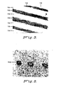
- a series of copper lines 114 electrolytically deposited on an anodized surface subsequent to irradiation in air of the areas corresponding to these lines by a carbon dioxide laser beam is shown in the photomicrograph of Fig. 3.
- the copper lines 114 are about 33 pm wide and the uncoated anodized strips 118 between the lines are about 21 ⁇ m wide.
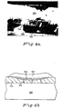
- the structure of a deposited feature is illustrated by a photomicrograph of a cross-section of a copper line (Fig. 4a) and by the sketch of the cross-section set forth as Fig. 4b. These show a laser-modified zone 122 in the anodized layer 126 and a copper deposit 130 about 14 pm thick overlying the laser-modified zone 122.
- zone 122 With respect to the subsequent copper deposition is not yet understood, but some removal or shrinkage of the anodized layer 126 appears to occur.
- Laser-induced cracks 134 in the zone 122 and in the underlying unmodified anodized layer 126 form an electrical path connecting the aluminum base 138 to copper ions in the electrolytic bath to allow the electrolytic deposition of copper first in the cracks 134 and then over the laser-modified zone in the anodized layer 126.
- the thickness of the deposited copper lines varies with the characteristics of the electrolytic bath, the current passing through the electrolyte, and the amount of time the plate is immersed in the electrolyte. Uniform 2 um thick copper deposition has been obtained across across lines 120 pm wide.
- Fig. 5 is a photomicrograph showing the results of electrolytically depositing copper on laser irradiated spots formed by mechanically chopping a continuous beam from an argon ion laser operated at a wavelength of 488 nanometers and projecting the focused radiation pulses on different spatial locations of an anodized aluminum surface.
- copper deposits 142 having a diameter of about 60 pm were produced, but only on the irradiated spots. This indicates that the cracks which are formed by the laser in the anodized layer do not migrate significantly outside the region of illumination.
- test plates were fabricated of aluminum a!loy 5052 and were anodized by Light Metal Platers, Inc. of Waltham, Massachusetts using a standard sulfuric acid anodizing process.
- the thickness of the anodized layers ranged from about 7 to 25 pm. Best results were obtained on black-dyed plates having an anodization thickness of about 7 um irradiated by the carbon dioxide laser. With a laser output power of 4 W, a 35 micrometer wide line was exposed at a laser beam scanning speed of approximately 15 centimeters per second.
- This line consisted of a zone extending about half way down the anodized layer into the recess formed by the apparent shrinkage and/or removal of this layer (the "shrinkage” possibly due to thermal evaporation of the dye within the pores and compression of the anodized material in this region).
- a number of thin (less than 1 pm) cracks were formed through the anodized layer. These cracks followed the direction of the scanning laser beam and extended down to the base aluminum. Such fracturing is thought to be caused by laser-induced thermal gradients in the aluminum oxide layer which causes mechanical stressing of this material.
- anodized samples were irradiated by the laser in air at atmospheric conditions, they were (within 60 minutes) immersed in an electrolytic solution containing 0.5 M C U S0 4 and 2 M H 2 S0 4 . With a negative voltage of 0.5 V on the aluminum base material approximately 100 mA of current was drawn. Copper deposits having a thickness of several um were achieved after about 30 seconds of electrolytic reaction.
Landscapes
- Chemical & Material Sciences (AREA)
- Engineering & Computer Science (AREA)
- Metallurgy (AREA)
- Optics & Photonics (AREA)
- Organic Chemistry (AREA)
- Physics & Mathematics (AREA)
- Chemical Kinetics & Catalysis (AREA)
- Electrochemistry (AREA)
- Materials Engineering (AREA)
- Manufacturing & Machinery (AREA)
- Thermal Sciences (AREA)
- Electromagnetism (AREA)
- Printing Plates And Materials Therefor (AREA)
- Electroplating Methods And Accessories (AREA)
- Manufacture Or Reproduction Of Printing Formes (AREA)
- Photosensitive Polymer And Photoresist Processing (AREA)
- Internal Circuitry In Semiconductor Integrated Circuit Devices (AREA)
Abstract
Description
- This invention relates in general to the deposition of a metal by electrolytic means on selected regions of a workpiece for pattern generation on anodized aluminium lithographic printing plates by the treatment of selected regions of the plates followed by the electrolytic deposition of metal on these regions.
- Recording information by the generation, or "writing", of precise patterns on lithographic printing plates is an important step in the production of newspapers and other printed materials. Thus there is considerable interest in developing techniques which reduce the time, material, and labour required to record lithographic printing plate patterns that are wear-resistant and have a long shelf life.
- Conventional lithographic recording techniques consist of several steps which include forming a 1:1 negative of a paste up, or original copy, to be printed, developing the negative, vacuum contacting the negative onto a photosensitized plate, and directing light from a mercury vapour or metal halide lamp through the entire negative simultaneously, thereby exposing the photosensitive coated, plate. The plate must then be developed, for example by removal of the unexposed photosensitive material. This method requires at least several minutes to complete and is both labour- and materials-intensive. Moreover, the resulting plates may lack the durability need to print large numbers of copies, and/or lack the shelf life needed to permit their re-use several months following an initial print run.
- In certain parts of the printing industry laser imaging techniques have now been found preferable to conventional platemaking processes. A laser can image graphics or text onto either film or directly onto photosensitized plates. When used to expose film the laser beam can be vector-or raster-scanned over the film, its trajectory being controlled and its amplitude being modulated by a computer. Such film exposure requires only a low power laser. However, the resultant negative must subsequently be used in a manner similar to that of conventional techniques to expose a photosensitized plate. With higher power lasers, the computer-controlled beam can image graphics or text directly onto a photosensitized plate surface. Direct laser plate imaging systems may include a low power laser scanner, such as a HeNe laser, which reads and electronically stores printed matter from the paste up, and a high power ultraviolet laser writing unit which exposes an ultraviolet photosensitive coating on a lithographic plate in accordance with information stored in a computer. Such direct laser imaging processes save considerable amounts of labour and time and also eliminate costly silver- based films used in conventional and laser-to-film platemaking.
- It is also known from IBM Technical Disclosure Bulletin Vol. 22 No. 10 March 1980 to deposit metal in spatially selected region of a workpiece by a method comprising: (a) providing a workpiece having an electrically conductive substrate and an electrically insulative surface layer; (b) irradiating the electrically insulative layer in said selected regions of said workpiece with a laser beam to fracture or remove portions of said surface layer in said regions, thereby providing in said regions a path to the substrate along which electric current flows upon immersion of the workpiece into an electrolyte; and (c) electrolytically depositing a coating of said metal onto said selected regions.
- According to this invention, this known method is characterised in that the electrically conductive substrate is an aluminium plate which is anodized to form the electrically insulative layer and the irradiation is effected by rapidly scanning the layer with the laser beam which is pulsed to fracture or remove the anodized layer in a multiplicity of dot-like regions.
- The method is particularly applicable to the production of printing plates the print features of which are durable and capable of long print runs and have a long shelf life. The method may also be more rapid, labour saving, and less material intensive than existing methods.
- In a preferred embodiment of the invention, an aluminium plate having a porous, dye-filled anodized surface layer of aluminium oxide is irradiated in air by a laser such as a beam- modulated, continuous wave carbon dioxide or Nd:YAG laser. The focused laser beam shrinks the upper portion of the anodized layer. This exposes the underlying aluminium through small cracks in areas of the plate to which laser energy is applied. The laser beam and/or the plate is steered to irradiate areas corresponding to the printing features to be produced. The plate is then immersed in an electrolytic bath such as copper sulphate and sulphuric acid with the plate negatively biased, and a layer of copper of desired thickness is electrolytically deposited on the exposed aluminium to produce copper printing features.
- In another embodiment of the invention, an anodized aluminium plate, is immersed in an electrolytic bath such as copper sulphate and sulphuric acid, and the plate, while negatively biased, is irradiated by a suitable laser. The laser beam is steered in a predetermined pattern and copper is electrolytically deposited in the areas whose anodized layer has been fractured by the laser to expose underlying aluminium. In this embodiment, deposition of printing features in a specific area starts to occur immediately following laser irradiation, and since the irradiated plate is not in contact with air, there is no risk of the formation on the exposed aluminium areas of an electrically resistive film, such as a metal oxide, which could modify deposition of the copper printing features. This embodiment is, however, limited to laser wavelengths which can be transmitted through the electrolytic solution. Also, because the laser beam diffracts in passing through the electrolyte, the resolution of copper features deposited in this manner may be lower than obtainable in the earlier-described method wherein the plate is irradiated outside of, and prior to its immersion into, the electrolytic bath.
- In either of the above described techniques, appropriately coloured dyes are embedded in the pores of the anodized layer of the plate to enhance the absorption of the laser beam and thereby increase its efficiency in fracturing the surface. The pulsing of the laser beam, as by mechanical chopping, produces dots rather than continuous lines as printing features, which enables the printing of half tones.
- The copper printing features on an anodized aluminium background produced according to the above described methods provide an excellent combination for high quality, wear resistant printing plates with long shelf life. Preferably these features are fabricated so as to be indented or recessed below the surface of the surrounding anodized layer by, for example, regulating laser power and steering rate such that a portion of the surface layer is shrunk or removed and regulating electrolytic deposition such that the copper layer deposited does not completely fill the recess. The resulting recessed features will more readily retain ink and suffer less wear during printing, thereby providing even better print quality and longer plate life.
- Examples of methods in accordance with the invention will now be described with reference to the accompanying drawings in which :-
- Fig. 1 is a schematic illustration of one preferred set of components of a plate-making system suitable for practicing the process of the invention.
- Fig. 2 is a schematic illustration of the components of two alternate configurations of a laser- conditioning/electrolytic-deposition system which may be used to deposit metal on selected spatial areas of an electrically insulated metallic substrate according to the invention.
- Fig. 3 is a photomicrograph of a portion of a substrate containing copper lines deposited on an anodized aluminum plate according to the process of the invention.
- Fig. 4 is a sectional view of a copper line deposit illustrating the zone in the anodized surface affected by the laser radiation, the cracks produced in the anodized layer and the regions of copper deposition.
- Fig. 5 is a photomicrograph of a portion of a substrate containing copper dots deposited on an anodized aluminum plate according to the process of the invention.
- In a preferred embodiment the conditioning laser is an infrared laser and the deposited metal is copper. This embodiment can be used to form printed features, graphics and text, on a printing plate used, for example, in offset planographic printing.
- Fig. 1 shows in schematic form a preferred set of components and the manner in which they are utilized to produce metal coatings on selected areas of a metal substrate according to one form of the invention. First, a
plate 20 is prepared by coating analuminum base 24 with a film ofaluminum oxide 28 about 5 um to 25 pm thick using a standard anodizing process such as sulfuric acid anodization. During the latter stages of this process a dye of selected color such as a black or gray dye is embedded in the pores of the aluminum oxide coating and the dye is sealed as by treating the surface of the anodized layer with nickel acetate. As is indicated in Fig. 1a, theplate 20 is conditioned by exposure to the beam 32 of a laser 36 which may be selected from a wide variety of commercially available units and may emit any wavelength from the ultraviolet to the infrared. The laser currently preferred from the standpoint of performance and economy is either a Nd:YAG laser or a carbon dioxide laser emitting in the infrared at, respectively, 1.06 um and 10.6 pm. Continuous wave 100 W (watt) Nd:YAG and 400 W carbon dioxide lasers are readily available, whereas the strongest available continuous wave argon ion visible laser is limited to about 20 W. The additional power of the infrared lasers allows a faster writing speed, or a shorter illumination time, of thelaser beam 52 on the anodizedsurface 28 than would be attainable with argon ion visible lasers or the ultraviolet lasers typically used to expose photosensitive materials in conventional platemaking processes. The formation, or writing, of text or graphics features on thisanodized surface 28 is performed by focusing theoutput beam 40 of the laser 36 by means of alens 44 through an acoustooptic modulator 48 in'orderto amplitude modulate the radiation and convert continuous emission of thebeam 40 to apulsed beam 52. These pulses of radiation are passed through and focused by asecond lens 56, reflect from a mirrored surface such as a galvanometrically-controlledmirror 64 of anoptical scanner 60, and are directed onto theanodized surface 28. Theoptical scanner 60 sweeps the pulses of radiation across the anodizedsurface 28. In an alternate configuration theoptical scanner 60 may comprise a rapidly rotating polygon (not shown) containing a number of mirrored facets instead of the galvanometrically-controlledmirror 64. With a second galvanometrically-controlled mirror (not shown) placed in close proximity to themirror 64 and independently regulated, thepulsed beam 56 can be positioned at any point on the stationary anodizedsurface 28. This configuration lends itself to vector scanning of theprinting plate 20 by the laser beam 32. If a rotating polygon is used to scan the beam 32 across theanodized surface 28 then theprinting plate 20 is mounted on a drum and rotated in a direction perpendicular to the scanning direction of thebeam 52. In this mode of illumination of theplate 20 theanodized surface 28 would be raster-scanned. For either the vector- or raster-mode of scanning, the pulsed beam will form a series of resolvable dots on theanodized surface 28. These features will produce the required half tones for printing graphics and can be used as well for printing text. The highest resolution, or the smallest dot size which can be recorded for the half tone image, will determine the number of gray levels which can be printed, and, thus, the visual fidelity of the image. - The minimum dot size which can be printed is determined by the diffraction limited focus of th.
e laser beam 52. For similar beam widths and focal lengths of the focusing lens, the diameter of the spot will be proportional to the lasing wavelength. Consequently, the minimum spot size of the carbon-dioxide laser emission would be expected to be about twenty times as large as that of the argon ion laser, and about ten times that of the Nd:YAG laser. However, in the experiments conducted so far the widths of the deposited copper lines have not shown this trend. A possible explanation is that the lateral extent of the laser induced cracks which form in the anodized surface depend not only on the lasing wavelength, beam width, and lens focal length, but also on the laser power, the beam scanning speed, the radiation absorption depth in the anodized layer, and the electrolytic bath parameters and plate immersion time. These additional parameters influence the stress concentration built up in the anodized layer, and, consequently, the extent of fractures induced by the laser beam in this surface film and the lateral distance from the crack that the copper will coat. When a carbon dioxide laser (Model No. 81-5500-TG-T manufactured by California Laser Corporation of San Marcos, California), with a 10 cm focusing lens was operated at a wavelength of about 10.6 micrometers, a radiation spot size of about 400 micrometers was formed. At a scanning speed of 20 cm per second the 4 Watt output of this laser caused the formation of cracks, which when coated with copper during immersion of the plate for 30 seconds in an electrolytic bath, produced copper lines about 30 um wide. - Immersion of the plate into an electrolytic bath is the last part of the process. As indicated in Fig. 1b, the
plate 20, after exposure to the scanning laser beam 36, is immersed in anelectrolytic tank 68 containing a mixture of anelectrolyte 72 composed of copper sulfate (CUS04) and sulfuric acid (H2SO4). A voltage applied between an electrode in the tank (which could comprise the tank walls 74) and theplate 20 by an appropriatedc power supply 76, so that theplate 20 is biased negatively, will send a current between theelectrodes electrolyte 72. Copper ions will be attracted to thealuminum base 24 of theplate 20 exposed to theelectrolyte 72 through the cracks formed by the scanning laser beam 36. The copper will fill the cracks in the anodizedlayer 28 and then continue to deposit over the surface of the anodized layer away from the cracks. The extent of this coating from the cracks is determined by the composition of the electrolytic bath in theelectrolytic tank 68, the current passing through theelectrolyte 72 and the time theplate 20 is immersed in thiselectrolyte 72. - The method of laser-induced selective plating of the invention therefore consists of two distinct processes: laser irradiation of specific areas on a surface, followed by electrolytic deposition of a metal on those areas. Fig. 2 shows two configurations for practicing the method. In the form illustrated in Fig. 2a an
unexposed cathode 78 to be plated is submerged withinelectrolyte 80 in atank 82 and a laser beam is focused by alens 86 and is directed through ahole 90 in ananode 92 onto the areas of thecathode 78 to be plated. (As described above, thebeam 82 may be scanned over predetermined portions of thecathode 78, in addition to which thecathode 78 may be moved to expose selected areas to the laser beam 82). Electrolytic plating occurs immediately after irradiation by thelaser beam 84 and without the cathode being exposed to atmospheric conditions between these two processes. In an alternative configuration shown in Fig. 2b, aplate 96 is positioned outside anelectrolytic tank 98 and irradiated by alaser beam 102 focused onto theplate 96 by alens 106. Subsequently, theplate 96 is immersed in theelectrolytic bath 104 and metal is electrolytically deposited on the laser exposed surface area as current passes throughelectrolyte 104 between ananode 110 and the plate 94. - The configuration shown in Fig. 2a has the advantage that the
plate 78 is not exposed to any environment other than theelectrolytic bath 80 after laser irradiation of its surface. Such exposure to, say, the atmosphere, as in the configuration shown in Fig. 2b, could result in formation of a metallic oxide film on the bare metal surface underlying the laser-induced cracks in the anodized surface layer. Formation of a sufficiently thick electrically insulating oxide layer would influence the electrolytic reaction and adversely affect deposition of the metal coating in the laser irradiated areas. One disadvantage of the configuration shown in Fig. 2a, however, is that thelaser beam 84 in passing through theelectrolyte 80 and heating this fluid may suffer diffraction, an effect which is maximized by thermally induced changes in the refractive index of theelectrolyte 80 at the focus of thebeam 84 on the surface of theplate 78. Such diffraction will defocus the beam and increase the image size, thereby reducing the resolution of metallic features electrolytically deposited on the surface of theplate 78. Another disadvantage of irradiating theplate 78 while it is submerged in the electrolyte is that only lasers emitting at wavelengths which are transmitted by the electrolyte can be used. Separating the processes, as shown in Fig. 2b, eliminates these beam diffraction and transmission problems but, as previously mentioned, introduces the possibility of oxide formation on the metal in the cracks formed by the laser irradiation. In the experiments conducted to date with copper deposition on anodized aluminum any oxide formed during periods of up to one hour exposure of theplate 96 to air at atmospheric pressure, between laser irradiation and subsequent electrolytic copper deposition, did not significantly affect the electrolytic process. In such separated processes it may, therefore, be possible to store the laser irradiatedplate 96 for considerable time before depositing the copper. Laser "writing" on these surfaces and their electrolytic "development" can, thus, be separated spatially and temporally. - A series of
copper lines 114 electrolytically deposited on an anodized surface subsequent to irradiation in air of the areas corresponding to these lines by a carbon dioxide laser beam is shown in the photomicrograph of Fig. 3. The copper lines 114 are about 33 pm wide and the uncoated anodized strips 118 between the lines are about 21 µm wide. The structure of a deposited feature is illustrated by a photomicrograph of a cross-section of a copper line (Fig. 4a) and by the sketch of the cross-section set forth as Fig. 4b. These show a laser-modifiedzone 122 in theanodized layer 126 and acopper deposit 130 about 14 pm thick overlying the laser-modifiedzone 122. The significance of thezone 122 with respect to the subsequent copper deposition is not yet understood, but some removal or shrinkage of the anodizedlayer 126 appears to occur. Laser-inducedcracks 134 in thezone 122 and in the underlying unmodifiedanodized layer 126 form an electrical path connecting thealuminum base 138 to copper ions in the electrolytic bath to allow the electrolytic deposition of copper first in thecracks 134 and then over the laser-modified zone in theanodized layer 126. The thickness of the deposited copper lines varies with the characteristics of the electrolytic bath, the current passing through the electrolyte, and the amount of time the plate is immersed in the electrolyte. Uniform 2 um thick copper deposition has been obtained across across lines 120 pm wide. - In order to be applicable to the printing of half tones, the invention must be able to form resolvable copper-coated dots, not just continuous lines. Fig. 5 is a photomicrograph showing the results of electrolytically depositing copper on laser irradiated spots formed by mechanically chopping a continuous beam from an argon ion laser operated at a wavelength of 488 nanometers and projecting the focused radiation pulses on different spatial locations of an anodized aluminum surface. As can be seen,
copper deposits 142 having a diameter of about 60 pm were produced, but only on the irradiated spots. This indicates that the cracks which are formed by the laser in the anodized layer do not migrate significantly outside the region of illumination. - Experiments were conducted on sealed black-dyed and gray-dyed anodized aluminum test plates irradiated in air at atmospheric conditions with either focused argion ion or carbon dioxide laser beam. The test plates were fabricated of aluminum a!loy 5052 and were anodized by Light Metal Platers, Inc. of Waltham, Massachusetts using a standard sulfuric acid anodizing process. The thickness of the anodized layers ranged from about 7 to 25 pm. Best results were obtained on black-dyed plates having an anodization thickness of about 7 um irradiated by the carbon dioxide laser. With a laser output power of 4 W, a 35 micrometer wide line was exposed at a laser beam scanning speed of approximately 15 centimeters per second. This line consisted of a zone extending about half way down the anodized layer into the recess formed by the apparent shrinkage and/or removal of this layer (the "shrinkage" possibly due to thermal evaporation of the dye within the pores and compression of the anodized material in this region). A number of thin (less than 1 pm) cracks were formed through the anodized layer. These cracks followed the direction of the scanning laser beam and extended down to the base aluminum. Such fracturing is thought to be caused by laser-induced thermal gradients in the aluminum oxide layer which causes mechanical stressing of this material. After the anodized samples were irradiated by the laser in air at atmospheric conditions, they were (within 60 minutes) immersed in an electrolytic solution containing 0.5 M CUS04 and 2 M H2S04. With a negative voltage of 0.5 V on the aluminum base material approximately 100 mA of current was drawn. Copper deposits having a thickness of several um were achieved after about 30 seconds of electrolytic reaction.
Claims (8)
Priority Applications (1)
| Application Number | Priority Date | Filing Date | Title |
|---|---|---|---|
| AT85303287T ATE42351T1 (en) | 1984-06-28 | 1985-05-09 | PROCESS FOR SELECTIVE METALLIZATION OF A WORKPIECE. |
Applications Claiming Priority (2)
| Application Number | Priority Date | Filing Date | Title |
|---|---|---|---|
| US625765 | 1984-06-28 | ||
| US06/625,765 US4519876A (en) | 1984-06-28 | 1984-06-28 | Electrolytic deposition of metals on laser-conditioned surfaces |
Publications (2)
| Publication Number | Publication Date |
|---|---|
| EP0166517A1 EP0166517A1 (en) | 1986-01-02 |
| EP0166517B1 true EP0166517B1 (en) | 1989-04-19 |
Family
ID=24507497
Family Applications (1)
| Application Number | Title | Priority Date | Filing Date |
|---|---|---|---|
| EP85303287A Expired EP0166517B1 (en) | 1984-06-28 | 1985-05-09 | Method of depositing a metal on spaced regions of a workpiece |
Country Status (5)
| Country | Link |
|---|---|
| US (1) | US4519876A (en) |
| EP (1) | EP0166517B1 (en) |
| JP (1) | JPS6123784A (en) |
| AT (1) | ATE42351T1 (en) |
| DE (1) | DE3569583D1 (en) |
Families Citing this family (17)
| Publication number | Priority date | Publication date | Assignee | Title |
|---|---|---|---|---|
| US4835704A (en) * | 1986-12-29 | 1989-05-30 | General Electric Company | Adaptive lithography system to provide high density interconnect |
| DE3717652A1 (en) * | 1987-05-26 | 1988-12-08 | Hoechst Ag | ONE-STEP ELECTROCHEMICAL IMAGING METHOD FOR REPRODUCTION LAYERS |
| DE3717653A1 (en) * | 1987-05-26 | 1988-12-08 | Hoechst Ag | METHOD FOR SELECTIVE ADDITIVE CORRECTION OF MISTAKES IN COPY LAYERS |
| BE1002606A6 (en) * | 1988-11-30 | 1991-04-09 | Centre Rech Metallurgique | PROCESS FOR MANUFACTURING A ROLLER ROLL. |
| US5084299A (en) * | 1989-08-10 | 1992-01-28 | Microelectronics And Computer Technology Corporation | Method for patterning electroless plated metal on a polymer substrate |
| US5192581A (en) * | 1989-08-10 | 1993-03-09 | Microelectronics And Computer Technology Corporation | Protective layer for preventing electroless deposition on a dielectric |
| US4981715A (en) * | 1989-08-10 | 1991-01-01 | Microelectronics And Computer Technology Corporation | Method of patterning electroless plated metal on a polymer substrate |
| US6113772A (en) * | 1998-03-13 | 2000-09-05 | Agfa-Gevaert, N.V. | Method for making lithographic printing plates based on electroplating |
| DE69811470T2 (en) * | 1998-03-13 | 2003-11-06 | Agfa-Gevaert, Mortsel | GT process for the production of lithographic printing plates by electroplating |
| SG76591A1 (en) * | 1999-02-27 | 2000-11-21 | Aem Tech Engineers Pte Ltd | Method for selective plating of a metal substrate using laser developed masking layer and apparatus for carrying out the method |
| EP1147020B1 (en) * | 1999-11-11 | 2007-08-22 | Koninklijke Philips Electronics N.V. | Marking of an anodized layer of an aluminium object |
| EP1302567A1 (en) * | 2001-10-11 | 2003-04-16 | FRANZ Oberflächentechnik GmbH & Co KG | Coating method for light metal alloys |
| ATE259005T1 (en) * | 2001-10-11 | 2004-02-15 | Franz Oberflaechentechnik Gmbh | CREATION OF A METALLIC CONDUCTIVE SURFACE AREA ON OXIDIZED AL-MG ALLOYS |
| WO2013192579A1 (en) * | 2012-06-22 | 2013-12-27 | Apple Inc. | White appearing anodized films and methods for forming the same |
| US9493876B2 (en) | 2012-09-14 | 2016-11-15 | Apple Inc. | Changing colors of materials |
| US9181629B2 (en) | 2013-10-30 | 2015-11-10 | Apple Inc. | Methods for producing white appearing metal oxide films by positioning reflective particles prior to or during anodizing processes |
| US9839974B2 (en) | 2013-11-13 | 2017-12-12 | Apple Inc. | Forming white metal oxide films by oxide structure modification or subsurface cracking |
Family Cites Families (11)
| Publication number | Priority date | Publication date | Assignee | Title |
|---|---|---|---|---|
| US3335072A (en) * | 1964-06-01 | 1967-08-08 | Martin Marietta Corp | Process of preparing lithographic plates |
| GB1138084A (en) * | 1966-07-22 | 1968-12-27 | Standard Telephones Cables Ltd | Method of vapour depositing a material in the form of a pattern |
| US3506545A (en) * | 1967-02-14 | 1970-04-14 | Ibm | Method for plating conductive patterns with high resolution |
| US3506779A (en) * | 1967-04-03 | 1970-04-14 | Bell Telephone Labor Inc | Laser beam typesetter |
| US3574657A (en) * | 1967-12-14 | 1971-04-13 | Fmc Corp | Polymeric images formed by heat |
| US3664737A (en) * | 1971-03-23 | 1972-05-23 | Ibm | Printing plate recording by direct exposure |
| DE2543820C2 (en) * | 1975-10-01 | 1984-10-31 | Hoechst Ag, 6230 Frankfurt | Process for the production of planographic printing forms by means of laser beams |
| DE2607207C2 (en) * | 1976-02-23 | 1983-07-14 | Hoechst Ag, 6230 Frankfurt | Process for the production of planographic printing forms with laser beams |
| US4217183A (en) * | 1979-05-08 | 1980-08-12 | International Business Machines Corporation | Method for locally enhancing electroplating rates |
| US4430165A (en) * | 1981-07-24 | 1984-02-07 | Inoue-Japax Research Incorporated | Laser-activated electrodepositing method and apparatus |
| US4431707A (en) * | 1982-12-27 | 1984-02-14 | International Business Machines Corporation | Plating anodized aluminum substrates |
-
1984
- 1984-06-28 US US06/625,765 patent/US4519876A/en not_active Expired - Fee Related
-
1985
- 1985-05-09 EP EP85303287A patent/EP0166517B1/en not_active Expired
- 1985-05-09 DE DE8585303287T patent/DE3569583D1/en not_active Expired
- 1985-05-09 AT AT85303287T patent/ATE42351T1/en not_active IP Right Cessation
- 1985-06-28 JP JP14071385A patent/JPS6123784A/en active Pending
Also Published As
| Publication number | Publication date |
|---|---|
| DE3569583D1 (en) | 1989-05-24 |
| US4519876A (en) | 1985-05-28 |
| EP0166517A1 (en) | 1986-01-02 |
| JPS6123784A (en) | 1986-02-01 |
| ATE42351T1 (en) | 1989-05-15 |
Similar Documents
| Publication | Publication Date | Title |
|---|---|---|
| US4519876A (en) | Electrolytic deposition of metals on laser-conditioned surfaces | |
| US4217183A (en) | Method for locally enhancing electroplating rates | |
| US4283259A (en) | Method for maskless chemical and electrochemical machining | |
| EP0119188B1 (en) | Method and apparatus for forming gravure cells in a gravure cylinder | |
| JPH07204871A (en) | Marking method | |
| KR20010042464A (en) | Method of providing conductive tracks on a printed circuit and apparatus for use in carrying out the method | |
| US6048446A (en) | Methods and apparatuses for engraving gravure cylinders | |
| DE2522548C3 (en) | Method for generating a surface relief pattern | |
| Kikuchi et al. | Local surface modification of aluminum by laser irradiation | |
| US4840709A (en) | Single-stage electrochemical image-forming process for reproduction layers | |
| US6899814B2 (en) | Creating a mask for producing a printing plate | |
| JP2000155422A (en) | Original plate for planographic printing and planographic printing method | |
| US4087281A (en) | Method of producing optical image on chromium or aluminum film with high-energy light beam | |
| CA2008550A1 (en) | Composite structure | |
| US2833702A (en) | Method for the manufacture of a metal relief printing plate | |
| US4834844A (en) | Process for the selective additive correction of voids in copying layers | |
| US4361641A (en) | Electrolytic surface modulation | |
| JPH10315425A (en) | Laser platemaking apparatus | |
| US5742401A (en) | Laser-exposed thermal recording element | |
| RU2079413C1 (en) | Method of manufacturing offset printing plate | |
| US4445981A (en) | Method of forming colored pattern on the surface of aluminum or aluminum alloy | |
| RU2353528C1 (en) | Method of manufacturing offset plates | |
| JPH0515987A (en) | Drilling by excimer laser beam | |
| JPS6222326A (en) | Manufacture of contact | |
| JPS60121297A (en) | Photoelectric patterning method of aluminum or aluminum alloy |
Legal Events
| Date | Code | Title | Description |
|---|---|---|---|
| PUAI | Public reference made under article 153(3) epc to a published international application that has entered the european phase |
Free format text: ORIGINAL CODE: 0009012 |
|
| AK | Designated contracting states |
Designated state(s): AT BE CH DE FR GB IT LI LU NL SE |
|
| 17P | Request for examination filed |
Effective date: 19860613 |
|
| 17Q | First examination report despatched |
Effective date: 19870309 |
|
| GRAA | (expected) grant |
Free format text: ORIGINAL CODE: 0009210 |
|
| AK | Designated contracting states |
Kind code of ref document: B1 Designated state(s): AT BE CH DE FR GB IT LI LU NL SE |
|
| PG25 | Lapsed in a contracting state [announced via postgrant information from national office to epo] |
Ref country code: SE Effective date: 19890419 Ref country code: NL Effective date: 19890419 Ref country code: LI Effective date: 19890419 Ref country code: IT Free format text: LAPSE BECAUSE OF FAILURE TO SUBMIT A TRANSLATION OF THE DESCRIPTION OR TO PAY THE FEE WITHIN THE PRESCRIBED TIME-LIMIT;WARNING: LAPSES OF ITALIAN PATENTS WITH EFFECTIVE DATE BEFORE 2007 MAY HAVE OCCURRED AT ANY TIME BEFORE 2007. THE CORRECT EFFECTIVE DATE MAY BE DIFFERENT FROM THE ONE RECORDED. Effective date: 19890419 Ref country code: CH Effective date: 19890419 Ref country code: BE Effective date: 19890419 Ref country code: AT Effective date: 19890419 |
|
| REF | Corresponds to: |
Ref document number: 42351 Country of ref document: AT Date of ref document: 19890515 Kind code of ref document: T |
|
| REF | Corresponds to: |
Ref document number: 3569583 Country of ref document: DE Date of ref document: 19890524 |
|
| PG25 | Lapsed in a contracting state [announced via postgrant information from national office to epo] |
Ref country code: LU Free format text: LAPSE BECAUSE OF NON-PAYMENT OF DUE FEES Effective date: 19890531 |
|
| ET | Fr: translation filed | ||
| REG | Reference to a national code |
Ref country code: CH Ref legal event code: PL |
|
| NLV1 | Nl: lapsed or annulled due to failure to fulfill the requirements of art. 29p and 29m of the patents act | ||
| PLBE | No opposition filed within time limit |
Free format text: ORIGINAL CODE: 0009261 |
|
| STAA | Information on the status of an ep patent application or granted ep patent |
Free format text: STATUS: NO OPPOSITION FILED WITHIN TIME LIMIT |
|
| 26N | No opposition filed | ||
| PGFP | Annual fee paid to national office [announced via postgrant information from national office to epo] |
Ref country code: GB Payment date: 19900418 Year of fee payment: 6 |
|
| PGFP | Annual fee paid to national office [announced via postgrant information from national office to epo] |
Ref country code: FR Payment date: 19900521 Year of fee payment: 6 |
|
| PGFP | Annual fee paid to national office [announced via postgrant information from national office to epo] |
Ref country code: DE Payment date: 19900525 Year of fee payment: 6 |
|
| PG25 | Lapsed in a contracting state [announced via postgrant information from national office to epo] |
Ref country code: GB Effective date: 19910509 |
|
| GBPC | Gb: european patent ceased through non-payment of renewal fee | ||
| PG25 | Lapsed in a contracting state [announced via postgrant information from national office to epo] |
Ref country code: FR Effective date: 19920131 |
|
| PG25 | Lapsed in a contracting state [announced via postgrant information from national office to epo] |
Ref country code: DE Effective date: 19920303 |
|
| REG | Reference to a national code |
Ref country code: FR Ref legal event code: ST |