EP0165060A2 - Semiconductor laser beam scanning device - Google Patents
Semiconductor laser beam scanning device Download PDFInfo
- Publication number
- EP0165060A2 EP0165060A2 EP85304186A EP85304186A EP0165060A2 EP 0165060 A2 EP0165060 A2 EP 0165060A2 EP 85304186 A EP85304186 A EP 85304186A EP 85304186 A EP85304186 A EP 85304186A EP 0165060 A2 EP0165060 A2 EP 0165060A2
- Authority
- EP
- European Patent Office
- Prior art keywords
- laser
- laser beam
- combined
- semiconductor
- power
- Prior art date
- Legal status (The legal status is an assumption and is not a legal conclusion. Google has not performed a legal analysis and makes no representation as to the accuracy of the status listed.)
- Granted
Links
Images


Classifications
-
- H—ELECTRICITY
- H04—ELECTRIC COMMUNICATION TECHNIQUE
- H04N—PICTORIAL COMMUNICATION, e.g. TELEVISION
- H04N1/00—Scanning, transmission or reproduction of documents or the like, e.g. facsimile transmission; Details thereof
- H04N1/40—Picture signal circuits
- H04N1/40025—Circuits exciting or modulating particular heads for reproducing continuous tone value scales
- H04N1/4005—Circuits exciting or modulating particular heads for reproducing continuous tone value scales with regulating circuits, e.g. dependent upon ambient temperature or feedback control
-
- G—PHYSICS
- G02—OPTICS
- G02B—OPTICAL ELEMENTS, SYSTEMS OR APPARATUS
- G02B26/00—Optical devices or arrangements for the control of light using movable or deformable optical elements
- G02B26/08—Optical devices or arrangements for the control of light using movable or deformable optical elements for controlling the direction of light
- G02B26/10—Scanning systems
- G02B26/12—Scanning systems using multifaceted mirrors
- G02B26/123—Multibeam scanners, e.g. using multiple light sources or beam splitters
-
- H—ELECTRICITY
- H01—ELECTRIC ELEMENTS
- H01S—DEVICES USING THE PROCESS OF LIGHT AMPLIFICATION BY STIMULATED EMISSION OF RADIATION [LASER] TO AMPLIFY OR GENERATE LIGHT; DEVICES USING STIMULATED EMISSION OF ELECTROMAGNETIC RADIATION IN WAVE RANGES OTHER THAN OPTICAL
- H01S5/00—Semiconductor lasers
- H01S5/40—Arrangement of two or more semiconductor lasers, not provided for in groups H01S5/02 - H01S5/30
- H01S5/4025—Array arrangements, e.g. constituted by discrete laser diodes or laser bar
-
- H—ELECTRICITY
- H04—ELECTRIC COMMUNICATION TECHNIQUE
- H04N—PICTORIAL COMMUNICATION, e.g. TELEVISION
- H04N1/00—Scanning, transmission or reproduction of documents or the like, e.g. facsimile transmission; Details thereof
- H04N1/40—Picture signal circuits
- H04N1/40025—Circuits exciting or modulating particular heads for reproducing continuous tone value scales
- H04N1/40037—Circuits exciting or modulating particular heads for reproducing continuous tone value scales the reproducing element being a laser
-
- H—ELECTRICITY
- H01—ELECTRIC ELEMENTS
- H01S—DEVICES USING THE PROCESS OF LIGHT AMPLIFICATION BY STIMULATED EMISSION OF RADIATION [LASER] TO AMPLIFY OR GENERATE LIGHT; DEVICES USING STIMULATED EMISSION OF ELECTROMAGNETIC RADIATION IN WAVE RANGES OTHER THAN OPTICAL
- H01S5/00—Semiconductor lasers
- H01S5/06—Arrangements for controlling the laser output parameters, e.g. by operating on the active medium
- H01S5/068—Stabilisation of laser output parameters
- H01S5/0683—Stabilisation of laser output parameters by monitoring the optical output parameters
Definitions
- the present invention relates to a semiconductor laser beam scanning device for combining the laser beams emitted from a plurality of semiconductor lasers into a single laser beam and for scanning the single laser beam.
- Light beam scanning devices having light deflectors for deflecting light beams for line scanning are widely used in various apparatus such as scanning recorders or printers, scanning readout apparatus, and the like.
- Various means for generating the light beams have heretofore been employed in the light beam scanning devices.
- One of the conventional light beam sources is a semiconductor laser which is smaller in size,- less costly, and lower in electric power consumption than gas lasers and other types of lasers.
- the semiconductor laser is also advantageous in that the emitted laser beam can be modulated directly by varying the drive current.
- the semiconductor laser has its own shortcoming. Its output power is low. Semiconductor laser sources now commercially available can produce light outputs ranging from 20 to 30 mW, at most, when they are continuously excited. Therefore, the semiconductor laser cannot be employed in light beam scanning devices which require a high-energy light beam to be scanned, such as scanning recorders for-recording images on low-sensitivity materials such as drawn materials, typically metal films and amorphous films.
- phosphors When certain kinds of phosphors are exposed to a radiation such as X-rays, ⁇ -rays, ⁇ -rays, ⁇ -rays, cathode- rays or ultra-violet rays, they store a part of the energy of the radiation. Then, when the phosphor which has been exposed to the radiation is exposed to stimulating rays such as visible light, light is emitted by the phosphor in proportion to the stored energy of the radiation. A phosphor exhibiting such properties is referred to as a stimulable phosphor.
- a stimulable phosphor in a radiation image recording and reproducing system.
- a or web provided with a layer of the stimulable phosphor (hereinafter referred to as a stimulable phosphor sheet) is first exposed to a radiation passing through an object such as a human body to have a radiation image stored thereon, and is then scanned with stimulating rays such as a laser beam which cause it to emit light in the-pattern of the stored image.
- the light emitted by the stimulable phosphor sheet upon stimulation thereof is photoelectrically detected and converted to an electric image signal, which is processed as desired to reproduce a visible image on a recording medium such as a photographic light-sensitive material or on a display device such as a cathode ray tube (CRT).
- a recording medium such as a photographic light-sensitive material
- a display device such as a cathode ray tube (CRT).
- a light beam scanning device having a semiconductor laser in the above radiation image recording and reproducing system for scanning the stimulable phosphor sheet to read the radiation image information stored on the stimulable phosphor sheet. It is however necessary to illuminate the phosphor with a stimulating ray of a sufficiently high energy in order to enable the stimulable phosphor sheet to emit light in response to exposure to the stimulating rays. Because of the output shortage, the light beam scanning device with the semiconductor laser has been difficult to employ in the radiation image recording and reproducing system for reading the radiation image information from the stimulable phosphor sheet.
- One way to produce a scanning light beam of a sufficiently high energy from a semiconductor laser source would be to use a plurality of semiconductor lasers and combine the laser beams emitted from the semiconductor lasers into a single laser beam.
- the laser beams from the respective semiconductor lasers may be combined together somewhere in the light beam paths leading to a scanning spot, or be combined together on the scanning spot.
- the amount of energy of a laser beam emitted from a semiconductor laser varies with time-dependent changes in the characteristics of the semiconductor laser, and also with the ambient temperature and various other factors. Therefore, it would be necessary to control the combined single laser beam for a constant amount of laser beam energy.
- a semiconductor laser beam scanning device comprising:
- the power of the single combined laser beam which scans the surface is maintained at a desired constant level by controlling the power of the primary laser beam emitted from one or more, but not all, of the semiconductor lasers. Since the control means is not required to control all of the semiconductor lasers, it is simple in arrangement, and hence the semiconductor laser beam scanning device is small in size and inexpensive to manufacture.
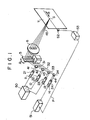
- a semiconductor laser beam device includes a plurality (four in the illustrated embodiment) of semiconductor lasers 11, 12, 13, 14 spaced laterally from each other for emitting laser beams in parallel relation to each other.
- the semiconductor lasers 11, 12, 13, 14 are associated with respective collimator lenses 21, 22, 23, 24 and respective reflecting mirrors 31, 32, 33, 34.
- the laser beams emitted from the semiconductor lasers 11, 12, 13, 14 are converted by the collimator lenses 21, 22, 23, 24 to respective parallel beams 41, 42, 43, 44, which are reflected by the reflecting mirrors 31, 32, 33, 34, respectively, toward a common galvanometer mirror 5.
- the galvanometer mirror 5 is reciprocally movable angularly in the directions of the arrow A for deflecting the parallel beams 41, 42, 43, 44 through an angular interval.
- the parallel beams are then combined by a common focusing lens 6 into a single laser beam 45, the lens causing each primary beam to converge on beam spot S.
- a surface 7 placed where the beam spot S is formed can therefore be scanned in the directions of the arrow B -by a scanning beam of. a high power which is produced by combining the laser beams emitted from the semiconductor lasers 11, 12, 13, 14.
- the surface 7 to be scanned is shown as flat, and hence the focusing lens 6 comprises an f8 lens.
- the semiconductor lasers 11, 12, 13 out of the four semiconductor lasers are energized by a constant current supplied from a constant-current laser drive circuit 50 so that the amounts of energy of the laser beams emitted from the semiconductor lasers 11, 12, 13 will remain uncontrolled.
- the remaining semiconductor laser 14 is energized by a variable current fed from a laser drive/control circuit 51 for controlling the power of the laser beam emitted from the semicondcutor laser 14.
- a laser beam energy detector 52 such as a photodiode is disposed in a position out of the effective scanning width on the surface 7 for detecting the power of the combined laser beam on the beam spot S.
- the output signal from the laser beam energy detector 52 is amplified by an amplifier 53 which applies the amplified signal as a beam energy signal P to the laser drive/control circuit 51.
- the power of the laser beams emitted from the semiconductor lasers 11, 12, 13,14 varies dependent on time-dependent changes in the characteristics of the semiconductor lasers 11, 12, 13, 14, and also with the ambient temperature and other factors, and hence the power of the combined beam at beam spot S also varies therewith.
- the power of the combined beam at beam spots is detected by the laser beam energy detector 52 in each scanning cycle.
- the tram energy signal P indicating the detected power of the combined beam of beam spot S is amplified and applied to the laser drive/control circuit 51.
- the laser drive/control circuit 51 compares the beam energy signal P with a reference beam energy signal representing a reference laser beam power. If the detected laser beam power is lower than the reference laser beam power, then the laser drive/control circuit 51 controls the semiconductor laser 14 to increase its output.
- the laser drive/control circuit 51 controls the semiconductor laser 14 to reduce its output.
- the semiconductor laser 14 is thus controlled, undesired variations in the combined laser beam power of the combined beam spot S are eliminated to keep the laser beam power constant there.
- the output of the semiconductor laser 14 may be controlled, i.e., increased and reduced, in proportion to the difference between the detected and reference laser beam power, or may be controlled to vary by small fixed amounts.
- One cycle of variations caused in the powers of the laser beams from the semiconductor lasers 11, 12, 13, 14 for the reasons given above is extremely long as compared with the period of a scanning cycle of the beam spot S. Therefore, the combined beam power of beam spot S remains virtually unchanged in one scanning cycle, and can be maintained at a constant level simply by controlling the output of the semiconductor laser 14 dependent on the combined beam power at beam spot S once in each scanning cycle. While the parallel beams 41, 42, 43, 44 are converged by the focusing lens 6 in the illustrated arrangement, the principles of the present invention are applicable to a semiconductor laser beam device in which a plurality of semiconductor lasers are arranged so that convergent laser beams emitted therefrom are combined so as to fall on a common beam spot.
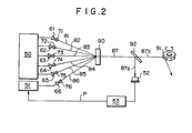
- Figure 2 shows a sem-iconductor laser beam scanning device according to a second embodiment of the present invention.
- the laser beams emitted respectively from six semiconductor lasers 61, 62, 63, 64, 65, 66 are converted by respective collimator lenses 71, 72, 73, 74, 75, 76 to convergent beams 81, 82, 83, 84, 85, 86, respectively.
- the convergent beams 81, 82, 83, 84, 85 converge toward and are combined by a hologram element 90 into a single high-power laser beam 87 which is deflected by a rotating polygonal mirror 91, for example, to scan a surface (not shown).
- the semiconductor lasers 61 through 65 out of the six semiconductor lasers are energized by a constant current supplied from a laser drive circuit 50 (identical to the laser drive circuit 50 shown in Figure 1), and the remaining semiconductor laser 66 is energized by a variable current supplied from a laser drive/control circuit 51 (identical to the laser drive/control circuit 51 illustrated in Figure 1).
- a half-silvered mirror or beam splitter 92 is positioned in the beam path for the combined beam 87 for dividing a laser beam 87a from the combined laser beam 87.
- the divided laser beam 87a falls on a laser beam energy detector 52 which detects the power of the laser beam 87a.
- the beam splitter 92 also allows a laser beam 87b to pass therethrough, the power of the laser beam 87b being proportional to that of the laser beam 87a. Therefore, the power of the laser beam 87b can be detected by detecting the power of the divided laser beam 87a with the detector 52.
- the output signal from the detector 52 is amplified by an amplifier 53 which issues a laser beam energy signal P to the laser drive/control circuit 51.
- the laser drive/control circuit 51 operates in the same manner as the laser drive/control circuit 51 in Figure 1 for controlling the power of the laser beam 87b to be kept at a constant level dependent on the laser beam energy signal P.
- other known beam combining means such as a biaxial crystal element may be employed for combining the laser beams emitted from the semiconductor lasers 61 through 66 into a single laser beam before reaching a scanning spot.
- the galvanometer mirror 5 ( Figure 1) or the polygonal mirror 91 ( Figure 2) may be replaced with a hologram scanner or the like.
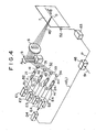
- Figure 3 shows a semiconductor laser beam scanning device according to a third embodiment of the present invention. Since the semiconductor laser beam shown in Figure 3 is similar to the semiconductor laser beam of Figure 1, the different structural details will mainly be described. As illustrated in Figure 3, four semiconductor lasers 11, 12, 13, 14 are energized by constant currents supplied from respective constant-current laser drive circuits Cl, C2, C3, C4. Since the semiconductor lasers 11 through 14 are energized by the supplied constant currents, any variation in the powers of the parallel laser beams 41 through 44 and hence in the power of the single laser beam 45 is suppressed to a certain extent.
- a control circuit D4 capable of varying the current setting in the constant-current laser drive circuit is connected to one of the constant-current laser drive circuits (C4 in the embodiment of Figure 3). Between the amplifier 53 and the control circuit D4, there is connected a comparator 51 for comparing the beam energy signal P fed from the amplifier 53 and a reference signal Sr representative of a prescribed power for the combined laser beam 45 at beam spot S.
- the power of the combined laser beam at beam spot S is detected by the laser beam energy detector 52 in each scanning cycle.
- the beam energy signal P is applied from amplifier 53 to the comparator 46 which compares the signal P with the reference signal Sr. If the beam energy signal P is greater than the reference signal Sr, i.e., if the power of the combined beam at beam spot S is higher than the prescribed power value, then the comparator 46 generates a difference signal of a high level (H). If the beam energy signal P is lower than the reference signal Sr, then the comparator 46 produces a difference signal of a low level ( L ).
- the high- or low-level difference signal (H/L) generated by the comparator 46 is applied to the control circuit D4.
- the control circuit D4 lowers the current setting in the constant-current laser drive circuit C4 so long as the high-level signal is applied to the control circuit D4.
- the laser beam output emitted from the semiconductor laser 14 is then lowered to reduce the power of the combined beam at beam spot S toward the prescribed power value.
- the control circuit D4 increases the current setting in the constant-current laser drive circuit C4 in response to the low-level signal from the comparator 46. Then, the laser beam output emitted from the semiconductor laser 14 is increased to cause the power of the combined beam at beam spot S to approach the prescribed power value.
- the laser drive circuit C4 is controlled by the control circuit D4 to vary the laser beam output from the semiconductor laser 14 so that the difference signal produced by the comparator 46 will be eliminated. Therefore, the power of the combined beam at beam spot S is kept equal to the prescribed amount of energy.
- the current setting in the constant-current laser drive circuit C4 is increased or reduced a small fixed amount by the control circuit D4.
- the comparator 51 may comprise a circuit capable of generating a signal having a level proportional to the difference between the laser beam energy signal P and the reference signal Sr, and the current setting in the constant-current laser drive circuit C4 may directly be varied by such a difference-dependent signal.
- FIG 4 illustrates a semiconductor laser beam scanning device according to a fourth embodiment of the present invention.
- the semiconductor laser beam scanning device of Figure 4 is substantially the same as the semiconductor laser beam scanning device shown in Figure 3 except that the semiconductor lasers 11, 12, 13, 14 are energized by drive currents supplied from respective constant-output laser drive circuits El, E2, E3, E4.
- the semiconductor lasers 11, 12, 13, 14 have light detectors (not shown) mounted in the laser casings, respectively, thereof for generating laser beam energy signals Sl, S2, S3, S4 which are fed back to the constant-output laser drive circuits El, E2, E3, E4, respectively.
- the constant-output laser drive circuits El through E4 control the drive currents so that the laser beam energy signals Sl through S4 will have prescribed values, i.e., the powers of the laser beams 41 through 44 will have prescribed values.
- a control circuit D4 identical to the control circuit D4 in Figure 3 is connected to the constant-output laser drive circuit E4 for controlling the drive current supplied from the laser drive circuit E4 in response to a high- or low-level signal fed from a comparator 46, identical to the comparator 46 in Figure 3, connected to the amplifier 53. Therefore, the laser beam 44 emitted from the semiconductor laser 14 is controlled to keep the power of the single laser beam 45 at a prescribed constant level.
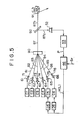
- a semiconductor laser beam scanning device differs from the semiconductor laser beam scanning device of Figure 2 in that the six semiconductor lasers 61 through 66 are energized by constant currents supplied from respective constant-current laser drive circuits Cl, C2, C3, C4, C5, C6.
- the current settings in the constant-current laser drive circuits C5, C6 can be varied by control circuits D5, D6 connected thereto, respectively, each of the control circuits D5, D6 being identical to the control circuit D4 shown in Figure 2.
- a comparator 51 identical to the comparator 46 of Figure 2, is connected between the amplifier 53 and the control circuits D5, D6.
- the beam energy signal P indicative of the power of the laser beam 87b is supplied from the amplifier 53 to the comparator 46 which compares the beam energy signal P with a reference signal Sr.
- a signal of a high or low level ( H/L ) is then issued from the comparator 46 to the control circuits D5, D6 to enable the control circuits D5, D6 to control the current settings in the drive circuits C5, C6 for varying the powers of laser beams 85, 86 emitted from the semiconductor lasers 65, 66, thus keeping the laser beam 87b at a prescribed level.
- FIG. 6 shows a semiconductor laser beam scanning device according to a sixth embodiment of the present invention.
- the semiconductor laser beam scanning device of Figure 6 is similar to the semiconductor laser beam scanning device illustrated in Figure 4.
- the semiconductor lasers 11, 12, 13 out of the four semiconductor lasers are energized by a constant current supplied from a constant-current laser drive circuit 54 identical to the laser drive.circuit 50 shown in Figure 1..
- the remaining semiconductor laser 14 is energized by a constant-output laser drive circuit 55 identical to the constant-output laser drive circuit E4 shown in Figure 4.
- the semiconductor laser 14 has a light detector mounted in the laser casing thereof for generating a laser beam energy signal S4 which is fed back to the constant-output laser drive circuit 55.
- the constant-output laser drive circuit 55 controls the drive current so that the laser beam energy signal S4 will have a prescribed value, i.e., the power of the laser beam 44 will have a prescribed value.
- a control circuit 56 identical to the control circuit D4 in Figure 4 is connected to the constant-output laser drive circuit 55 for controlling the drive current supplied from the laser drive circuit 55 in response to a high-or low level signal (H/L) fed from a comparator 46, identical to the comparator 46 in Figure 4, connected to the amplifier 53. Therefore, the laser beam 44 emitted from the semiconductor laser 14 is controlled to keep the power - y of the single laser beam 45 at a prescribed constant level.
- H/L high-or low level signal
- FIG. 7 illustrates a semiconductor laser beam scanning device according to a seventh embodiment of the present invention, which is similar to the fifth embodiment shown in Figure 5.
- the semiconductor lasers 61, 62, 63, 64, 65 out of the six semiconductor lasers are energized by a constant current supplied from a constant-current laser drive circuit 54 identical to the laser drive circuit 50 shown in Figure 1.
- the remaining semiconductor laser 66 is energized by a constant-output laser drive circuit 55 identical to the constant-output laser drive circuit 55 shown in Figure 6.
- the semiconductor laser 66 has a light detector mounted in the laser casing thereof for generating a laser beam energy signal S4 which is fed back to the constant-output laser drive circuit 55.
- the constant-output laser drive circuit 55 controls the drive current so that the laser beam energy signal S4 will have a prescribed value, i.e., the power of the laser beam 44 will have a prescribed value.
- a control circuit 56 identical to the control circuit 56 in Figure 6 is connected to the constant-output laser drive circuit 55 for controlling the drive current fed from the laser drive circuit 55 in response to a high- or-low-level signal (H/L) fed from a comparator 46, identical to the comparator 46 in Figure 6, connected to the amplifier 53.
- the laser beam 44 emitted from the semiconductor laser 66 is thus controlled to keep the power of the laser beam 87b at a prescribed constant level.
- the number of laser beams to be combined into a single laser beam is not limited to four or six as illustrated in the foregoing embodiments. Where more laser beams are combined so that the power of the combined laser beam will tend to vary to a greater extent, two or more semiconductor lasers may be controlled for varying the power of laser beams emitted therefrom to provide a wider laser beam power control range than the extent to which the power of the combined laser beam varies.
Abstract
Description
- The present invention relates to a semiconductor laser beam scanning device for combining the laser beams emitted from a plurality of semiconductor lasers into a single laser beam and for scanning the single laser beam.
- Light beam scanning devices having light deflectors for deflecting light beams for line scanning are widely used in various apparatus such as scanning recorders or printers, scanning readout apparatus, and the like. Various means for generating the light beams have heretofore been employed in the light beam scanning devices. One of the conventional light beam sources is a semiconductor laser which is smaller in size,- less costly, and lower in electric power consumption than gas lasers and other types of lasers. The semiconductor laser is also advantageous in that the emitted laser beam can be modulated directly by varying the drive current.
- However, the semiconductor laser has its own shortcoming. Its output power is low. Semiconductor laser sources now commercially available can produce light outputs ranging from 20 to 30 mW, at most, when they are continuously excited. Therefore, the semiconductor laser cannot be employed in light beam scanning devices which require a high-energy light beam to be scanned, such as scanning recorders for-recording images on low-sensitivity materials such as drawn materials, typically metal films and amorphous films.
- When certain kinds of phosphors are exposed to a radiation such as X-rays, α-rays, β-rays, γ-rays, cathode- rays or ultra-violet rays, they store a part of the energy of the radiation. Then, when the phosphor which has been exposed to the radiation is exposed to stimulating rays such as visible light, light is emitted by the phosphor in proportion to the stored energy of the radiation. A phosphor exhibiting such properties is referred to as a stimulable phosphor.
- As disclosed in Japanese Unexamined Patent Publication Nos. 55(1980)-12429, 55(1980)-116340, 55(1980)-163472, 56(1981)-11395, and 56(1981)104645, for example, it has been proposed to use a stimulable phosphor in a radiation image recording and reproducing system. Specifically, a or web provided with a layer of the stimulable phosphor (hereinafter referred to as a stimulable phosphor sheet) is first exposed to a radiation passing through an object such as a human body to have a radiation image stored thereon, and is then scanned with stimulating rays such as a laser beam which cause it to emit light in the-pattern of the stored image. The light emitted by the stimulable phosphor sheet upon stimulation thereof is photoelectrically detected and converted to an electric image signal, which is processed as desired to reproduce a visible image on a recording medium such as a photographic light-sensitive material or on a display device such as a cathode ray tube (CRT).
- It has been proposed to use a light beam scanning device having a semiconductor laser in the above radiation image recording and reproducing system for scanning the stimulable phosphor sheet to read the radiation image information stored on the stimulable phosphor sheet. It is however necessary to illuminate the phosphor with a stimulating ray of a sufficiently high energy in order to enable the stimulable phosphor sheet to emit light in response to exposure to the stimulating rays. Because of the output shortage, the light beam scanning device with the semiconductor laser has been difficult to employ in the radiation image recording and reproducing system for reading the radiation image information from the stimulable phosphor sheet.
- One way to produce a scanning light beam of a sufficiently high energy from a semiconductor laser source would be to use a plurality of semiconductor lasers and combine the laser beams emitted from the semiconductor lasers into a single laser beam. The laser beams from the respective semiconductor lasers may be combined together somewhere in the light beam paths leading to a scanning spot, or be combined together on the scanning spot. As well known in the art, the amount of energy of a laser beam emitted from a semiconductor laser varies with time-dependent changes in the characteristics of the semiconductor laser, and also with the ambient temperature and various other factors. Therefore, it would be necessary to control the combined single laser beam for a constant amount of laser beam energy. It has been known to detect the amount of energy of a laser beam with a laser beam energy detector and feed a signal from the detector back to a laser beam energy control circuit for controlling the amount of energy of the emitted laser beam to keep it constant. However, such a conventional laser beam energy control arrangement would be disadvantageous if used with a plurality of semiconductor lasers for generating a single combined laser beam since there would be required as many laser beam energy detectors and control circuits as the number of semiconductor lasers employed, resulting in a large and expensive light beam scanning device.
- It is an object of the present invention to provide a semiconductor laser beam scanning device which is capable of keeping constant the amount of energy of a single laser beam produced by combining the laser beams emitted from a plurality of semiconductor lasers.
- According to the present invention there is provided a semiconductor laser beam scanning device comprising:
- i) a plurality of semiconductor lasers for emitting a respective plurality of primary laser beams;
- ii) combining means for combining said primary laser beams into a single combined laser beam;
- iii) scanning means for scanning a surface with said combined laser beam;
- (iv) detecting means for detecting the power of said combined laser beam; and
- v) control means responsive to a detected signal from said detecting means for controllably energizing at least one of said semiconductor lasers to control the power of the primary laser beam emitted therefrom and thereby maintain substantially constant the power of said combined laser beam.
- With this arrangement, the power of the single combined laser beam which scans the surface is maintained at a desired constant level by controlling the power of the primary laser beam emitted from one or more, but not all, of the semiconductor lasers. Since the control means is not required to control all of the semiconductor lasers, it is simple in arrangement, and hence the semiconductor laser beam scanning device is small in size and inexpensive to manufacture.
- The above and other objects, features and advantages of the present invention will become more apparent from the following description when taken in conjunction with the accompanying drawings in-which- preferred embodiments of the present invention are shown by way of illustrative example.
-
- Figure 1 is a schematic perspective view of a semiconductor laser beam scanning device according to a first embodiment of the present invention;
- Figure 2 is a schematic view of a semiconductor laser beam scanning device according to a second embodiment of the present invention;
- Figure 3 is schematic perspective view of a semiconductor laser beam scanning device according to a third embodiment of the present invention;
- Figure 4 is schematic perspective view of a semiconductor laser beam scanning device according to a fourth embodiment of the present invention;
- Figure 5 is schematic view of a semiconductor laser beam scanning device according to a fifth embodiment of the present invention;
- Figure 6 is schematic perspective view of a semiconductor laser beam scanning device according to a sixth embodiment of the present invention;
- Figure 7 is schematic view of a semiconductor laser beam scanning device according to a seventh embodiment of the present invention.
- Identical or corresponding parts are denoted by identical or corresponding reference characters throughout the views.
- As shown in Figure 1, a semiconductor laser beam device according to a first embodiment of the present invention includes a plurality (four in the illustrated embodiment) of
semiconductor lasers semiconductor lasers respective collimator lenses mirrors semiconductor lasers collimator lenses parallel beams mirrors - The galvanometer mirror 5 is reciprocally movable angularly in the directions of the arrow A for deflecting the
parallel beams lens 6 into asingle laser beam 45, the lens causing each primary beam to converge on beam spot S. A surface 7 placed where the beam spot S is formed can therefore be scanned in the directions of the arrow B -by a scanning beam of. a high power which is produced by combining the laser beams emitted from thesemiconductor lasers lens 6 comprises an f8 lens. - The
semiconductor lasers laser drive circuit 50 so that the amounts of energy of the laser beams emitted from thesemiconductor lasers remaining semiconductor laser 14 is energized by a variable current fed from a laser drive/control circuit 51 for controlling the power of the laser beam emitted from thesemicondcutor laser 14. A laserbeam energy detector 52 such as a photodiode is disposed in a position out of the effective scanning width on the surface 7 for detecting the power of the combined laser beam on the beam spot S. The output signal from the laserbeam energy detector 52 is amplified by anamplifier 53 which applies the amplified signal as a beam energy signal P to the laser drive/control circuit 51. - As mentioned above, the power of the laser beams emitted from the
semiconductor lasers semiconductor lasers beam energy detector 52 in each scanning cycle. The tram energy signal P indicating the detected power of the combined beam of beam spot S is amplified and applied to the laser drive/control circuit 51. The laser drive/control circuit 51 compares the beam energy signal P with a reference beam energy signal representing a reference laser beam power. If the detected laser beam power is lower than the reference laser beam power, then the laser drive/control circuit 51 controls thesemiconductor laser 14 to increase its output. Conversely, if the detected laser beam power is higher than the reference laser beam power, then the laser drive/control circuit 51 controls thesemiconductor laser 14 to reduce its output. When thesemiconductor laser 14 is thus controlled, undesired variations in the combined laser beam power of the combined beam spot S are eliminated to keep the laser beam power constant there. The output of thesemiconductor laser 14 may be controlled, i.e., increased and reduced, in proportion to the difference between the detected and reference laser beam power, or may be controlled to vary by small fixed amounts. - One cycle of variations caused in the powers of the laser beams from the
semiconductor lasers semiconductor laser 14 dependent on the combined beam power at beam spot S once in each scanning cycle. While theparallel beams lens 6 in the illustrated arrangement, the principles of the present invention are applicable to a semiconductor laser beam device in which a plurality of semiconductor lasers are arranged so that convergent laser beams emitted therefrom are combined so as to fall on a common beam spot. - Figure 2 shows a sem-iconductor laser beam scanning device according to a second embodiment of the present invention. As shown in Figure 2, the laser beams emitted respectively from six
semiconductor lasers respective collimator lenses convergent beams convergent beams hologram element 90 into a single high-power laser beam 87 which is deflected by a rotatingpolygonal mirror 91, for example, to scan a surface (not shown). - The
semiconductor lasers 61 through 65 out of the six semiconductor lasers are energized by a constant current supplied from a laser drive circuit 50 (identical to thelaser drive circuit 50 shown in Figure 1), and the remainingsemiconductor laser 66 is energized by a variable current supplied from a laser drive/control circuit 51 (identical to the laser drive/control circuit 51 illustrated in Figure 1). A half-silvered mirror orbeam splitter 92 is positioned in the beam path for the combinedbeam 87 for dividing alaser beam 87a from the combinedlaser beam 87. The dividedlaser beam 87a falls on a laserbeam energy detector 52 which detects the power of thelaser beam 87a. Thebeam splitter 92 also allows alaser beam 87b to pass therethrough, the power of thelaser beam 87b being proportional to that of thelaser beam 87a. Therefore, the power of thelaser beam 87b can be detected by detecting the power of the dividedlaser beam 87a with thedetector 52. The output signal from thedetector 52 is amplified by anamplifier 53 which issues a laser beam energy signal P to the laser drive/control circuit 51. The laser drive/control circuit 51 operates in the same manner as the laser drive/control circuit 51 in Figure 1 for controlling the power of thelaser beam 87b to be kept at a constant level dependent on the laser beam energy signal P. - Instead of the
hologram element 90, .other known beam combining means such as a biaxial crystal element may be employed for combining the laser beams emitted from thesemiconductor lasers 61 through 66 into a single laser beam before reaching a scanning spot. The galvanometer mirror 5 (Figure 1) or the polygonal mirror 91 (Figure 2) may be replaced with a hologram scanner or the like. - Figure 3 shows a semiconductor laser beam scanning device according to a third embodiment of the present invention. Since the semiconductor laser beam shown in Figure 3 is similar to the semiconductor laser beam of Figure 1, the different structural details will mainly be described. As illustrated in Figure 3, four
semiconductor lasers semiconductor lasers 11 through 14 are energized by the supplied constant currents, any variation in the powers of theparallel laser beams 41 through 44 and hence in the power of thesingle laser beam 45 is suppressed to a certain extent. To prevent the power of thesingle laser beam 45 from being varied, a control circuit D4 capable of varying the current setting in the constant-current laser drive circuit is connected to one of the constant-current laser drive circuits (C4 in the embodiment of Figure 3). Between theamplifier 53 and the control circuit D4, there is connected acomparator 51 for comparing the beam energy signal P fed from theamplifier 53 and a reference signal Sr representative of a prescribed power for the combinedlaser beam 45 at beam spot S. - In operation, the power of the combined laser beam at beam spot S is detected by the laser
beam energy detector 52 in each scanning cycle. The beam energy signal P is applied fromamplifier 53 to thecomparator 46 which compares the signal P with the reference signal Sr. If the beam energy signal P is greater than the reference signal Sr, i.e., if the power of the combined beam at beam spot S is higher than the prescribed power value, then thecomparator 46 generates a difference signal of a high level (H). If the beam energy signal P is lower than the reference signal Sr, then thecomparator 46 produces a difference signal of a low level (L). - The high- or low-level difference signal (H/L) generated by the
comparator 46 is applied to the control circuit D4. The control circuit D4 lowers the current setting in the constant-current laser drive circuit C4 so long as the high-level signal is applied to the control circuit D4. The laser beam output emitted from thesemiconductor laser 14 is then lowered to reduce the power of the combined beam at beam spot S toward the prescribed power value. Conversely, the control circuit D4 increases the current setting in the constant-current laser drive circuit C4 in response to the low-level signal from thecomparator 46. Then, the laser beam output emitted from thesemiconductor laser 14 is increased to cause the power of the combined beam at beam spot S to approach the prescribed power value. Stated otherwise, the laser drive circuit C4 is controlled by the control circuit D4 to vary the laser beam output from thesemiconductor laser 14 so that the difference signal produced by thecomparator 46 will be eliminated. Therefore, the power of the combined beam at beam spot S is kept equal to the prescribed amount of energy. The current setting in the constant-current laser drive circuit C4 is increased or reduced a small fixed amount by the control circuit D4. However, thecomparator 51 may comprise a circuit capable of generating a signal having a level proportional to the difference between the laser beam energy signal P and the reference signal Sr, and the current setting in the constant-current laser drive circuit C4 may directly be varied by such a difference-dependent signal. - Figure 4 illustrates a semiconductor laser beam scanning device according to a fourth embodiment of the present invention. The semiconductor laser beam scanning device of Figure 4 is substantially the same as the semiconductor laser beam scanning device shown in Figure 3 except that the
semiconductor lasers semiconductor lasers laser beams 41 through 44 will have prescribed values. A control circuit D4 identical to the control circuit D4 in Figure 3 is connected to the constant-output laser drive circuit E4 for controlling the drive current supplied from the laser drive circuit E4 in response to a high- or low-level signal fed from acomparator 46, identical to thecomparator 46 in Figure 3, connected to theamplifier 53. Therefore, thelaser beam 44 emitted from thesemiconductor laser 14 is controlled to keep the power of thesingle laser beam 45 at a prescribed constant level. - A semiconductor laser beam scanning device according to a fifth embodiment shown in Figure 5 differs from the semiconductor laser beam scanning device of Figure 2 in that the six
semiconductor lasers 61 through 66 are energized by constant currents supplied from respective constant-current laser drive circuits Cl, C2, C3, C4, C5, C6. The current settings in the constant-current laser drive circuits C5, C6 can be varied by control circuits D5, D6 connected thereto, respectively, each of the control circuits D5, D6 being identical to the control circuit D4 shown in Figure 2. Acomparator 51, identical to thecomparator 46 of Figure 2, is connected between theamplifier 53 and the control circuits D5, D6. The beam energy signal P indicative of the power of thelaser beam 87b is supplied from theamplifier 53 to thecomparator 46 which compares the beam energy signal P with a reference signal Sr. A signal of a high or low level (H/L) is then issued from thecomparator 46 to the control circuits D5, D6 to enable the control circuits D5, D6 to control the current settings in the drive circuits C5, C6 for varying the powers oflaser beams semiconductor lasers laser beam 87b at a prescribed level. - Figure 6 shows a semiconductor laser beam scanning device according to a sixth embodiment of the present invention. The semiconductor laser beam scanning device of Figure 6 is similar to the semiconductor laser beam scanning device illustrated in Figure 4. The
semiconductor lasers laser drive circuit 54 identical to thelaser drive.circuit 50 shown in Figure 1.. The remainingsemiconductor laser 14 is energized by a constant-outputlaser drive circuit 55 identical to the constant-output laser drive circuit E4 shown in Figure 4. Thesemiconductor laser 14 has a light detector mounted in the laser casing thereof for generating a laser beam energy signal S4 which is fed back to the constant-outputlaser drive circuit 55. In response to the laser beam energy signal S4, the constant-outputlaser drive circuit 55 controls the drive current so that the laser beam energy signal S4 will have a prescribed value, i.e., the power of thelaser beam 44 will have a prescribed value. Acontrol circuit 56 identical to the control circuit D4 in Figure 4 is connected to the constant-outputlaser drive circuit 55 for controlling the drive current supplied from thelaser drive circuit 55 in response to a high-or low level signal (H/L) fed from acomparator 46, identical to thecomparator 46 in Figure 4, connected to theamplifier 53. Therefore, thelaser beam 44 emitted from thesemiconductor laser 14 is controlled to keep the power - y of thesingle laser beam 45 at a prescribed constant level. - Figure 7 illustrates a semiconductor laser beam scanning device according to a seventh embodiment of the present invention, which is similar to the fifth embodiment shown in Figure 5. The
semiconductor lasers laser drive circuit 54 identical to thelaser drive circuit 50 shown in Figure 1. The remainingsemiconductor laser 66 is energized by a constant-outputlaser drive circuit 55 identical to the constant-outputlaser drive circuit 55 shown in Figure 6. Thesemiconductor laser 66 has a light detector mounted in the laser casing thereof for generating a laser beam energy signal S4 which is fed back to the constant-outputlaser drive circuit 55. In response to the laser beam energy signal S4, the constant-outputlaser drive circuit 55 controls the drive current so that the laser beam energy signal S4 will have a prescribed value, i.e., the power of thelaser beam 44 will have a prescribed value. Acontrol circuit 56 identical to thecontrol circuit 56 in Figure 6 is connected to the constant-outputlaser drive circuit 55 for controlling the drive current fed from thelaser drive circuit 55 in response to a high- or-low-level signal (H/L) fed from acomparator 46, identical to thecomparator 46 in Figure 6, connected to theamplifier 53. Thelaser beam 44 emitted from thesemiconductor laser 66 is thus controlled to keep the power of thelaser beam 87b at a prescribed constant level. - The number of laser beams to be combined into a single laser beam is not limited to four or six as illustrated in the foregoing embodiments. Where more laser beams are combined so that the power of the combined laser beam will tend to vary to a greater extent, two or more semiconductor lasers may be controlled for varying the power of laser beams emitted therefrom to provide a wider laser beam power control range than the extent to which the power of the combined laser beam varies.
Claims (11)
Applications Claiming Priority (6)
| Application Number | Priority Date | Filing Date | Title |
|---|---|---|---|
| JP59121089A JPS60264158A (en) | 1984-06-13 | 1984-06-13 | Semiconductor laser scanning device |
| JP121089/84 | 1984-06-13 | ||
| JP60119315A JPS61275870A (en) | 1985-05-31 | 1985-05-31 | Controller for quantity of light of semiconductor laser light source |
| JP119315/85 | 1985-05-31 | ||
| JP119316/85 | 1985-05-31 | ||
| JP11931685A JPS61275871A (en) | 1985-05-31 | 1985-05-31 | Controller for quantity of light of semiconductor laser light source |
Publications (3)
| Publication Number | Publication Date |
|---|---|
| EP0165060A2 true EP0165060A2 (en) | 1985-12-18 |
| EP0165060A3 EP0165060A3 (en) | 1988-09-21 |
| EP0165060B1 EP0165060B1 (en) | 1991-09-04 |
Family
ID=27313790
Family Applications (1)
| Application Number | Title | Priority Date | Filing Date |
|---|---|---|---|
| EP85304186A Expired EP0165060B1 (en) | 1984-06-13 | 1985-06-12 | Semiconductor laser beam scanning device |
Country Status (3)
| Country | Link |
|---|---|
| US (1) | US4689482A (en) |
| EP (1) | EP0165060B1 (en) |
| DE (1) | DE3583969D1 (en) |
Cited By (11)
| Publication number | Priority date | Publication date | Assignee | Title |
|---|---|---|---|---|
| EP0272325A4 (en) * | 1986-06-30 | 1988-06-27 | Medical Laser Res Co Ltd | Semiconductor laser therapeutic apparatus. |
| EP0321143A2 (en) * | 1987-12-17 | 1989-06-21 | AT&T Corp. | Method and apparatus for direct color printing |
| EP0358171A2 (en) * | 1988-09-06 | 1990-03-14 | Canon Kabushiki Kaisha | Light intensity control apparatus |
| EP0415903A2 (en) * | 1989-08-30 | 1991-03-06 | Polaroid Corporation | Imaging recorder |
| WO1991004596A1 (en) * | 1989-09-14 | 1991-04-04 | Australian Electro Optics Pty. Ltd. | Phase-locked multi slab array laser |
| EP0529531A2 (en) * | 1991-08-23 | 1993-03-03 | Eastman Kodak Company | Methods for measuring laser performance in laser printers |
| GB2290655A (en) * | 1994-06-22 | 1996-01-03 | Eastman Kodak Co | High dynamic range laser diode direct modulation |
| FR2734902A1 (en) * | 1995-05-30 | 1996-12-06 | Asahi Optical Co Ltd | LIGHT INTENSITY CONTROL DEVICE |
| EP0887679A2 (en) * | 1997-06-23 | 1998-12-30 | Kabushiki Kaisha Toshiba | Inclination adjusting device for light controlling element used in optical scanner |
| US6398801B1 (en) | 1996-05-29 | 2002-06-04 | Icn Photonics Limited | Treatment of vascular lesions |
| US6605083B2 (en) | 1996-05-29 | 2003-08-12 | Robert Marc Clement | Reduction of vascular blemishes by selective thermolysis |
Families Citing this family (55)
| Publication number | Priority date | Publication date | Assignee | Title |
|---|---|---|---|---|
| JPS60220308A (en) * | 1984-04-17 | 1985-11-05 | Fuji Photo Film Co Ltd | Optical beam scanner |
| DE68924286T2 (en) * | 1988-02-18 | 1996-02-29 | Fuji Photo Film Co Ltd | Method and apparatus for reading and reproducing images and light source device for several semiconductor lasers therefor. |
| US4992803A (en) * | 1988-12-21 | 1991-02-12 | The Mead Corporation | Simultaneous laser writing of multiple LALC cells |
| JP2913179B2 (en) * | 1989-05-15 | 1999-06-28 | 株式会社リコー | Scan beam output control device |
| US5185758A (en) * | 1989-11-28 | 1993-02-09 | Massachusetts Institute Of Technology | Multiple-laser pump optical system |
| US5081637A (en) * | 1989-11-28 | 1992-01-14 | Massachusetts Institute Of Technology | Multiple-laser pump optical system |
| JP2505293B2 (en) * | 1989-12-08 | 1996-06-05 | 日本たばこ産業株式会社 | Perforator |
| ATE190733T1 (en) * | 1990-08-01 | 2000-04-15 | Diomed Ltd | HIGH POWER LIGHT SOURCE |
| JPH04316276A (en) * | 1991-04-16 | 1992-11-06 | Ricoh Co Ltd | Image forming device |
| CA2155310A1 (en) * | 1993-02-03 | 1994-08-18 | Frank C. Gibeau | Methods and apparatus for image projection |
| EP0700325B1 (en) * | 1993-05-19 | 1997-08-13 | Fraunhofer-Gesellschaft Zur Förderung Der Angewandten Forschung E.V. | Method for machining materials by diode radiation |
| JPH07140572A (en) * | 1993-11-22 | 1995-06-02 | Fuji Photo Film Co Ltd | Radiation image information reader |
| US5602402A (en) * | 1994-10-14 | 1997-02-11 | Fuji Photo Film Co., Ltd. | Radiation image read-out method and apparatus |
| JP3141715B2 (en) * | 1994-12-22 | 2001-03-05 | 松下電器産業株式会社 | Laser processing method |
| US5691535A (en) * | 1996-02-08 | 1997-11-25 | Eastman Kodak Company | Ganged laser scanning system which corrects beam alignment along a bow-tie path |
| US5701003A (en) * | 1996-10-22 | 1997-12-23 | Computer Identics Corporation | Intensity compensated scanning system |
| US6239888B1 (en) | 1998-04-24 | 2001-05-29 | Lightpointe Communications, Inc. | Terrestrial optical communication network of integrated fiber and free-space links which requires no electro-optical conversion between links |
| US6868237B2 (en) | 1998-04-24 | 2005-03-15 | Lightpointe Communications, Inc. | Terrestrial optical communication network of integrated fiber and free-space links which requires no electro-optical conversion between links |
| US6303917B1 (en) | 1999-05-14 | 2001-10-16 | Ultratech Stepper, Inc. | Radiant energy monitoring apparatuses including a calibration operation and related methods |
| AU5285901A (en) * | 1999-10-25 | 2001-07-03 | Interwoven Technologies Corporation | System and method for characterizing and identifying agents |
| US7671295B2 (en) * | 2000-01-10 | 2010-03-02 | Electro Scientific Industries, Inc. | Processing a memory link with a set of at least two laser pulses |
| US6763195B1 (en) | 2000-01-13 | 2004-07-13 | Lightpointe Communications, Inc. | Hybrid wireless optical and radio frequency communication link |
| US7102700B1 (en) * | 2000-09-02 | 2006-09-05 | Magic Lantern Llc | Laser projection system |
| DE10053101A1 (en) * | 2000-10-26 | 2002-01-24 | Agfa Gevaert Ag | Process uses combined operation of two lasers with total energy sensed and used to control lasers |
| US6889009B2 (en) * | 2001-04-16 | 2005-05-03 | Lightpointe Communications, Inc. | Integrated environmental control and management system for free-space optical communication systems |
| US20020171896A1 (en) * | 2001-05-21 | 2002-11-21 | Lightpointe Communications, Inc. | Free-space optical communication system employing wavelength conversion |
| US20030090765A1 (en) * | 2001-11-09 | 2003-05-15 | Neff Brian W. | Free-space optical communication system |
| KR100459899B1 (en) * | 2002-03-12 | 2004-12-04 | 삼성전자주식회사 | Laser video projector having multi-channel acoustic optic modulator, method and circuit of driving the same |
| US20040026302A1 (en) * | 2002-08-12 | 2004-02-12 | Jack Lee | Water filter assembly |
| US7106973B2 (en) * | 2002-08-13 | 2006-09-12 | Lightpointe Communications, Inc. | Apparatus and method for use in free-space optical communication comprising optically aligned components integrated on circuit boards |
| US20040120717A1 (en) * | 2002-12-18 | 2004-06-24 | Lightpointe Communications, Inc. | Extended source free-space optical communication system |
| WO2005055675A2 (en) * | 2003-11-28 | 2005-06-16 | Alara, Inc. | Method and apparatus for improved energy readout |
| US7133061B2 (en) * | 2004-06-14 | 2006-11-07 | Texas Instruments Incorporated | Multilaser bi-directional printer with an oscillating scanning mirror |
| US7408567B2 (en) * | 2005-03-29 | 2008-08-05 | Kabushiki Kaisha Toshiba | Light beam scanning apparatus and image forming apparatus |
| JP2006317681A (en) * | 2005-05-12 | 2006-11-24 | Canon Inc | Image display device |
| US7253386B2 (en) * | 2005-12-12 | 2007-08-07 | Xerox Corporation | Method and apparatus for monitoring and controlling laser intensity in a ROS scanning system |
| JP5457031B2 (en) * | 2006-09-29 | 2014-04-02 | パナソニック株式会社 | Laser light emitting device and image display device using the same |
| WO2008058671A2 (en) * | 2006-11-14 | 2008-05-22 | Osram Gesellschaft mit beschränkter Haftung | Projection apparatus having improved projection properties |
| DE102007052103A1 (en) * | 2007-10-31 | 2009-05-07 | Medizinisches Laserzentrum Lübeck GmbH | Device for gentle laser therapy of the retina |
| US8891579B1 (en) * | 2011-12-16 | 2014-11-18 | Nlight Photonics Corporation | Laser diode apparatus utilizing reflecting slow axis collimators |
| EP2799823B1 (en) * | 2011-12-27 | 2016-12-07 | Mitsubishi Electric Corporation | Laser output measuring apparatus |
| US9346122B1 (en) | 2013-01-08 | 2016-05-24 | Universal Laser Systems, Inc. | Multi-wavelength laser processing systems and associated methods of use and manufacture |
| US9720145B2 (en) | 2014-03-06 | 2017-08-01 | Nlight, Inc. | High brightness multijunction diode stacking |
| US9705289B2 (en) | 2014-03-06 | 2017-07-11 | Nlight, Inc. | High brightness multijunction diode stacking |
| US10761276B2 (en) | 2015-05-15 | 2020-09-01 | Nlight, Inc. | Passively aligned crossed-cylinder objective assembly |
| CN108885349A (en) | 2016-02-16 | 2018-11-23 | 恩耐公司 | For improving the unimodule telescope of the packaging passive alignment of package brightness |
| WO2017161334A1 (en) | 2016-03-18 | 2017-09-21 | Nlight, Inc. | Spectrally multiplexing diode pump modules to improve brightness |
| WO2018119125A1 (en) | 2016-12-23 | 2018-06-28 | Nlight, Inc. | Low cost optical pump laser package |
| WO2018200587A1 (en) | 2017-04-24 | 2018-11-01 | Nlight, Inc. | Low swap two-phase cooled diode laser package |
| CN111919352A (en) | 2018-02-06 | 2020-11-10 | 恩耐公司 | Diode laser device with FAC lens out-of-plane beam steering |
| JP2021519841A (en) | 2018-03-30 | 2021-08-12 | ベクトン・ディキンソン・アンド・カンパニーBecton, Dickinson And Company | Water-soluble polymer dye with pendant chromophore |
| JP2021522489A (en) * | 2018-04-24 | 2021-08-30 | ベクトン・ディキンソン・アンド・カンパニーBecton, Dickinson And Company | Multiple laser system with modified beam profile and how to use it |
| EP3814748A4 (en) | 2018-06-28 | 2022-03-30 | Becton, Dickinson and Company | Integrated pre-amplification light detection systems and methods of use thereof |
| WO2021079822A1 (en) | 2019-10-24 | 2021-04-29 | 京セラ株式会社 | Power receiving device for optical power feed system, power feed device, and optical power feed system |
| US11733534B2 (en) | 2021-01-21 | 2023-08-22 | AdlOptica Optical Systems GmbH | Optics for formation of multiple light spots with controlled spot intensity and variable spot pattern geometry |
Citations (2)
| Publication number | Priority date | Publication date | Assignee | Title |
|---|---|---|---|---|
| DE3143571A1 (en) * | 1980-11-04 | 1982-07-29 | Canon K.K., Tokyo | Method and device for regulating the quantity of light of a light source arranged in a row |
| JPS5919252A (en) * | 1982-07-21 | 1984-01-31 | Ricoh Co Ltd | Control method of semiconductor laser array output |
Family Cites Families (1)
| Publication number | Priority date | Publication date | Assignee | Title |
|---|---|---|---|---|
| US3668984A (en) * | 1970-05-04 | 1972-06-13 | Harris Intertype Corp | Optical character spacing system for phototypesetting |
-
1985
- 1985-06-12 EP EP85304186A patent/EP0165060B1/en not_active Expired
- 1985-06-12 DE DE8585304186T patent/DE3583969D1/en not_active Expired - Lifetime
- 1985-06-13 US US06/744,413 patent/US4689482A/en not_active Expired - Lifetime
Patent Citations (2)
| Publication number | Priority date | Publication date | Assignee | Title |
|---|---|---|---|---|
| DE3143571A1 (en) * | 1980-11-04 | 1982-07-29 | Canon K.K., Tokyo | Method and device for regulating the quantity of light of a light source arranged in a row |
| JPS5919252A (en) * | 1982-07-21 | 1984-01-31 | Ricoh Co Ltd | Control method of semiconductor laser array output |
Non-Patent Citations (1)
| Title |
|---|
| PATENT ABSTRACTS OF JAPAN, vol. 8, no. 109 (P-275)[1546], 22nd May 1984; & JP-A-59 019 252 (RICOH K.K.) 31.01.1984 * |
Cited By (24)
| Publication number | Priority date | Publication date | Assignee | Title |
|---|---|---|---|---|
| EP0272325A4 (en) * | 1986-06-30 | 1988-06-27 | Medical Laser Res Co Ltd | Semiconductor laser therapeutic apparatus. |
| EP0272325A1 (en) * | 1986-06-30 | 1988-06-29 | MEDICAL LASER RESEARCH Co., LTD. | Semiconductor laser therapeutic apparatus |
| EP0321143A2 (en) * | 1987-12-17 | 1989-06-21 | AT&T Corp. | Method and apparatus for direct color printing |
| EP0321143A3 (en) * | 1987-12-17 | 1991-05-02 | AT&T Corp. | Method and apparatus for direct color printing |
| EP0358171A2 (en) * | 1988-09-06 | 1990-03-14 | Canon Kabushiki Kaisha | Light intensity control apparatus |
| EP0358171A3 (en) * | 1988-09-06 | 1990-09-12 | Canon Kabushiki Kaisha | Light intensity control apparatus |
| US5043745A (en) * | 1988-09-06 | 1991-08-27 | Canon Kabushiki Kaisha | Light intensity control apparatus |
| EP0415903A2 (en) * | 1989-08-30 | 1991-03-06 | Polaroid Corporation | Imaging recorder |
| EP0415903A3 (en) * | 1989-08-30 | 1991-06-05 | Polaroid Corporation | Imaging recorder |
| WO1991004596A1 (en) * | 1989-09-14 | 1991-04-04 | Australian Electro Optics Pty. Ltd. | Phase-locked multi slab array laser |
| EP0529531A2 (en) * | 1991-08-23 | 1993-03-03 | Eastman Kodak Company | Methods for measuring laser performance in laser printers |
| EP0529531A3 (en) * | 1991-08-23 | 1993-07-28 | Eastman Kodak Company | Methods for measuring laser performance in laser printers |
| GB2290655A (en) * | 1994-06-22 | 1996-01-03 | Eastman Kodak Co | High dynamic range laser diode direct modulation |
| GB2290655B (en) * | 1994-06-22 | 1998-01-21 | Eastman Kodak Co | High dynamic range laser diode direct modulation |
| FR2734902A1 (en) * | 1995-05-30 | 1996-12-06 | Asahi Optical Co Ltd | LIGHT INTENSITY CONTROL DEVICE |
| GB2301701A (en) * | 1995-05-30 | 1996-12-11 | Asahi Optical Co Ltd | Light intensity control |
| US5892219A (en) * | 1995-05-30 | 1999-04-06 | Asahi Kogaku Kogyo Kabushiki Kaisha | Light intensity controlling device |
| GB2301701B (en) * | 1995-05-30 | 1999-11-17 | Asahi Optical Co Ltd | Light power detecting device |
| US6011250A (en) * | 1995-05-30 | 2000-01-04 | Asahi Kogaku Kogyo Kabushiki Kaisha | Light intensity controlling device |
| DE19621802B4 (en) * | 1995-05-30 | 2005-12-08 | Pentax Corp. | Device for controlling the radiation intensity |
| US6398801B1 (en) | 1996-05-29 | 2002-06-04 | Icn Photonics Limited | Treatment of vascular lesions |
| US6605083B2 (en) | 1996-05-29 | 2003-08-12 | Robert Marc Clement | Reduction of vascular blemishes by selective thermolysis |
| EP0887679A2 (en) * | 1997-06-23 | 1998-12-30 | Kabushiki Kaisha Toshiba | Inclination adjusting device for light controlling element used in optical scanner |
| EP0887679A3 (en) * | 1997-06-23 | 2000-05-10 | Kabushiki Kaisha Toshiba | Inclination adjusting device for light controlling element used in optical scanner |
Also Published As
| Publication number | Publication date |
|---|---|
| EP0165060B1 (en) | 1991-09-04 |
| US4689482A (en) | 1987-08-25 |
| DE3583969D1 (en) | 1991-10-10 |
| EP0165060A3 (en) | 1988-09-21 |
Similar Documents
| Publication | Publication Date | Title |
|---|---|---|
| EP0165060B1 (en) | Semiconductor laser beam scanning device | |
| US4681394A (en) | Light beam scanning system | |
| EP0144963B1 (en) | Radiation image read-out apparatus | |
| US5072119A (en) | Radiation image read-out apparatus and erasing apparatus | |
| US4958893A (en) | Semiconductor laser beam source apparatus | |
| US4985629A (en) | Shading elmination method for an image read-out apparatus | |
| US4855597A (en) | Radiation image read-out apparatus | |
| US4841147A (en) | Image read-out and recording apparatus | |
| US5386124A (en) | Image scanning apparatus | |
| US4661708A (en) | Radiation image read-out apparatus | |
| CA1223982A (en) | Radiation image read-out apparatus | |
| US5488489A (en) | Image read-out and reproducing apparatus | |
| US4984015A (en) | Exposure method and apparatus | |
| US4908511A (en) | Light beam scanning device | |
| US4857733A (en) | Radiation image read-out method and apparatus, and radiation image read-out and reproducing method and apparatus | |
| JPH0444751B2 (en) | ||
| US5051588A (en) | Radiation image read-out apparatus | |
| JPH0685361A (en) | Semiconductor laser light source device | |
| US4967073A (en) | Light scanning device having a synchronizing grid with a phase-detected starting point area | |
| US5081356A (en) | Image read-out apparatus | |
| JPS60264158A (en) | Semiconductor laser scanning device | |
| JPH0477911B2 (en) | ||
| JPH0477910B2 (en) | ||
| JPH0260163B2 (en) | ||
| JP2903269B2 (en) | Optical scanning device and photoreceptor |
Legal Events
| Date | Code | Title | Description |
|---|---|---|---|
| PUAI | Public reference made under article 153(3) epc to a published international application that has entered the european phase |
Free format text: ORIGINAL CODE: 0009012 |
|
| AK | Designated contracting states |
Designated state(s): DE FR NL |
|
| PUAL | Search report despatched |
Free format text: ORIGINAL CODE: 0009013 |
|
| AK | Designated contracting states |
Kind code of ref document: A3 Designated state(s): DE FR NL |
|
| 17P | Request for examination filed |
Effective date: 19881222 |
|
| 17Q | First examination report despatched |
Effective date: 19901211 |
|
| GRAA | (expected) grant |
Free format text: ORIGINAL CODE: 0009210 |
|
| AK | Designated contracting states |
Kind code of ref document: B1 Designated state(s): DE FR NL |
|
| REF | Corresponds to: |
Ref document number: 3583969 Country of ref document: DE Date of ref document: 19911010 |
|
| ET | Fr: translation filed | ||
| PLBE | No opposition filed within time limit |
Free format text: ORIGINAL CODE: 0009261 |
|
| STAA | Information on the status of an ep patent application or granted ep patent |
Free format text: STATUS: NO OPPOSITION FILED WITHIN TIME LIMIT |
|
| 26N | No opposition filed | ||
| PGFP | Annual fee paid to national office [announced via postgrant information from national office to epo] |
Ref country code: NL Payment date: 20040517 Year of fee payment: 20 |
|
| PGFP | Annual fee paid to national office [announced via postgrant information from national office to epo] |
Ref country code: FR Payment date: 20040618 Year of fee payment: 20 |
|
| PGFP | Annual fee paid to national office [announced via postgrant information from national office to epo] |
Ref country code: DE Payment date: 20040802 Year of fee payment: 20 |
|
| PG25 | Lapsed in a contracting state [announced via postgrant information from national office to epo] |
Ref country code: NL Free format text: LAPSE BECAUSE OF EXPIRATION OF PROTECTION Effective date: 20050612 |
|
| NLV7 | Nl: ceased due to reaching the maximum lifetime of a patent |
Effective date: 20050612 |