EP0163060A2 - Surface acoustic wave infrared line imaging array - Google Patents
Surface acoustic wave infrared line imaging array Download PDFInfo
- Publication number
- EP0163060A2 EP0163060A2 EP85103995A EP85103995A EP0163060A2 EP 0163060 A2 EP0163060 A2 EP 0163060A2 EP 85103995 A EP85103995 A EP 85103995A EP 85103995 A EP85103995 A EP 85103995A EP 0163060 A2 EP0163060 A2 EP 0163060A2
- Authority
- EP
- European Patent Office
- Prior art keywords
- surface acoustic
- acoustic wave
- interdigital transducer
- line imaging
- wave train
- Prior art date
- Legal status (The legal status is an assumption and is not a legal conclusion. Google has not performed a legal analysis and makes no representation as to the accuracy of the status listed.)
- Withdrawn
Links
- 238000010897 surface acoustic wave method Methods 0.000 title claims abstract description 48
- 238000003384 imaging method Methods 0.000 title claims abstract description 43
- 239000000758 substrate Substances 0.000 claims abstract description 33
- 238000003491 array Methods 0.000 claims description 14
- 230000008878 coupling Effects 0.000 claims description 7
- 238000010168 coupling process Methods 0.000 claims description 7
- 238000005859 coupling reaction Methods 0.000 claims description 7
- 230000001419 dependent effect Effects 0.000 claims description 4
- 238000003331 infrared imaging Methods 0.000 description 4
- GQYHUHYESMUTHG-UHFFFAOYSA-N lithium niobate Chemical compound [Li+].[O-][Nb](=O)=O GQYHUHYESMUTHG-UHFFFAOYSA-N 0.000 description 3
- 238000000034 method Methods 0.000 description 3
- 230000001360 synchronised effect Effects 0.000 description 3
- 230000001960 triggered effect Effects 0.000 description 3
- 239000011358 absorbing material Substances 0.000 description 2
- 238000001816 cooling Methods 0.000 description 2
- 230000001934 delay Effects 0.000 description 2
- 230000003111 delayed effect Effects 0.000 description 2
- 238000010586 diagram Methods 0.000 description 2
- 239000007787 solid Substances 0.000 description 2
- XLOMVQKBTHCTTD-UHFFFAOYSA-N Zinc monoxide Chemical compound [Zn]=O XLOMVQKBTHCTTD-UHFFFAOYSA-N 0.000 description 1
- 230000003213 activating effect Effects 0.000 description 1
- 230000000295 complement effect Effects 0.000 description 1
- 239000011521 glass Substances 0.000 description 1
- 238000004519 manufacturing process Methods 0.000 description 1
- 239000000463 material Substances 0.000 description 1
- 230000003287 optical effect Effects 0.000 description 1
- 230000010363 phase shift Effects 0.000 description 1
- 239000010453 quartz Substances 0.000 description 1
- 230000005855 radiation Effects 0.000 description 1
- 239000004065 semiconductor Substances 0.000 description 1
- 230000035945 sensitivity Effects 0.000 description 1
- 238000012163 sequencing technique Methods 0.000 description 1
- VYPSYNLAJGMNEJ-UHFFFAOYSA-N silicon dioxide Inorganic materials O=[Si]=O VYPSYNLAJGMNEJ-UHFFFAOYSA-N 0.000 description 1
- 239000002470 thermal conductor Substances 0.000 description 1
Images

Classifications
-
- H—ELECTRICITY
- H04—ELECTRIC COMMUNICATION TECHNIQUE
- H04N—PICTORIAL COMMUNICATION, e.g. TELEVISION
- H04N5/00—Details of television systems
- H04N5/30—Transforming light or analogous information into electric information
- H04N5/33—Transforming infrared radiation
-
- G—PHYSICS
- G01—MEASURING; TESTING
- G01J—MEASUREMENT OF INTENSITY, VELOCITY, SPECTRAL CONTENT, POLARISATION, PHASE OR PULSE CHARACTERISTICS OF INFRARED, VISIBLE OR ULTRAVIOLET LIGHT; COLORIMETRY; RADIATION PYROMETRY
- G01J5/00—Radiation pyrometry, e.g. infrared or optical thermometry
- G01J5/10—Radiation pyrometry, e.g. infrared or optical thermometry using electric radiation detectors
- G01J5/34—Radiation pyrometry, e.g. infrared or optical thermometry using electric radiation detectors using capacitors, e.g. pyroelectric capacitors
-
- H—ELECTRICITY
- H01—ELECTRIC ELEMENTS
- H01L—SEMICONDUCTOR DEVICES NOT COVERED BY CLASS H10
- H01L27/00—Devices consisting of a plurality of semiconductor or other solid-state components formed in or on a common substrate
- H01L27/14—Devices consisting of a plurality of semiconductor or other solid-state components formed in or on a common substrate including semiconductor components sensitive to infrared radiation, light, electromagnetic radiation of shorter wavelength or corpuscular radiation and specially adapted either for the conversion of the energy of such radiation into electrical energy or for the control of electrical energy by such radiation
- H01L27/144—Devices controlled by radiation
- H01L27/146—Imager structures
- H01L27/14665—Imagers using a photoconductor layer
- H01L27/14669—Infrared imagers
-
- H—ELECTRICITY
- H04—ELECTRIC COMMUNICATION TECHNIQUE
- H04N—PICTORIAL COMMUNICATION, e.g. TELEVISION
- H04N3/00—Scanning details of television systems; Combination thereof with generation of supply voltages
- H04N3/10—Scanning details of television systems; Combination thereof with generation of supply voltages by means not exclusively optical-mechanical
-
- H—ELECTRICITY
- H10—SEMICONDUCTOR DEVICES; ELECTRIC SOLID-STATE DEVICES NOT OTHERWISE PROVIDED FOR
- H10N—ELECTRIC SOLID-STATE DEVICES NOT OTHERWISE PROVIDED FOR
- H10N39/00—Integrated devices, or assemblies of multiple devices, comprising at least one piezoelectric, electrostrictive or magnetostrictive element covered by groups H10N30/00 – H10N35/00
Definitions
- the invention is related to infrared image detectors and in particular to a surface acoustic wave (SAW) line imaging array.
- SAW surface acoustic wave
- Infrared imaging detectors have a wide variety of commercial and military applications. Currently, most of infrared imaging detectors are self-scanned arrays of infrared semi-conductor detectors employing solid state charge transfer techniques. However, these self-scanned arrays are relatively expensive and require cryogenics which make them too bulky for many applications, such as intrusion alarms, infrared threat detectors and miniature infrared spectrometers. Pyroelectric imaging detectors operable at room temperature are slow, have poor sensitivity and respond only to time-varying signals. The invention is a monolithic, self-scanned infrared line imaging array which does not require cryogenic cooling, has a fast response, and is sensitive to stationary images.
- the surface acoustic wave infrared line imaging array comprises a first interdigital transducer receiving a line segment of an infrared image for generating a first surface acoustic wave train in response to an impulse signal, a second interdigital transducer, parallel to said first interdigital transducer for generating a second surface acoustic wave train, 180° out of phase with said first surface acoustic wave train, in response to said impulse signal, and a third interdigital transducer disposed proximate the ends of said first and second interdigital transducers for summing the amplitudes of said first and second surface acoustic wave trains to output a wave train signal in which the individual waves are amplitude modulated in accordance with the intensity or profile of the infrared image line segment received by the first interdigital transducer.
- the amplitude modulated wave train signal may be converted to an analog or digital format.
- One advantage of the surface acoustic wave infrared line imaging array is its small size and ease of manufacture. Another advantage is that it does not require cryogenic cooling and is operable at ambient temperatures. Another advantage is its fast response because the surface acoustic wave only samples the surface temperature of the substrate to a depth of only a few microns.
- the invention is a surface acoustic wave (SAW) pyroelectric infrared line imaging array.
- the infrared line imaging array comprises a pair of side-by-side interdigital transducers 10 and 12 for generating two independant surface acoustic wave trains 16 and 18 which are equal in amplitude but 180° out of phase with each other.
- An impulse signal generated by Impulse Generator 26 simultaneously activates interdigital transducers 10 and 12 to generate surface acoustic waves 16 and 18.
- the interdigital transducers 10 and 12 are formed on a piezoelectric substrate 14 such as zinc oxide (ZnO) lithium niobate (LiNb0 3 ) or any other temperature sensitive piezoelectric material as is known in the art.
- the piezoelectric substrate 14 may be a solid substrate as shown or alternatively be a piezoelectric layer disposed on a quartz or other crystalline substrate or glass.
- the structure of the interdigital transducers 10 and 12 may be integrated as shown having a common connector electrode 22 receiving the impulse signal or may be two independant interdigital transducers.
- the length of the interdigital transducers corresponds to the length of an infrared line image segment to be transduced and will have as many individual pairs of finger elements as required. Each pair of finger elements will constitute an individual pixel or picture element of the infrared line image.
- the two independent surface acoustic wave trains 16 and 18 generated by the interdigital transducers 10 and 12 are simultaneously received by a third interdigital transducer 20 disposed proximate the ends of transducers 10 and 12.
- Interdigital tranducer 20 responds to the two surface acoustic wave trains 16 and 18 and produces an output which is a summation of their instantaneous amplitudes of their individual waves.
- Wave Train Detector 24 demodulates the resultant wave train output from transducer 20 and produces an output signal corresponding to the intensity profile of the received infrared line image.
- the signal from Detector 20 may be converted into an analog or digital signal as required by a subsequent utilization device.
- one of the interdigital transducers 10 and 12 is exposed to an infrared line image while the other is not. This may be accomplished by external shielding or optical means well known in the art.
- the received infrared image will selectively heat the surface of the piezoelectric substrate underlying the one interdigital transducer in accordance with the intensity of the infrared radiation received at each point along its length.
- the surface of the piezoelectric substrate 14 underlying the one interdigital transducer will therefore have a temperature profile corresponding to the intensity profile of the linear infrared image as shown on FIGURE 2.
- the surface acoustic wave generation efficiency that is the electromechanical coupling coefficient between the finger elements of the interdigital transducer and the piezoelectric substrate is temperature dependent.
- the temperature dependent coupling coefficient is approximately 0.1 percent per degree centigrade (0.1$/ o C). Therefore, the coupling coefficient of the individual finger pairs of the interdigital tranducers and the piezoelectric substrate 14 will vary in accordance with the temperature profile of the substrate. Accordingly, the amplitudes of the individual waves of the generated wave train will be amplitude modulated in accordance with the temperature profile of the substrate as shown on FIGURE 3.
- the surface temperature of the portion of the piezoelectric substrate 14 underlying the other interdigital transducer is not exposed to the linear infrared image and its temperature profile will have a constant value. Therefore the amplitudes of the individual surface acoustic waves of the wave train generated by the other interdigital transducer will be equal.
- interdigital transducers 10 and 12 produce two independent wave trains 16 and 18 which are 180 0 out of phase with each other.
- the temperature profiles of piezoelectric substrate underlying both transducers will be identical, the coupling efficiency between the transducers 10 and 12 will be identical, and amplitudes of the corresponding waves of the two generated surface acoustic wave trains will have equal and opposite magnitudes. Therefore in the absence of an infrared image, the wave train output of interdigital transducer 20 in response to surface acoustic waves 16 and 18 will be a null; i.e., having a zero amplitude.
- the portion of the piezoelectric substrate 14 underlying transducer 12 will be selectively heated. Since the piezoelectric substrate 14 is a relatively poor thermal conductor, the portion underlying transducer 12 will assume a temperature profile corresponding to the intensity profile of the received infrared line image. This temperature profile will occur on the immediate surface of the piezoelectric substrate and have a depth of only a few microns.
- the coupling efficiency between the individual finger elements of the interdigital transducer 12 and the substrate will vary along the length of transducer 12 in accordance with the temperature profile of the underlying substrate. Accordingly, the amplitudes of the individual waves in wave train 18 generated by transducer 12 will vary inversely to the temperature of the substrate underlying the respective finger elements of transducer 12 as shown on FIGURE 3. In contrast, the amplitudes of the individual waves of wave train 16 generated by transducer 10 being unaffected by the infrared line image incident on tranducer 12 will all have the same magnitude.
- transducer 20 The result of the summation of the two wave trains 16 and 18 by transducer 20 is no longer a null, but will be an amplitude modulated wave train having a frequency corresponding to the frequency of wave trains 16 and 18 as indicated in FIGURE 4.
- the amplitudes of the individual waves output from transducer 20 are modulated according to the temperature profile of the substrate underlying transducer 12, which as previously indicated, corresponds to the intensity profile of the infrared line image.
- the amplitude modulated wave train output from transducer 20 may then be detected by Wave Train Detector 24 to produce either an analog signal whose amplitude varies in accordance with the intensity profile of the received infrared line image or may be converted by Detector 24 to digital information corresponding to the intensity profile of the infrared line image.
- the reading rate is determined by length of the line imaging array and the velocity of the surface acoustic wave which is approximately 0.3 centimeters per microsecond.
- the section of the line imaging array receiving the infrared line image may be coated with an infrared absorbing material (not shown) to enhance the magnitude of the temperature profile of the substrate.
- the temperature profile of the substrate will also produce a corresponding phase shift in the surface acoustic wave train generated by the interdigital transducer receiving the infrared line image distorting the resultant wave train output from transducer 20.
- This distortion may be removed by dedicated electronics in the Wave Train Detector 24 or may be subsequently removed by external processing using known techniques.
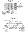
- the line imaging array of FIGURE 1 may be expanded to a two dimension infrared imaging array by placing a plurality of Line Imaging Arrays in parallel with each other as shown in FIGURE 5.
- the two dimension infrared imaging array comprises a plurality of Line Imaging Arrays identified as IDT-10 through IDT-19.
- Each of the Line Imaging Arrays IDT-10 through IDT-19 comprises a pair of interdigital tranducers, such as transducers 10 and 12 of FIGURE 1, which generate a pair of complementary surface acoustic wave trains which are 180° out of phase with each other as previously described.
- Associated with each line imaging array is a corresponding Interdigital Transducer designated IDT-20 through IDT-29 which individually corresponds to transducer 20 of FIGURE 1.
- Transducers IDT-20 through IDT-29 are connected to a Gate Circuit 30 which gates the outputs of Transducers IDT-20 through IDT-29, one at a time, to a Wave Train Detector 34 which performs the same function as Wave Train Detector 24 shown on FIGURE 1.
- the common connector electrodes of the plurality of Line Imaging Array IDT-10 through IDT-19 are connected in parallel to the output of an Impulse Generator 30.
- the output of Impulse Generator 30 is also connected to an Impulse Counter 36 which generates a number indicative of the number of impulses generated.
- a Decoder 38 responsive to the current number stored in Impulse Counter 36 produces an output signal which activates Gate 32 to transmit the wave trains generated by Transducers IDT-20 through IDT-29 one at a time to Wave Train Detector 34 in a predetermined sequence.
- This sequence may be a consecutive sequence or may be an interlaced sequence such as used in conventional cathode ray image tube (TV type) displays.
- the output signal indicative of the wave train from the last Transducer being transmitted to Detector 34 is also fed back to reset Impulse Counter 36 to begin a new gating sequence of the individual outputs from Transducers IDT-20 through IDT-29.
- interdigital transducer As previously described, only one of the two interdigital transducers of each Line Imaging Array is exposed to the infrared image, and this interdigital transducer may be coated with an infrared absorbing material to enhance its response to the infrared image as previously indicated.
- each Line Imaging Array produces two individual surface acoustic wave trains, such as wave trains 16 and 18 shown on FIGURE 1 which when transduced by Transducers IDT-20 to IDT-29 produce amplitude modulated wave trains which correspond to the intensity profile of the corresponding line segment of the infrared image.
- the first impulse signal is counted in Impulse Counter 36.
- the "I" count is decoded by Decoder 38 which generates a signal activating Gate 32 to transmit the wave train output of Transducer IDT-20 to Wave Train Detector 34 where it is converted to an analog or digital signal as required.
- the second impulse signal activates the Line Imaging Arrays IDT-10 through 19 to again produce wave trains which are detected by their respective Transducers IDT-20 through IDT-29.
- This second impulse signal indexes Impulse Counter 86 to the next higher number which is decoded by Decoder 38 to activate Gate 32 to transmit the amplitude modulated signal of a different Transducer to Wave Train Detector 34. If the predetermined readout sequence is sequential, then Gate 34 will transmit the output of Transducer IDT-21 to Wave Train Detector 34. However, if the predetermined sequence is interlaced, then Gate 34 will transmit the output of Transducer IDT-22 to Wave Train Detector 34.
- each Transducer IDT-20 through IDT-n may have its own Wave Train Detector 34 as shown on FIGURE 1. The output of these individual Wave Train Detectors may then be individually stored or sequentially gated to a utilization or storage device.
- FIGURE 6 shows the details of a Wave Train Detector 24 capable of generating a digital ontput indicative of the infrared line image.
- the Line Imaging Array 40 is the same as described with reference to FIGURE 1 receiving impulses from an Impulse Generator 26.
- the Impulse Generator 26 is triggered by a Square Wave Generator 42 generating square wave pulses at a frequency 2f.
- the output of the Square Wave Generator 42 is also received by a Phase Delay Circuit 44 and a Synchronous Chopper 46 illustrated as a sectored disc. Synchronous Chopper 46 chops the incoming infrared signal at a frequency "f" so that the incoming infrared signal modulates every other pair of surface acoustic wave trains generated by the Line Imaging Array 40.
- the Phase Delay Circuit 44 progressively delays the square wave signal and applies delayed square wave signal to an Amplitude Sample and Hold Circuit 48 and a Divide-by-Two (-2) Circuit 56.
- the two wave trains generated by the Line Imaging Array 40 are summed by interdigital Transducer 50 which corresponds to interdigital transducer 20 of FIGURE 1 and generates an amplitude modulated wave train as previously described.
- the amplitude modulated wave train is received by the Amplitude Sample and Hold Circuit 48 through diode 52.
- the Amplitude Sample and Hold Circuit 48 is triggered to sample and hold each wave in the amplitude modulated wave train, one at a time in a sequential order.
- the sequencing is achieved by gradually increasing the phase delay in Phase Delay Circuit 44.
- the Amplitude Sample and Hold Circuit 48 is triggered to sample in response to the leading edge of the delayed square wave received from Phase Delay Circuit 44.
- the output of the Amplitude Sample and Hold Circuit 48 is connected to a Lock-In Amplifier 54 which amplifies and temporarily stores the value of amplitude of the sampled wave in synchronization with the output of the Divide-by-Two Circuit 56.
- the output of the Lock-In Amplifier 54 is connected to an Analog-to-Digital Converter 58 which converts the amplitude of the sampled wave to a digital format.
- the Phase Delay Circuit 44 progressively delays the square wave generated by the Square Wave Generator 42 so that amplitude of each wave in the amplitude modulated wave train is sequentially sampled and converted to a digital format.
- the Phase Delay Circuit 44 thus enables one to scan detect each pixel element of the Line Array 40 in sequence across the line image.
- the output of the Divide-by-Two Circuit 56 is synchronized with the Chopper 46 so that the Lock-in Amplifier 54 looks at the difference between the amplitude of the wave generated for a given pixel element when exposed and not exposed to the infrared line image.
- the fixed pattern noise inherent in the Line Array 40 is thus eleminated.
- the Chopper 46, Divide-by-Two Circuit 56 and Lock-in Amplifier 54 may be eliminated and the A/D Converter 58 receives the output of the Sample and Hold Circuit 48.
Abstract
A surface acoustic wave infrared line imaging array having a first interdigital transducer (10) generating a first surface acoustic wave train (16) amplitude modulated by the temperature profile of the substrate (14) in response to a line segment of a received infrared image, a second interdigital transducer (12) generating a parallel reference surface acoustic wave train (18), equal in amplitude but 180° out of phase with said first surface acoustic wave train (16), and a third interdigital transducer (20) for summing the amplitudes of said first and reference surface acoustic wave trains (16, 18) to generate a wave train signal in which the individual waves are amplitude modulated in accordance with the intensity profile of the line segment of the infrared image received by the substrate (20) underlying the first interdigital transducer (10).
Description
- The invention is related to infrared image detectors and in particular to a surface acoustic wave (SAW) line imaging array.
- Infrared imaging detectors have a wide variety of commercial and military applications. Currently, most of infrared imaging detectors are self-scanned arrays of infrared semi-conductor detectors employing solid state charge transfer techniques. However, these self-scanned arrays are relatively expensive and require cryogenics which make them too bulky for many applications, such as intrusion alarms, infrared threat detectors and miniature infrared spectrometers. Pyroelectric imaging detectors operable at room temperature are slow, have poor sensitivity and respond only to time-varying signals. The invention is a monolithic, self-scanned infrared line imaging array which does not require cryogenic cooling, has a fast response, and is sensitive to stationary images.
- The surface acoustic wave infrared line imaging array comprises a first interdigital transducer receiving a line segment of an infrared image for generating a first surface acoustic wave train in response to an impulse signal, a second interdigital transducer, parallel to said first interdigital transducer for generating a second surface acoustic wave train, 180° out of phase with said first surface acoustic wave train, in response to said impulse signal, and a third interdigital transducer disposed proximate the ends of said first and second interdigital transducers for summing the amplitudes of said first and second surface acoustic wave trains to output a wave train signal in which the individual waves are amplitude modulated in accordance with the intensity or profile of the infrared image line segment received by the first interdigital transducer. The amplitude modulated wave train signal may be converted to an analog or digital format.
- One advantage of the surface acoustic wave infrared line imaging array is its small size and ease of manufacture. Another advantage is that it does not require cryogenic cooling and is operable at ambient temperatures. Another advantage is its fast response because the surface acoustic wave only samples the surface temperature of the substrate to a depth of only a few microns. These and other advantages will become more apparent from reading the specification in conjunction with the drawings.
-
- FIGURE 1 is perspective of the infrared line imaging array.
- FIGURE 2 is a graph showing the correlation between the intensity profile of the line segment of an infrared image and the corresponding temperature profile of the piezoelectric substrate.
- FIGURE 3 shows the amplitude modulated surface acoustic wave train resulting from the temperature profile of the substrate.
- FIGURE 4 shows the amplitude modulated wave train output from
interdigital transducer 20. - FIGURE 5 is a block diagram representation of a two-dimensional array of infrared line imaging arrays.
- FIGURE 6 is a block diagram of a detector generating digital information indicative of the intensity profile of the received infrared image.
- The invention is a surface acoustic wave (SAW) pyroelectric infrared line imaging array. Referring to FIGURE 1, the infrared line imaging array comprises a pair of side-by-side
interdigital transducers acoustic wave trains interdigital transducers acoustic waves - The
interdigital transducers piezoelectric substrate 14 such as zinc oxide (ZnO) lithium niobate (LiNb03) or any other temperature sensitive piezoelectric material as is known in the art. Thepiezoelectric substrate 14 may be a solid substrate as shown or alternatively be a piezoelectric layer disposed on a quartz or other crystalline substrate or glass. The structure of theinterdigital transducers common connector electrode 22 receiving the impulse signal or may be two independant interdigital transducers. The length of the interdigital transducers corresponds to the length of an infrared line image segment to be transduced and will have as many individual pairs of finger elements as required. Each pair of finger elements will constitute an individual pixel or picture element of the infrared line image. - The two independent surface
acoustic wave trains interdigital transducers interdigital transducer 20 disposed proximate the ends oftransducers Interdigital tranducer 20 responds to the two surfaceacoustic wave trains Detector 24 demodulates the resultant wave train output fromtransducer 20 and produces an output signal corresponding to the intensity profile of the received infrared line image. The signal fromDetector 20 may be converted into an analog or digital signal as required by a subsequent utilization device. - In operation, one of the
interdigital transducers piezoelectric substrate 14 underlying the one interdigital transducer will therefore have a temperature profile corresponding to the intensity profile of the linear infrared image as shown on FIGURE 2. - The surface acoustic wave generation efficiency, that is the electromechanical coupling coefficient between the finger elements of the interdigital transducer and the piezoelectric substrate is temperature dependent. For typical piezoelectric substrates, such as lithium niobate, the temperature dependent coupling coefficient is approximately 0.1 percent per degree centigrade (0.1$/oC). Therefore, the coupling coefficient of the individual finger pairs of the interdigital tranducers and the
piezoelectric substrate 14 will vary in accordance with the temperature profile of the substrate. Accordingly, the amplitudes of the individual waves of the generated wave train will be amplitude modulated in accordance with the temperature profile of the substrate as shown on FIGURE 3. - The surface temperature of the portion of the
piezoelectric substrate 14 underlying the other interdigital transducer is not exposed to the linear infrared image and its temperature profile will have a constant value. Therefore the amplitudes of the individual surface acoustic waves of the wave train generated by the other interdigital transducer will be equal. - As previously indicated,
interdigital transducers independent wave trains transducers interdigital transducer 20 in response to surfaceacoustic waves - However, when an infrared line image is incident on the surface of the
piezoelectric substrate 14 underlying only one of the interdigital transducers, for exampleinterdigital transducer 12, the portion of thepiezoelectric substrate 14underlying transducer 12 will be selectively heated. Since thepiezoelectric substrate 14 is a relatively poor thermal conductor, theportion underlying transducer 12 will assume a temperature profile corresponding to the intensity profile of the received infrared line image. This temperature profile will occur on the immediate surface of the piezoelectric substrate and have a depth of only a few microns. As a result, the coupling efficiency between the individual finger elements of theinterdigital transducer 12 and the substrate will vary along the length oftransducer 12 in accordance with the temperature profile of the underlying substrate. Accordingly, the amplitudes of the individual waves inwave train 18 generated bytransducer 12 will vary inversely to the temperature of the substrate underlying the respective finger elements oftransducer 12 as shown on FIGURE 3. In contrast, the amplitudes of the individual waves ofwave train 16 generated by transducer 10 being unaffected by the infrared line image incident ontranducer 12 will all have the same magnitude. - The result of the summation of the two
wave trains transducer 20 is no longer a null, but will be an amplitude modulated wave train having a frequency corresponding to the frequency ofwave trains transducer 20 are modulated according to the temperature profile of thesubstrate underlying transducer 12, which as previously indicated, corresponds to the intensity profile of the infrared line image. - The amplitude modulated wave train output from
transducer 20 may then be detected by Wave Train Detector 24 to produce either an analog signal whose amplitude varies in accordance with the intensity profile of the received infrared line image or may be converted byDetector 24 to digital information corresponding to the intensity profile of the infrared line image. The reading rate is determined by length of the line imaging array and the velocity of the surface acoustic wave which is approximately 0.3 centimeters per microsecond. - As is well known in the art, the section of the line imaging array receiving the infrared line image may be coated with an infrared absorbing material (not shown) to enhance the magnitude of the temperature profile of the substrate.
- It is recognized that the temperature profile of the substrate will also produce a corresponding phase shift in the surface acoustic wave train generated by the interdigital transducer receiving the infrared line image distorting the resultant wave train output from transducer 20. This distortion may be removed by dedicated electronics in the Wave
Train Detector 24 or may be subsequently removed by external processing using known techniques. - The line imaging array of FIGURE 1 may be expanded to a two dimension infrared imaging array by placing a plurality of Line Imaging Arrays in parallel with each other as shown in FIGURE 5. As shown in FIGURE 5 the two dimension infrared imaging array comprises a plurality of Line Imaging Arrays identified as IDT-10 through IDT-19. Each of the Line Imaging Arrays IDT-10 through IDT-19 comprises a pair of interdigital tranducers, such as
transducers - The outputs of Transducers IDT-20 through IDT-29 are connected to a
Gate Circuit 30 which gates the outputs of Transducers IDT-20 through IDT-29, one at a time, to aWave Train Detector 34 which performs the same function asWave Train Detector 24 shown on FIGURE 1. - The common connector electrodes of the plurality of Line Imaging Array IDT-10 through IDT-19 are connected in parallel to the output of an
Impulse Generator 30. The output ofImpulse Generator 30 is also connected to anImpulse Counter 36 which generates a number indicative of the number of impulses generated. A Decoder 38 responsive to the current number stored inImpulse Counter 36 produces an output signal which activatesGate 32 to transmit the wave trains generated by Transducers IDT-20 through IDT-29 one at a time toWave Train Detector 34 in a predetermined sequence. This sequence may be a consecutive sequence or may be an interlaced sequence such as used in conventional cathode ray image tube (TV type) displays. The output signal indicative of the wave train from the last Transducer being transmitted toDetector 34 is also fed back to reset Impulse Counter 36 to begin a new gating sequence of the individual outputs from Transducers IDT-20 through IDT-29. - As previously described, only one of the two interdigital transducers of each Line Imaging Array is exposed to the infrared image, and this interdigital transducer may be coated with an infrared absorbing material to enhance its response to the infrared image as previously indicated.
- In operation, the impulses to the common connector electrode of each Line Imaging Array are repetitively generated by the
Impulse Generator 30. Each Line Imaging Array produces two individual surface acoustic wave trains, such as wave trains 16 and 18 shown on FIGURE 1 which when transduced by Transducers IDT-20 to IDT-29 produce amplitude modulated wave trains which correspond to the intensity profile of the corresponding line segment of the infrared image. The first impulse signal is counted inImpulse Counter 36. The "I" count is decoded by Decoder 38 which generates asignal activating Gate 32 to transmit the wave train output of Transducer IDT-20 toWave Train Detector 34 where it is converted to an analog or digital signal as required. - The second impulse signal activates the Line Imaging Arrays IDT-10 through 19 to again produce wave trains which are detected by their respective Transducers IDT-20 through IDT-29. This second impulse signal indexes Impulse Counter 86 to the next higher number which is decoded by Decoder 38 to activate
Gate 32 to transmit the amplitude modulated signal of a different Transducer toWave Train Detector 34. If the predetermined readout sequence is sequential, thenGate 34 will transmit the output of Transducer IDT-21 toWave Train Detector 34. However, if the predetermined sequence is interlaced, thenGate 34 will transmit the output of Transducer IDT-22 toWave Train Detector 34. This procedure continues until outputs from all of the Transducers IDT-20 through IDT-29 have been transferred toWave Train Detector 34 in the predetermined sequence. The output signal of Decoder 38, indicative of the last wave train in the sequence being transmitted to theWave Train Detector 34, also is used to resetImpulse Counter 36 initializing it for the next sequence. - Those skilled in the art will recognize that the number of Line Imaging Arrays is not limited to the number of line arrays depicted in FIGURE 5, but may be fewer or as many as required for the particular application. Also, each Transducer IDT-20 through IDT-n may have its own
Wave Train Detector 34 as shown on FIGURE 1. The output of these individual Wave Train Detectors may then be individually stored or sequentially gated to a utilization or storage device. - The embodiment shown in FIGURE 6 shows the details of a
Wave Train Detector 24 capable of generating a digital ontput indicative of the infrared line image. TheLine Imaging Array 40 is the same as described with reference to FIGURE 1 receiving impulses from anImpulse Generator 26. TheImpulse Generator 26 is triggered by aSquare Wave Generator 42 generating square wave pulses at afrequency 2f. The output of theSquare Wave Generator 42 is also received by aPhase Delay Circuit 44 and aSynchronous Chopper 46 illustrated as a sectored disc.Synchronous Chopper 46 chops the incoming infrared signal at a frequency "f" so that the incoming infrared signal modulates every other pair of surface acoustic wave trains generated by theLine Imaging Array 40. ThePhase Delay Circuit 44 progressively delays the square wave signal and applies delayed square wave signal to an Amplitude Sample andHold Circuit 48 and a Divide-by-Two (-2)Circuit 56. - The two wave trains generated by the
Line Imaging Array 40 are summed byinterdigital Transducer 50 which corresponds tointerdigital transducer 20 of FIGURE 1 and generates an amplitude modulated wave train as previously described. The amplitude modulated wave train is received by the Amplitude Sample andHold Circuit 48 throughdiode 52. The Amplitude Sample andHold Circuit 48 is triggered to sample and hold each wave in the amplitude modulated wave train, one at a time in a sequential order. The sequencing is achieved by gradually increasing the phase delay inPhase Delay Circuit 44. The Amplitude Sample andHold Circuit 48 is triggered to sample in response to the leading edge of the delayed square wave received fromPhase Delay Circuit 44. - The output of the Amplitude Sample and
Hold Circuit 48 is connected to a Lock-In Amplifier 54 which amplifies and temporarily stores the value of amplitude of the sampled wave in synchronization with the output of the Divide-by-Two Circuit 56. The output of the Lock-In Amplifier 54 is connected to an Analog-to-Digital Converter 58 which converts the amplitude of the sampled wave to a digital format. As previously indicated, thePhase Delay Circuit 44 progressively delays the square wave generated by theSquare Wave Generator 42 so that amplitude of each wave in the amplitude modulated wave train is sequentially sampled and converted to a digital format. ThePhase Delay Circuit 44 thus enables one to scan detect each pixel element of theLine Array 40 in sequence across the line image. The output of the Divide-by-Two Circuit 56 is synchronized with theChopper 46 so that the Lock-inAmplifier 54 looks at the difference between the amplitude of the wave generated for a given pixel element when exposed and not exposed to the infrared line image. The fixed pattern noise inherent in theLine Array 40 is thus eleminated. When the fixed pattern noise is not a problem, theChopper 46, Divide-by-Two Circuit 56 and Lock-inAmplifier 54 may be eliminated and the A/D Converter 58 receives the output of the Sample andHold Circuit 48. - It is not intended that the invention be limited to the embodiments shown on the drawing and discussed in the specification. It is recognized that a person skilled in the art will be able to make changes or improvements to the line array infrared detector disclosed herein as set forth in the appended claims.
Claims (10)
1. A surface acoustic wave infrared line imaging array Characterized by:
a piezoelectric substrate (14) having a temperature dependent surface acoustic wave coupling efficiency;
impulse generator means (26) for generating an impulse signal:
first, interdigital transducer means (10) disposed on said piezoelectric substrate (14) for generating a first surface acoustic wave train (16) in response to said impulse signal;
second, interdigital transducer means (12) disposed on said piezoelectric substrate (14) for generating a second surface acoustic wave train (18) in response to said impulse signal, said second surface acoustic wave train having the same amplitude but being 180° out of phase with said first surface acoustic wave train (16);
third, interdigital transducer means (20) disposed on said piezoelectric substrate (14) for summing said first and second surface acoustic wave trains (16, 18) to generate an amplitude modulated wave train; and
means for isolating a received infrared image to illuminate one of said first and second interdigital transducer means (10, 12) to amplitude modulate the surface acoustic wave train (16, 18) generated by said one interdigital transducer means (10, 12);
2. The infrared line imaging array of Clafm 1 wherein said first and second interdigital transducer means (10, 12) have a common electrode (22) receiving said impulse signal.
3. The infrared line imaging array of Claim 2 wherein each of said first and second interdigital transducer means (10, 12) has a plurality of identical equally spaced finger pairs.
4. The infrared line imaging array of Claim 1 wherein said received infrared image illuminating said one interdigital transducer means (10, 12) has an intensity profile, said infrared line imaging array includes detector means (24) for generating an analog signal indicative of said intensity profile in response to said amplitude modulated wave train.
5. The infrared line imaging array of Claim 1 wherein said received infrared image illuminating said one interdigital transducer means (10, 12) has an intensity profile transducer means, said line imaging array further including detector means (24) for generating digital information indicative of said intensity profile in response to said amplitude modulated surface acoustic wave.
6. The infrared line imaging array of Claim 1 further including a plurality of said first, second and third interdigital transducer means (10, 12, 20) disposed parallel to each other.
7. The infrared line imaging array of Claim 6 further comprising:
detector means (34) for converting said amplitude modulated wave train to an analog signal; and
gate means (32) for transmitting said amplitude modulated wave trains generated by said plurality of third interdigital transducer means (20) to said detector means (34), one at a time, in a predetermined sequence in response to a signal indicative of said impulse signal.
8. The infrared line imaging array of Claim 6 further comprising:
detector means (34) for converting said amplitude modulated wave trains to digital information; and
gate means (32) for transmitting said amplitude modulated wave trains generated by said plurality of third interdigital transducer means (20) to said detector means (32), one at a time in a predetermined sequence in response to a signal indicative of said impulse signal.
9. A two dimensional imaging array for converting an infrared image to electrical signals having a plurality of surface acoustic wave line imaging arrays disposed in parallel relationship, each of said surface acoustic wave line imaging arrays generating an amplitude modulated wave train in response to an infrared image, and gate means connected to said plurality of surface acoustic line imaging arrays for outputting said plurality of amplitude modulated wave trains one at a time in a predetermined sequence, wherein each of said surface acoustic wave line imaging arrays is characterized by:
a first interdigital transducer (10) responsive to a line segment of said infrared image for generating a first surface acoustic wave train (16) in response to an impulse signal, said first acoustic wave train modulated in accordance with the intensity profile of said line segment of said infrared image;
a second interdigital transducer (12) parallel to said first interdigital transducer (10) for generating a second surface acoustic wave train (18) in response to said impulse signal, said second surface acoustic wave train (18) having an equal amplitude but 180° out of phase with said first surface acoustic wave train (16); and
a third interdigital transducer (20) disposed proximate the ends of said first and second interdigital tranducers (10, 12) for summing said first and second surface acoustic wave trains (16, 18) to generate said amplitude modulated wave train.
10. The two dimensional array of Claim 9 wherein said plurality of line imaging arrays are disposed on a common piezoelectric substrate (14) having a temperature dependent coupling efficiency.
Applications Claiming Priority (2)
| Application Number | Priority Date | Filing Date | Title |
|---|---|---|---|
| US614584 | 1984-05-29 | ||
| US06/614,584 US4584475A (en) | 1984-05-29 | 1984-05-29 | Surface acoustic wave infrared line imaging array |
Publications (2)
| Publication Number | Publication Date |
|---|---|
| EP0163060A2 true EP0163060A2 (en) | 1985-12-04 |
| EP0163060A3 EP0163060A3 (en) | 1988-07-27 |
Family
ID=24461894
Family Applications (1)
| Application Number | Title | Priority Date | Filing Date |
|---|---|---|---|
| EP85103995A Withdrawn EP0163060A3 (en) | 1984-05-29 | 1985-04-02 | Surface acoustic wave infrared line imaging array |
Country Status (4)
| Country | Link |
|---|---|
| US (1) | US4584475A (en) |
| EP (1) | EP0163060A3 (en) |
| JP (1) | JPS60257330A (en) |
| CA (1) | CA1242266A (en) |
Cited By (1)
| Publication number | Priority date | Publication date | Assignee | Title |
|---|---|---|---|---|
| CN114858285A (en) * | 2022-04-02 | 2022-08-05 | 电子科技大学 | Linear frequency modulation infrared nondestructive testing system |
Families Citing this family (7)
| Publication number | Priority date | Publication date | Assignee | Title |
|---|---|---|---|---|
| US5213105A (en) * | 1990-12-04 | 1993-05-25 | Research Corporation Technologies, Inc. | Frequency domain optical imaging using diffusion of intensity modulated radiation |
| JP3311869B2 (en) * | 1994-09-16 | 2002-08-05 | 株式会社東芝 | Semiconductor photoelectric conversion element and imaging device using the same |
| JP4769423B2 (en) * | 2004-03-10 | 2011-09-07 | ベックマン コールター, インコーポレイテッド | Liquid stirring device |
| US7786440B2 (en) * | 2007-09-13 | 2010-08-31 | Honeywell International Inc. | Nanowire multispectral imaging array |
| US9800805B2 (en) * | 2011-02-02 | 2017-10-24 | The Boeing Company | Frequency selective imaging system |
| KR102079659B1 (en) * | 2018-04-05 | 2020-02-20 | 해성디에스 주식회사 | Optical sensor device and Package including the same |
| CN111446329A (en) * | 2020-03-20 | 2020-07-24 | 苏州巧云信息科技有限公司 | Novel infrared detector and preparation method thereof |
Citations (3)
| Publication number | Priority date | Publication date | Assignee | Title |
|---|---|---|---|---|
| US4072863A (en) * | 1976-10-26 | 1978-02-07 | Roundy Carlos B | Pyroelectric infrared detection system |
| US4245330A (en) * | 1977-10-24 | 1981-01-13 | Rebourg Jean Claude | Elastic surface wave Hadamard transformer |
| JPS5950321A (en) * | 1982-09-16 | 1984-03-23 | Matsushita Electric Ind Co Ltd | Radiation thermometer |
Family Cites Families (1)
| Publication number | Priority date | Publication date | Assignee | Title |
|---|---|---|---|---|
| FR2483143B1 (en) * | 1980-05-20 | 1988-02-05 | Thomson Csf | ELASTIC WAVE PIEZOELECTRIC CONVOLVER DEVICE |
-
1984
- 1984-05-29 US US06/614,584 patent/US4584475A/en not_active Expired - Fee Related
-
1985
- 1985-04-02 EP EP85103995A patent/EP0163060A3/en not_active Withdrawn
- 1985-05-03 CA CA000480708A patent/CA1242266A/en not_active Expired
- 1985-05-24 JP JP60110585A patent/JPS60257330A/en active Pending
Patent Citations (3)
| Publication number | Priority date | Publication date | Assignee | Title |
|---|---|---|---|---|
| US4072863A (en) * | 1976-10-26 | 1978-02-07 | Roundy Carlos B | Pyroelectric infrared detection system |
| US4245330A (en) * | 1977-10-24 | 1981-01-13 | Rebourg Jean Claude | Elastic surface wave Hadamard transformer |
| JPS5950321A (en) * | 1982-09-16 | 1984-03-23 | Matsushita Electric Ind Co Ltd | Radiation thermometer |
Non-Patent Citations (2)
| Title |
|---|
| 18th ANNUAL PROCEEDINGS RELIABILITY PHYSICS 1980, Las Vegas, 8th-10th April 1980, pages 213-216, Institute of Electrical and Electronics Engineers, Inc., New York, US; D.E. ALLEN et al.: "A latent failure mechanism for surface acoustic wave components utilizing lithium niobate" * |
| PATENT ABSTRACTS OF JAPAN, vol. 8, no. 153 (P-287)[1590], 17th July 1984; & JP-A-59 050 321 (MATSUSHITA DENKI SANGYO K.K.) 23-03-84 * |
Cited By (1)
| Publication number | Priority date | Publication date | Assignee | Title |
|---|---|---|---|---|
| CN114858285A (en) * | 2022-04-02 | 2022-08-05 | 电子科技大学 | Linear frequency modulation infrared nondestructive testing system |
Also Published As
| Publication number | Publication date |
|---|---|
| CA1242266A (en) | 1988-09-20 |
| US4584475A (en) | 1986-04-22 |
| EP0163060A3 (en) | 1988-07-27 |
| JPS60257330A (en) | 1985-12-19 |
Similar Documents
| Publication | Publication Date | Title |
|---|---|---|
| CA2118597C (en) | Thin film pyroelectric imaging array | |
| CA1098615A (en) | Ferroelectric imaging system | |
| US4754139A (en) | Uncooled high resolution infrared imaging plane | |
| US4584475A (en) | Surface acoustic wave infrared line imaging array | |
| CA2044401A1 (en) | Multibeam optical and electromagnetic hemispherical/spherical sensor | |
| GB1501427A (en) | Electric image read-out device | |
| US4596930A (en) | Arrangement for multispectal imaging of objects, preferably targets | |
| US4873442A (en) | Method and apparatus for scanning thermal images | |
| US6204502B1 (en) | Heat radiation detection device and presence detection apparatus using same | |
| US3405271A (en) | Detector having radiation collector supported on electrically insulating thermally conducting film | |
| EP0368588A2 (en) | Pyroelectric infrared detector and manufacturing method of same | |
| US4737642A (en) | Arrangement for multispectral imaging of objects, preferably targets | |
| US4028548A (en) | IR imaging with surface wave readout | |
| GB1490739A (en) | System for reading acoustic images | |
| Porter et al. | Ferroelectric arrays: the route to low-cost uncooled infrared imaging | |
| US4837431A (en) | Variable phase time delay and signal aggregation system and method for achieving constant spatial resolution in scanning detection instruments | |
| JPH055291B2 (en) | ||
| US4100573A (en) | Thermal imaging transducer and system | |
| JPH0217988B2 (en) | ||
| GB1517902A (en) | Piezo-resistive device for the electrical read-out of an optical image | |
| Blackburn et al. | Pyroelectric detector arrays for thermal imaging | |
| Norkus et al. | Performance improvements for pyroelectric infrared detectors | |
| JP2000230858A (en) | Image pick-up element | |
| Kuwano et al. | The Pyroelectric Sensor | |
| JPH0731082B2 (en) | Array infrared detector |
Legal Events
| Date | Code | Title | Description |
|---|---|---|---|
| PUAI | Public reference made under article 153(3) epc to a published international application that has entered the european phase |
Free format text: ORIGINAL CODE: 0009012 |
|
| AK | Designated contracting states |
Designated state(s): DE FR GB |
|
| PUAL | Search report despatched |
Free format text: ORIGINAL CODE: 0009013 |
|
| AK | Designated contracting states |
Kind code of ref document: A3 Designated state(s): DE FR GB |
|
| STAA | Information on the status of an ep patent application or granted ep patent |
Free format text: STATUS: THE APPLICATION IS DEEMED TO BE WITHDRAWN |
|
| 18D | Application deemed to be withdrawn |
Effective date: 19890128 |
|
| RIN1 | Information on inventor provided before grant (corrected) |
Inventor name: LAO, BINNEG YANBING |