EP0159397B1 - Multistate optical switching and memory device using an organic charge transfer material - Google Patents
Multistate optical switching and memory device using an organic charge transfer material Download PDFInfo
- Publication number
- EP0159397B1 EP0159397B1 EP84113030A EP84113030A EP0159397B1 EP 0159397 B1 EP0159397 B1 EP 0159397B1 EP 84113030 A EP84113030 A EP 84113030A EP 84113030 A EP84113030 A EP 84113030A EP 0159397 B1 EP0159397 B1 EP 0159397B1
- Authority
- EP
- European Patent Office
- Prior art keywords
- optical
- organic
- state
- charge transfer
- electron acceptor
- Prior art date
- Legal status (The legal status is an assumption and is not a legal conclusion. Google has not performed a legal analysis and makes no representation as to the accuracy of the status listed.)
- Expired
Links
- 230000003287 optical effect Effects 0.000 title claims description 198
- 238000012546 transfer Methods 0.000 title claims description 102
- 239000000463 material Substances 0.000 title claims description 92
- PCCVSPMFGIFTHU-UHFFFAOYSA-N tetracyanoquinodimethane Chemical compound N#CC(C#N)=C1C=CC(=C(C#N)C#N)C=C1 PCCVSPMFGIFTHU-UHFFFAOYSA-N 0.000 claims description 93
- 150000003839 salts Chemical class 0.000 claims description 47
- 238000003860 storage Methods 0.000 claims description 37
- 238000013500 data storage Methods 0.000 claims description 34
- 150000001875 compounds Chemical class 0.000 claims description 31
- 230000003595 spectral effect Effects 0.000 claims description 27
- 238000001069 Raman spectroscopy Methods 0.000 claims description 26
- 230000003647 oxidation Effects 0.000 claims description 24
- 238000007254 oxidation reaction Methods 0.000 claims description 24
- 238000000034 method Methods 0.000 claims description 22
- -1 cyanomethylene functional group Chemical group 0.000 claims description 19
- 230000007935 neutral effect Effects 0.000 claims description 17
- 239000010949 copper Substances 0.000 claims description 14
- 150000005837 radical ions Chemical class 0.000 claims description 14
- RYGMFSIKBFXOCR-UHFFFAOYSA-N Copper Chemical compound [Cu] RYGMFSIKBFXOCR-UHFFFAOYSA-N 0.000 claims description 11
- 229910052802 copper Inorganic materials 0.000 claims description 11
- HZNVUJQVZSTENZ-UHFFFAOYSA-N 2,3-dichloro-5,6-dicyano-1,4-benzoquinone Chemical compound ClC1=C(Cl)C(=O)C(C#N)=C(C#N)C1=O HZNVUJQVZSTENZ-UHFFFAOYSA-N 0.000 claims description 10
- 230000008859 change Effects 0.000 claims description 10
- 238000006479 redox reaction Methods 0.000 claims description 10
- 238000006243 chemical reaction Methods 0.000 claims description 9
- 239000000203 mixture Substances 0.000 claims description 9
- 230000002441 reversible effect Effects 0.000 claims description 9
- 239000000126 substance Substances 0.000 claims description 7
- PXHVJJICTQNCMI-UHFFFAOYSA-N Nickel Chemical compound [Ni] PXHVJJICTQNCMI-UHFFFAOYSA-N 0.000 claims description 6
- 230000004044 response Effects 0.000 claims description 5
- 238000001228 spectrum Methods 0.000 claims description 5
- NLDYACGHTUPAQU-UHFFFAOYSA-N tetracyanoethylene Chemical group N#CC(C#N)=C(C#N)C#N NLDYACGHTUPAQU-UHFFFAOYSA-N 0.000 claims description 5
- JLTPSDHKZGWXTD-UHFFFAOYSA-N 2-[6-(dicyanomethylidene)naphthalen-2-ylidene]propanedinitrile Chemical compound N#CC(C#N)=C1C=CC2=CC(=C(C#N)C#N)C=CC2=C1 JLTPSDHKZGWXTD-UHFFFAOYSA-N 0.000 claims description 4
- XEEYBQQBJWHFJM-UHFFFAOYSA-N Iron Chemical compound [Fe] XEEYBQQBJWHFJM-UHFFFAOYSA-N 0.000 claims description 4
- 125000003118 aryl group Chemical group 0.000 claims description 4
- 238000010438 heat treatment Methods 0.000 claims description 4
- 239000011368 organic material Substances 0.000 claims description 4
- 229910052709 silver Inorganic materials 0.000 claims description 4
- 239000004332 silver Substances 0.000 claims description 4
- 239000011133 lead Substances 0.000 claims description 3
- 229910052759 nickel Inorganic materials 0.000 claims description 3
- NLPBZGOFTAIMRL-UHFFFAOYSA-N 2-[4-(dicyanomethylidene)-1,3-dithietan-2-ylidene]propanedinitrile Chemical compound N#CC(C#N)=C1SC(=C(C#N)C#N)S1 NLPBZGOFTAIMRL-UHFFFAOYSA-N 0.000 claims description 2
- MWIQXVQTLUPWDV-UHFFFAOYSA-N 4-thiopyran-4-ylidenethiopyran Chemical compound C1=CSC=CC1=C1C=CSC=C1 MWIQXVQTLUPWDV-UHFFFAOYSA-N 0.000 claims description 2
- VYZAMTAEIAYCRO-UHFFFAOYSA-N Chromium Chemical compound [Cr] VYZAMTAEIAYCRO-UHFFFAOYSA-N 0.000 claims description 2
- RWNKSTSCBHKHTB-UHFFFAOYSA-N Hexachloro-1,3-butadiene Chemical compound ClC(Cl)=C(Cl)C(Cl)=C(Cl)Cl RWNKSTSCBHKHTB-UHFFFAOYSA-N 0.000 claims description 2
- DGAQECJNVWCQMB-PUAWFVPOSA-M Ilexoside XXIX Chemical compound C[C@@H]1CC[C@@]2(CC[C@@]3(C(=CC[C@H]4[C@]3(CC[C@@H]5[C@@]4(CC[C@@H](C5(C)C)OS(=O)(=O)[O-])C)C)[C@@H]2[C@]1(C)O)C)C(=O)O[C@H]6[C@@H]([C@H]([C@@H]([C@H](O6)CO)O)O)O.[Na+] DGAQECJNVWCQMB-PUAWFVPOSA-M 0.000 claims description 2
- WHXSMMKQMYFTQS-UHFFFAOYSA-N Lithium Chemical compound [Li] WHXSMMKQMYFTQS-UHFFFAOYSA-N 0.000 claims description 2
- FYYHWMGAXLPEAU-UHFFFAOYSA-N Magnesium Chemical compound [Mg] FYYHWMGAXLPEAU-UHFFFAOYSA-N 0.000 claims description 2
- ZOKXTWBITQBERF-UHFFFAOYSA-N Molybdenum Chemical compound [Mo] ZOKXTWBITQBERF-UHFFFAOYSA-N 0.000 claims description 2
- ZLMJMSJWJFRBEC-UHFFFAOYSA-N Potassium Chemical compound [K] ZLMJMSJWJFRBEC-UHFFFAOYSA-N 0.000 claims description 2
- 229910052787 antimony Inorganic materials 0.000 claims description 2
- WATWJIUSRGPENY-UHFFFAOYSA-N antimony atom Chemical compound [Sb] WATWJIUSRGPENY-UHFFFAOYSA-N 0.000 claims description 2
- 150000004945 aromatic hydrocarbons Chemical class 0.000 claims description 2
- 229910000063 azene Inorganic materials 0.000 claims description 2
- 229910052788 barium Inorganic materials 0.000 claims description 2
- DSAJWYNOEDNPEQ-UHFFFAOYSA-N barium atom Chemical compound [Ba] DSAJWYNOEDNPEQ-UHFFFAOYSA-N 0.000 claims description 2
- 229910052792 caesium Inorganic materials 0.000 claims description 2
- TVFDJXOCXUVLDH-UHFFFAOYSA-N caesium atom Chemical compound [Cs] TVFDJXOCXUVLDH-UHFFFAOYSA-N 0.000 claims description 2
- 229910017052 cobalt Inorganic materials 0.000 claims description 2
- 239000010941 cobalt Substances 0.000 claims description 2
- GUTLYIVDDKVIGB-UHFFFAOYSA-N cobalt atom Chemical compound [Co] GUTLYIVDDKVIGB-UHFFFAOYSA-N 0.000 claims description 2
- 125000004122 cyclic group Chemical group 0.000 claims description 2
- 238000001514 detection method Methods 0.000 claims description 2
- 150000002390 heteroarenes Chemical class 0.000 claims description 2
- 229910052742 iron Inorganic materials 0.000 claims description 2
- 229910052744 lithium Inorganic materials 0.000 claims description 2
- 239000011777 magnesium Substances 0.000 claims description 2
- 229910052749 magnesium Inorganic materials 0.000 claims description 2
- 229910052750 molybdenum Inorganic materials 0.000 claims description 2
- 239000011733 molybdenum Substances 0.000 claims description 2
- 125000004433 nitrogen atom Chemical group N* 0.000 claims description 2
- 229910052700 potassium Inorganic materials 0.000 claims description 2
- 239000011591 potassium Substances 0.000 claims description 2
- 150000003254 radicals Chemical class 0.000 claims description 2
- MABNMNVCOAICNO-UHFFFAOYSA-N selenophene Chemical compound C=1C=C[se]C=1 MABNMNVCOAICNO-UHFFFAOYSA-N 0.000 claims description 2
- 229910052708 sodium Inorganic materials 0.000 claims description 2
- 239000011734 sodium Substances 0.000 claims description 2
- UGNWTBMOAKPKBL-UHFFFAOYSA-N tetrachloro-1,4-benzoquinone Chemical compound ClC1=C(Cl)C(=O)C(Cl)=C(Cl)C1=O UGNWTBMOAKPKBL-UHFFFAOYSA-N 0.000 claims description 2
- WFKWXMTUELFFGS-UHFFFAOYSA-N tungsten Chemical compound [W] WFKWXMTUELFFGS-UHFFFAOYSA-N 0.000 claims description 2
- 229910052721 tungsten Inorganic materials 0.000 claims description 2
- 239000010937 tungsten Substances 0.000 claims description 2
- 150000002894 organic compounds Chemical class 0.000 claims 11
- 230000015572 biosynthetic process Effects 0.000 claims 2
- 150000002500 ions Chemical class 0.000 claims 2
- VUMMZLLKRWNSJQ-UHFFFAOYSA-N 9-(2-thioxanthen-9-ylideneethylidene)thioxanthene Chemical compound C12=CC=CC=C2SC2=CC=CC=C2C1=CC=C1C2=CC=CC=C2SC2=CC=CC=C21 VUMMZLLKRWNSJQ-UHFFFAOYSA-N 0.000 claims 1
- 238000000862 absorption spectrum Methods 0.000 claims 1
- 125000002009 alkene group Chemical group 0.000 claims 1
- 125000006615 aromatic heterocyclic group Chemical group 0.000 claims 1
- 229910052804 chromium Inorganic materials 0.000 claims 1
- 239000011651 chromium Substances 0.000 claims 1
- 230000021615 conjugation Effects 0.000 claims 1
- 230000000977 initiatory effect Effects 0.000 claims 1
- 241000894007 species Species 0.000 description 65
- 239000000370 acceptor Substances 0.000 description 43
- 239000010408 film Substances 0.000 description 33
- 238000006276 transfer reaction Methods 0.000 description 13
- 230000002829 reductive effect Effects 0.000 description 11
- 230000005684 electric field Effects 0.000 description 8
- 229910052751 metal Inorganic materials 0.000 description 8
- 239000002184 metal Substances 0.000 description 8
- 230000008569 process Effects 0.000 description 7
- 239000010409 thin film Substances 0.000 description 7
- 238000003487 electrochemical reaction Methods 0.000 description 6
- 238000012306 spectroscopic technique Methods 0.000 description 6
- 230000005855 radiation Effects 0.000 description 5
- 230000027756 respiratory electron transport chain Effects 0.000 description 5
- 230000000694 effects Effects 0.000 description 4
- 238000004519 manufacturing process Methods 0.000 description 4
- BQCADISMDOOEFD-UHFFFAOYSA-N Silver Chemical compound [Ag] BQCADISMDOOEFD-UHFFFAOYSA-N 0.000 description 3
- 238000010521 absorption reaction Methods 0.000 description 3
- XKRFYHLGVUSROY-UHFFFAOYSA-N argon Substances [Ar] XKRFYHLGVUSROY-UHFFFAOYSA-N 0.000 description 3
- 230000005672 electromagnetic field Effects 0.000 description 3
- 230000009467 reduction Effects 0.000 description 3
- 239000007787 solid Substances 0.000 description 3
- 238000004833 X-ray photoelectron spectroscopy Methods 0.000 description 2
- 229910052786 argon Inorganic materials 0.000 description 2
- 230000001419 dependent effect Effects 0.000 description 2
- 238000010586 diagram Methods 0.000 description 2
- 238000005516 engineering process Methods 0.000 description 2
- 239000011888 foil Substances 0.000 description 2
- 230000006870 function Effects 0.000 description 2
- 150000002605 large molecules Chemical class 0.000 description 2
- 229920002521 macromolecule Polymers 0.000 description 2
- 230000007246 mechanism Effects 0.000 description 2
- 150000002739 metals Chemical class 0.000 description 2
- 229920000642 polymer Polymers 0.000 description 2
- 230000000007 visual effect Effects 0.000 description 2
- NRWXNYFTORBLPI-UHFFFAOYSA-N 1-(3,4-dihydrothiopyran-2-ylidene)-4H-thiopyran Chemical compound S1(C=CCC=C1)=C1SC=CCC1 NRWXNYFTORBLPI-UHFFFAOYSA-N 0.000 description 1
- JEXKJRQURAKWPN-UHFFFAOYSA-N 2-[5-(dicyanomethylidene)thiophen-2-ylidene]propanedinitrile Chemical compound N#CC(C#N)=C1C=CC(=C(C#N)C#N)S1 JEXKJRQURAKWPN-UHFFFAOYSA-N 0.000 description 1
- BSCHZGNYCFUYGZ-UHFFFAOYSA-N 9-(2-thioxanthen-9-ylideneethenylidene)thioxanthene Chemical compound C12=CC=CC=C2SC2=CC=CC=C2C1=C=C=C1C2=CC=CC=C2SC2=CC=CC=C21 BSCHZGNYCFUYGZ-UHFFFAOYSA-N 0.000 description 1
- WEVYAHXRMPXWCK-UHFFFAOYSA-N Acetonitrile Chemical compound CC#N WEVYAHXRMPXWCK-UHFFFAOYSA-N 0.000 description 1
- WKBOTKDWSSQWDR-UHFFFAOYSA-N Bromine atom Chemical group [Br] WKBOTKDWSSQWDR-UHFFFAOYSA-N 0.000 description 1
- NLZUEZXRPGMBCV-UHFFFAOYSA-N Butylhydroxytoluene Chemical compound CC1=CC(C(C)(C)C)=C(O)C(C(C)(C)C)=C1 NLZUEZXRPGMBCV-UHFFFAOYSA-N 0.000 description 1
- PXGOKWXKJXAPGV-UHFFFAOYSA-N Fluorine Chemical group FF PXGOKWXKJXAPGV-UHFFFAOYSA-N 0.000 description 1
- 238000001237 Raman spectrum Methods 0.000 description 1
- 238000000026 X-ray photoelectron spectrum Methods 0.000 description 1
- 230000009471 action Effects 0.000 description 1
- 150000001336 alkenes Chemical group 0.000 description 1
- 230000008901 benefit Effects 0.000 description 1
- GDTBXPJZTBHREO-UHFFFAOYSA-N bromine Chemical group BrBr GDTBXPJZTBHREO-UHFFFAOYSA-N 0.000 description 1
- 229910052794 bromium Inorganic materials 0.000 description 1
- 239000000460 chlorine Substances 0.000 description 1
- 229910052801 chlorine Inorganic materials 0.000 description 1
- 125000001309 chloro group Chemical group Cl* 0.000 description 1
- 239000000470 constituent Substances 0.000 description 1
- 239000013078 crystal Substances 0.000 description 1
- 230000018044 dehydration Effects 0.000 description 1
- 238000006297 dehydration reaction Methods 0.000 description 1
- 238000013461 design Methods 0.000 description 1
- 238000009792 diffusion process Methods 0.000 description 1
- HTXDPTMKBJXEOW-UHFFFAOYSA-N dioxoiridium Chemical compound O=[Ir]=O HTXDPTMKBJXEOW-UHFFFAOYSA-N 0.000 description 1
- 238000009826 distribution Methods 0.000 description 1
- 239000011737 fluorine Chemical group 0.000 description 1
- 229910052731 fluorine Inorganic materials 0.000 description 1
- 238000005286 illumination Methods 0.000 description 1
- 230000003993 interaction Effects 0.000 description 1
- 229910000457 iridium oxide Inorganic materials 0.000 description 1
- 238000005304 joining Methods 0.000 description 1
- 230000000670 limiting effect Effects 0.000 description 1
- 230000004807 localization Effects 0.000 description 1
- 238000002844 melting Methods 0.000 description 1
- 230000008018 melting Effects 0.000 description 1
- 125000000956 methoxy group Chemical group [H]C([H])([H])O* 0.000 description 1
- 125000002496 methyl group Chemical group [H]C([H])([H])* 0.000 description 1
- 230000004048 modification Effects 0.000 description 1
- 238000012986 modification Methods 0.000 description 1
- 230000005693 optoelectronics Effects 0.000 description 1
- JHRFTUUPRRIVKE-UHFFFAOYSA-N prop-1-ene-1,1,2,3,3-pentacarbonitrile Chemical compound N#CC(C#N)C(C#N)=C(C#N)C#N JHRFTUUPRRIVKE-UHFFFAOYSA-N 0.000 description 1
- 239000011253 protective coating Substances 0.000 description 1
- 125000002943 quinolinyl group Chemical group N1=C(C=CC2=CC=CC=C12)* 0.000 description 1
- 230000002468 redox effect Effects 0.000 description 1
- 238000011160 research Methods 0.000 description 1
- 230000000717 retained effect Effects 0.000 description 1
- 239000002904 solvent Substances 0.000 description 1
- 238000004611 spectroscopical analysis Methods 0.000 description 1
- 238000004544 sputter deposition Methods 0.000 description 1
- 239000011232 storage material Substances 0.000 description 1
- 125000001424 substituent group Chemical group 0.000 description 1
- 239000000758 substrate Substances 0.000 description 1
- 230000007704 transition Effects 0.000 description 1
- 238000001845 vibrational spectrum Methods 0.000 description 1
Images


Classifications
-
- G—PHYSICS
- G11—INFORMATION STORAGE
- G11C—STATIC STORES
- G11C13/00—Digital stores characterised by the use of storage elements not covered by groups G11C11/00, G11C23/00, or G11C25/00
- G11C13/0002—Digital stores characterised by the use of storage elements not covered by groups G11C11/00, G11C23/00, or G11C25/00 using resistive RAM [RRAM] elements
- G11C13/0009—RRAM elements whose operation depends upon chemical change
- G11C13/0014—RRAM elements whose operation depends upon chemical change comprising cells based on organic memory material
-
- B—PERFORMING OPERATIONS; TRANSPORTING
- B82—NANOTECHNOLOGY
- B82Y—SPECIFIC USES OR APPLICATIONS OF NANOSTRUCTURES; MEASUREMENT OR ANALYSIS OF NANOSTRUCTURES; MANUFACTURE OR TREATMENT OF NANOSTRUCTURES
- B82Y10/00—Nanotechnology for information processing, storage or transmission, e.g. quantum computing or single electron logic
-
- G—PHYSICS
- G03—PHOTOGRAPHY; CINEMATOGRAPHY; ANALOGOUS TECHNIQUES USING WAVES OTHER THAN OPTICAL WAVES; ELECTROGRAPHY; HOLOGRAPHY
- G03C—PHOTOSENSITIVE MATERIALS FOR PHOTOGRAPHIC PURPOSES; PHOTOGRAPHIC PROCESSES, e.g. CINE, X-RAY, COLOUR, STEREO-PHOTOGRAPHIC PROCESSES; AUXILIARY PROCESSES IN PHOTOGRAPHY
- G03C1/00—Photosensitive materials
- G03C1/72—Photosensitive compositions not covered by the groups G03C1/005 - G03C1/705
- G03C1/73—Photosensitive compositions not covered by the groups G03C1/005 - G03C1/705 containing organic compounds
-
- G—PHYSICS
- G11—INFORMATION STORAGE
- G11B—INFORMATION STORAGE BASED ON RELATIVE MOVEMENT BETWEEN RECORD CARRIER AND TRANSDUCER
- G11B7/00—Recording or reproducing by optical means, e.g. recording using a thermal beam of optical radiation by modifying optical properties or the physical structure, reproducing using an optical beam at lower power by sensing optical properties; Record carriers therefor
- G11B7/24—Record carriers characterised by shape, structure or physical properties, or by the selection of the material
- G11B7/241—Record carriers characterised by shape, structure or physical properties, or by the selection of the material characterised by the selection of the material
- G11B7/242—Record carriers characterised by shape, structure or physical properties, or by the selection of the material characterised by the selection of the material of recording layers
- G11B7/244—Record carriers characterised by shape, structure or physical properties, or by the selection of the material characterised by the selection of the material of recording layers comprising organic materials only
-
- G—PHYSICS
- G11—INFORMATION STORAGE
- G11C—STATIC STORES
- G11C11/00—Digital stores characterised by the use of particular electric or magnetic storage elements; Storage elements therefor
- G11C11/56—Digital stores characterised by the use of particular electric or magnetic storage elements; Storage elements therefor using storage elements with more than two stable states represented by steps, e.g. of voltage, current, phase, frequency
- G11C11/5664—Digital stores characterised by the use of particular electric or magnetic storage elements; Storage elements therefor using storage elements with more than two stable states represented by steps, e.g. of voltage, current, phase, frequency using organic memory material storage elements
-
- G—PHYSICS
- G11—INFORMATION STORAGE
- G11C—STATIC STORES
- G11C13/00—Digital stores characterised by the use of storage elements not covered by groups G11C11/00, G11C23/00, or G11C25/00
- G11C13/04—Digital stores characterised by the use of storage elements not covered by groups G11C11/00, G11C23/00, or G11C25/00 using optical elements ; using other beam accessed elements, e.g. electron or ion beam
-
- Y—GENERAL TAGGING OF NEW TECHNOLOGICAL DEVELOPMENTS; GENERAL TAGGING OF CROSS-SECTIONAL TECHNOLOGIES SPANNING OVER SEVERAL SECTIONS OF THE IPC; TECHNICAL SUBJECTS COVERED BY FORMER USPC CROSS-REFERENCE ART COLLECTIONS [XRACs] AND DIGESTS
- Y10—TECHNICAL SUBJECTS COVERED BY FORMER USPC
- Y10S—TECHNICAL SUBJECTS COVERED BY FORMER USPC CROSS-REFERENCE ART COLLECTIONS [XRACs] AND DIGESTS
- Y10S430/00—Radiation imagery chemistry: process, composition, or product thereof
- Y10S430/001—Electric or magnetic imagery, e.g., xerography, electrography, magnetography, etc. Process, composition, or product
- Y10S430/10—Donor-acceptor complex photoconductor
Definitions
- the present invention relates to a medium for optical switching and/or optical storage of information having at least one optically sensitive organic charge transfer (CT) compound having at least one electron donor moiety complexed with an organic electron acceptor moiety, which moieties undergo CT redox reactions in response to the application of electromagnetic energy at optical frequencies so as to switch from a first oxidation state to at least one second oxidation state, an apparatus containing such a medium and a method for optically storing information using said medium.
- CT organic charge transfer
- optical storage systems have one overriding disadvantage - prior art optical medium is not erasable.
- optical storage technology has found little application in computer technology, which requires both read, write and erase functions.
- the first state can be represented by a "0”
- the second switched state can be represented by to represent a "1”.
- That application also describes certain optical and thermal means for switching the organic material from the switch state ("1" state) back to the equilibrium state ("0" state).
- the organic optical devices described in that pending application are two-state systems which can only store two bits of information on a particular area of the organic optical storage medium.
- the present inventors have improved the organic charge transfer switching system described in U.S. patent 4,574,366 and have developed an organic storage medium which can optically store three or more bits of information at the same spot on the storage medium.
- the inventors have discovered that some amphoteric organic charge transfer materials can undergo multistage electron transfer reactions which enable the optical storage material to be switched among a plurality of states.
- each state can be uniquely identified by spectroscopic means and that energy from optical, infrared or thermal sources can be used to erase the storage medium and return it to its first or base state.
- the invented apparatus comprises: (1) an optical storage medium, generally in the form of a film of either a mixture of several charge transfer compounds of varying redox potential or of a single amphoteric organic charge transfer compound which is capable of undergoing a multistage charge transfer reaction; and (2) a source of applied optical energy which illuminates a spot on the optical storage medium and causes that spot to switch to one of a plurality of states.
- the organic material will switch from one state to another state as the applied optical field strength is increased.
- each state of said multistage electron transfer reaction can be identified by the presence of a unique set of redox species. Changes in the electronic or fundamental absorption modes are used to "read" the state of a "data storage spot" (i.e., each spot to be illuminated by the optical beam) on the optical storage medium by identifying the particular set of redox species present.
- an optical "write” beam can be used to switch the optical storage medium from the base state to one of three states, depending on the intensity of the optical field strength. Therefore, the optical "write” beam could be used to store multiple bits of data at each "data storage spot”. Similarly, optical and spectroscopic means can "read” the multiple bits of data stored at any "data storage spot” on the film. By appropriately placing the "data storage spots” on the optical storage medium, a conventional two dimensional configuration can be used to make an extremely dense optical storage device.
- thermal energy generated by an optical or thermal means
- the reverse multistage charge transfer reaction is a thermally activated process. If was also discovered that different organic charge transfer materials can be selected to produce either threshold or memory optical switching.
- the invented optical storage medium generally consists of a thin film of an amphoteric organic charge transfer material.
- the amphoteric organic charge transfer material is capable of undergoing a multistage charge transfer reaction. Each stage of said charge transfer reaction electrochemically generates multiple redox species. Each stage or state can be identified by observing the unique set of redox species generated.
- the amphoteric organic charge transfer material can be fabricated in several ways, which will be described in detail later in this specification. First, an amphoteric mixture can be produced by growing thin films containing a mixture of two different radical ion salts. Each radical ion salt, such as CuTCNQ or CuTCNQ(i-pri) 2 , exhibit separate bistate switching reactions.
- an amphoteric molecule can be complexed by chemically linking various acceptor molecules (such as TCNQ, TANP, or uTCNQ(i-pr) 2 together through sigma and pi bonding systems.
- acceptor molecules such as TCNQ, TANP, or uTCNQ(i-pr) 2
- highly delocalized radical ion acceptor molecules can be synthesized which exhibit the optical switching and amphoteric properties.
- an optical medium which can be optically switched from a equilibrium state to two or more switched states (redox states).
- the level of the electromagnetic field at optical frequencies determines into which state the optical medium is switched.
- the particular switched state can be subsequently identified by observing the changes in the electronic optical spectrum or the change in the fundamental absorption modes.
- the second object of the present invention is to produce an amphoteric organic charge medium which undergoes a multistage charge transfer reaction when subjected to an applied electric field. Electromagnetic energy at optical frequencies causes the material to undergo successive stages of a redox reaction as the optical field strength is increased. This stepwise switching allows an optical beam to switch the amphoteric organic charge transfer material from one stable oxidation state to a second, third, or fourth stable state. Each state can be identified by observing the optical characteristics of the redox species associated with that particular switched state.
- the amphoteric organic charge transfer material is "erasable" by applying thermal energy, which reverses the reaction and returns the material to its equilibrium state. Different amphoteric organic charge transfer materials can be selected to provide either memory or threshold multistate switching.
- a third object of the present invention is to use the amphoteric charge transfer material to produce a multistate optical storage device.
- An optical "write” beam is controlled to illuminate at least one "data storage spot" on the amphoteric film.
- the level of the applied electromagnetic field of the optical "write” beam is adjusted so that the illuminated "data storage spot” can be switched to a particular one of a plurality of states.
- Data from a "data storage spot” can be subsequently “read” by determining the optical characteristics of that "data storage spot” through spectroscopic techniques.
- the stored data can be “erased” by applying thermal energy to a particular part of the amphoteric organic charge transfer film, thereby returning that portion of the film to its base or equilibrium state.
- a medium for optical switching and/or optical storage of information having at least one optically sensitive organic charge transfer (CT) compound having at least one electron donor moiety complexed with an organic electron acceptor moiety, which moieties undergo CT redox reactions in response to the application of electromagnetic energy at optical frequencies so as to switch from a first oxidation state to at least one second oxidation state.
- CT optically sensitive organic charge transfer
- Equation (1) clearly shows a change in charge distribution as the organic salt switches from a first to a second state.
- the organic electron acceptor moiety In the first, or base state, the organic electron acceptor moiety is found almost exclusively in the reduced form (TCNQ). However, in the second, or switched state, the organic electron acceptor moiety is found in both its reduced (TCNQ') and neutral (TCNQ°) forms.
- each state is associated with a unique set of redox species.
- the acceptor moiety In the first state the acceptor moiety is found almost exclusively in the reduced form (e.g., only the TCNQ species is present); whereas, in the switched, or second state, the acceptor moiety exists in both the reduced and neutral form (e.g., TCNQ and TCNQ° redox species are present).
- Visual, spectroscopic, fluorescent and/or other optical means can be used to determine whether the bistate charge transfer salt is in the first or second state by identifying optical characteristics associated with each redox species.
- Figure 1 shows the Raman spectral bands for the organic charge transfer salt CuTCNQ:
- Figure 1 a shows the spectral bands for neutral TCNQ (e.g., TCNQ°);
- Figure 1b shows the spectral bands for CuTCNQ in the first state where essentially all the organic electron acceptor moiety is in a reduced form (e.g., only the TCNQ redox species is present);
- Figure 1 shows the spectral band for CuTCNQ in the second, or switch state, where the organic electron acceptor moiety is in both the reduced and neutral oxidation states (e.g., both the TCNQ and TCNQ° species are present).
- the Raman spectral bands are fundamental absorption modes which are sensitive to the oxidation state of the organic electron acceptor moiety, thereby uniquely identifying the redox species present (i.e., in our example, determining if the TCNQ or TCNQ° redox species are present).
- CuTCNQ is used as the organic charge transfer salt one need only analyze the 1451 cm- 1 spectral band to determine if the organic salt is in the first or second state. If the CuTCNQ organic charge transfer salt is in the first state, the spectral intensity is low at 1451 cm- 1 ; if the organic charge transfer salt is in the second state, the spectral intensity is high at 1451 cm- 1 .
- the first method of fabricating a multistate amphoteric charge transfer material is to produce a polycrystalline mixture from two bistate organic charge transfer salts. Under this method a film is grown containing two different radical ion salts mixed in a predetermined ratio. For example, neutral TCNQ° and neutral TCNQ(i-pr) 2 are added to a solvent such as CH 3 CN to form a solution. The solution is allowed to interact with a copper metal foil and corresponding complexes of Cu 2 (TCNQ:TCNQ(i-pr) 2 ] are grown on the metal foil producing a polycrystalline film. (It is to be understood that it is also within the contemplation of the invention to use other known methods to produce the polycrystalline mixture).
- Figure 2 is a Raman spectrophotometric plot illustrating each of the three states of Cu[TCNQ:TCNQ(i-pr) 21 .
- the copper TCNQ(i-pr) 2 stretching frequency is at 1390 cm- 1 which is shifted approximately 15 cm- 1 from the copper TCNQ stretching band at 1375 cm- 1.
- the Raman bands 10 identify the presence of the TCNQ and TCNQ(i-pr) 2 moieties in their reduced states (i.e., the TCNQ and redox species are present).
- Figure 2b shows the optical characteristics of the second state, which can be identified by the appearance of the Raman band 12 at 1451 cm -1 which is associated with the presence of the neutral redox species.
- an optical field strength had been applied to the film which was sufficient to switch the TCNQ(i-pr) 2 from its reduced species to its neutral species.
- the optical field strength was not sufficient to switch the TCNQ molecules.
- the second state can be identified by the presence of a new spectral peak at 1451 cm- 1 (element 12, Fig. 2b) corresponding to neutral species and a decrease in the intensity of fully charged TCNQ(i-pr) 2 species at 1462 cm- 1 .
- Figure 2c shows the film after the optical field intensity had been increased to a higher threshold level.
- the second optical field intensity now exceeds the threshold necessary to induce bistate switching in both CuTCNQ and CuTCNQ(i-pr) 2 salts.
- the resulting electrochemical charge transfer reaction now causes some of the CuTCNQ charge transfer complex to switch producing the neutral TCNQ° redox specie.
- the optical characteristics of the third state can be identified by the appearance of Raman band 14 at 1451 cm -1 which is associated with the present of the neutral TCNQ° redox species.
- Equation 2 describes the two state switching reaction of a CuTCNO(i-pr) 2 film when an optical beam having an intensity exceeding E l illuminates the film.
- the switched state can be uniquely identified by detecting the presence of both the and redox species.
- Equation 3 shows the two state switching reaction of a CuTCNQ film when an optical beam having an intensity exceeding E 2 illuminates the film.
- the switched state can be identified by the presence of both TCNQ° and TCNQ redox species.
- the switching optical threshold level for the two Equations is dependent upon the redox potential of the acceptor moiety.
- the table in Figure 3 shows the relationship between reduction potential of the acceptor moiety and the field strength switching threshold.
- a multistate amphoteric material can be fabricated from copper TCNQ and TCNQ(i-pr) 2 because the optical threshold to switch CuTCNQ is different from the optical threshold necessary to switch CuTCNQ(i-pr) 2 .
- such field strength dependence can be used to stepwise switch each bistable charge transfer salt thereby allowing the fabrication of a multistate amphoteric charge transfer medium.
- Equation 4 shows the switching characteristic of the amphoteric mixture Cu 2[ TCNQ:TCNQ(i-pr) 2] .
- the second state (state B) can be identified by detecting the redox species.
- the optical characteristics of the redox species can be identified by the Raman spectral band 12.
- the optical intensity equals or exceeds E 2
- the amphoteric material will be switched into the third state (state C).
- the third state is identified by detecting both the TCNQ° and the redox species.
- Such redox species can be detected by Raman spectroscopic means as shown in Figure 2c.
- Cu 2 [TCNQ:TCNQ(i-pr) 2 ] can be switched into three states: first, the amphoteric material will remain in the base state [state A] if the optical intensity is less than E,; secondly, the amphoteric material will be switched into the second state (state B) if the optical intensity exceeds E l but is less than E 2 ; and thirdly, the amphoteric material can be switched from the second state to the third state (state B to C) or from the base state to the third state (states A to B to C) when the optical intensity equals or exceeds E 2 .
- a spot on a Cu 2 [TCNQ:TCNQ(i-pr) 2 ] film can be switched into one of three states.
- the switched state of the Cu 2 [TCNQ:TCNQ(i-pr) 2 ] material can be reversed by using optical or thermal means to heat the material. It will be noted that Equation 4 is reversible and that the charge transfer reaction can be reversed, or the "memory erased" using thermal radiation to reform the original charge transfer complex [i.e., returning the amphoteric material to its base state].
- the Cu 2 [TCNQ:TCNQ(i-pr) 2 ] amphoteric material has been shown only as an example.
- Similar organic amphoteric materials can be formed from other complex mixtures of two or more charge transfer salts.
- two conditions must be met: (1) the two bistate charge transfer salts must switch at different optical intensity thresholds; and, (2) the redox species generated by the electrochemical reaction must have different electronic optical infrared and/or Raman spectral properties.
- TCNQ derivatives when complexed with a metal donor, will form an organic charge transfer salt capable of optical memory and/or switching. Examples of these TCNQ derivatives are shown in the following table:
- organic electron acceptor containing at least one cyanomethylene functional group is complexed with a donor moiety to form an organic salt, the organic salt will have memory and switching capabilities. Also Applicants have found that if an organic electron acceptor contains at least one quinoline unit is complexed with a donor moiety to form an organic salt, that organic salt will also have memory and switch capabilities.
- an organic salt is formed from the following organic electron acceptors, the organic salt will be capable of optical memory and/or switching: tetracyanoquinodimethane (TCNQ), tetracyanonaphthoquinodimethane (TNAP), tetracyanoethylene (TCNE), and 2,3-dichloro-5,6-dicyano-1,4-benzoquinone (DDQ), hexacyanobutylene (HCBD), and 11,11,12,12-tetracyano-1,4 naphthoquinodimethane (benzo-TCNQ), and 2,5-bis (dicyanomethylene)-2,5-dihydrothiophene, and 2,5-bis (dicyanomethylene)-2,5-selenophene, and thiophene-(T)-TCNQ, and (selenophene (Se)-TCNQ) and tetracyano-quinoquinazolinoquinazoline (TCNQ),
- the organic salt will switch optically: copper, silver, lead, nickel, lithium, sodium, potassium, barium, chrome, molybdenum, tungsten, cobalt, iron, antimony, cesium and magnesium.
- the following organic substances can also act as donors, and if complexed with an organic electron acceptor to form an organic salt, the organic salt will be capable of optical memory and/or switching: tetrathioethylenes, dithiodaminoethylenes, dithiodisalino ethylelenes, tetraminoethylenes, azenes, and aromatic hydrocarbons.
- organic transfer salts formed with organic electron acceptors having either cyanomethylene functional groups or quinolene units and other organic salts having similar characteristics may be found with switch from the above-referenced first state to second state in the presence of optical radiation.
- the bistate optical switching compounds can be combined as taught by the present invention to produce a multistate amphoteric organic charge transfer medium.
- the switched states for such amphoteric organic charge transfer material can be distinguished because Raman modes of neutral and radical ion species are strongly affected by substitute groups attached to the quinoid structure.
- Optical properties associated with different redox species can be identified by a variety of different techniques. In general, spectroscopic means can be used to determine the particular state of a location on a multistate amphoteric charge transfer medium. Both infrared spectroscopic means and Raman spectroscopic means can be used to identify the particular switched state.
- Raman spectroscopic techniques or similar techniques which analyzes a particular narrow band of laser light reflected from the multistate amphoteric organic charge transfer medium
- any other well known spectroscopic or similar technique can be used which has the capability of identifying a change in oxidation state of the organic electron acceptor moiety or change in the reduction state of the donor moiety (i.e., X-ray photoelectron spectroscopy (XPS), Raman or infrared spectroscopic means can detect the change in oxidation state of the donor and/or the organic electron acceptor moiety).
- XPS X-ray photoelectron spectroscopy
- the redox species characteristic of a particular switch state can be identified by visual color changes in the material.
- the table in Figure 4 outlines some of the observed color changes in bistate material which can be mixed to form multistate material.
- some of the organic acceptor molecules such as TCNQ(OMe) z , TCNO[Oi-pr][OM e ]) and TCNQ (i-pr) 2 exhibit a broad band fluorescence in the oxidized state but not in the reduced state.
- This fluorescence shown in Figure 5, can be used to record the change in oxidation state and to separate the different redox species from one another for certain materials in this case TCNQ[(OMe)(Oi-pr)] (e.g., the presence of fluorescence may indicate that a particular neutral redox species is present). Therefore, multistate amphoteric charge transfer materials can be produced from two different bistate radical ion salts. Such multiswitching can be made from a variety of related radical ion acceptor molecules. Some examples of such acceptor molecules are listed above and shown in Figure 6. The multiswitching effect can be observed in these acceptors by mixing different molecules together or by changing the donor metal.
- a multistate amphoteric organic charge transfer material made from a film composed of CuTCNQ and AgTCNQ will switch at different applied optical fields.
- the optical field intensity at which a constituent bistate charge transfer salt switches is dependent upon the strength of the donor-acceptor bond.
- An alternative method for producing a multistate amphoteric charge transfer material is to chemically link various acceptor molecules together with through sigma and pi bonding systems to produce a large molecule.
- the large molecule produced is amphoteric and can be switched optically into several states with each state identifiable by a unique set of redox species. This method guarantees that the acceptor molecules will react with the metal donor equally to form a molecular multiswitching system.
- Figure 7 shows several examples of two linked radical ion acceptor molecules. It will be noted that many known chemical linking chains can be used other than those illustrated in Figure 7.
- the two chemically linking molecules shown in Figure 7, connect the TCNQ moiety with a TCNQ moiety having substitute R groups such as chlorine, bromine, fluorine, CH 3 , OMe or other similar substituent groups.
- R groups such as chlorine, bromine, fluorine, CH 3 , OMe or other similar substituent groups.
- Equation (5) describes the multistate switching reaction for a (TCNQ)-CH 2 SCH 2 COCH 2 SCH 2 -(TNAP) amphoteric charge transfer molecule:
- the material When the optical intensity is increased and is equal to or greater than E 2 the material will be switched from the second state to the third state (state B to C) or from the initial or base state to the third state (state A to B to C).
- the [(TCNQ°) ⁇ R ⁇ (TNAP°)], and [(TCNQ O )-R-(TNAP*)] redox species are present in the third state.
- Optical or spectroscopic means discussed earlier in this specification, can identify the third state by detecting the presence of the [(TCNO°)R(TNAP°)] redox species.
- the bistate organic charge transfer salts which are linked to form the amphoteric material must: (1) switch from their base state to a switched state at different applied fields at optical frequencies: and, (2) the redox species generated by the multistep redox reaction must have features easily identifiable by optical/spectroscopic means.
- two or more bistate organic charge transfer salt molecules or two or more multistate molecular compounds can be chemically linked to form a large molecular complex which can be optically switched into four or more states.
- Equation (5) represents a reversible reaction and that thermal energy generated by optical or thermal means can return part or all of the amphoteric material to the base state. By this process, information stored on such an amphoteric charge transfer medium can be "erased”.
- the aforementioned concepts can be utilized to synthesize and develop large delocalized molecular systems which exhibit amphoteric redox properties in additional to the optically induced charged transfer properties associated with the TCNQ class of organic materials.
- the synthesized molecule must undergo an optically induced redox process and transfer electrons inter or intramolecular without rupturing electron pair sigma bonds;
- each radical partner in the molecular system must exhibit independent thermal stability;
- the optically induced electrochemical reaction which generates various redox species could be reversible; and, (4) the redox species must be readily identifiable using optical or other spectroscopic techniques.
- the sensitized molecules combine the multistate redox feature found in many known amphoteric molecules with the optical properties associated with the switching effect observed in copper and silver TCNQ type complexes.
- Examples of strongly delocalized radical ion acceptor molecules which exhibit the multiswitching effect are shown in Figure 8.
- Several of these amphoteric molecules (15,16) are derivatives of the TCNE radical ion with inserted alkene or aromatic groups (i.e., 2,3-dichloro-5,6-dicyano-1,4-benzoquinone and p-chloranil).
- FIG. 8 illustrates one of a class of delocalized molecules (19) composed of tetracyanoarenoquinodimethane with an extended pi-system; and, a compound (20) having alternate forms 1,3-squaric acid diamides; and, two compounds (21, 22) composed of dicyanomethylidene substituted with quinocyclopropenes.
- amphoteric donor molecules complexed with radical ion electron acceptors will exhibit the optically induced multiswitching phenomena.
- the acceptor compounds can be complexed with various metals such as copper, lead, nickel and silver.
- the multistate amphoteric charge transfer molecular compounds are grown as thin films or as single crystals which can be fabricated into various device geometries.
- Equation (6) describes the multistate switching reaction in the material formed from Cu 2 [C 10 N 6 ], an amphoteric charge transfer molecules: where E Z >E 1
- the amphoteric material When the Cu 2 [C 10 N 6 ] material is illuminated by an optical beam having a field intensity equal to or greater than E 1 but less than E 2 , the amphoteric material will switch from the initial or base state (State A) into the second state (State B). As shown in Equation (6), the and redox species are present in the second state. Optical and spectroscopic means discussed earlier in this specification, can identify the second state by detecting the presence of these redox species. When the optical intensity is increased and is equal to or greater than E 2 the material will be switched from the second state to the third state (State B to State C) or from the base state to the third state (State A to B to C).
- the Cu + 2 (C 10 N 6 ] -2 , and Cu + [C 10 N 6 ] o 2 redox species are present in the third state.
- Optical/spectroscopic means discussed earlier in the specification, can identify the third state by detecting the presence of the Cu°[C 10 N 6 ] o 2 redox specie.
- Cu 2 [C 10 N 6 ] -2 molecular structure was shown in the above example, it is understood that other amphoteric molecular structures described earlier in Figures 8 and 9, or similar compounds, can form synthesized molecular complexes which exhibit optical multistate switching. It is also contemplated that such multistate synthetic molecules can be fabricated which have four or more switching states in accordance with the present invention.
- Equation (6) represents a reversible electron transfer reaction and thermal energy generated by optical or thermal means can return all or part of the amphoteric material to the initial state. By this process, the memory medium formed from such synthetic amphoteric molecules can be "erased”.
- FIG. 10 graphically illustrates the generalized optical switching characteristics.
- the organic switching medium is composed of redox species identified as "B" in Figure 10.
- An optical "write” beam is used to switch a spot on the material into a switched state (such spot referred as a "data storage spot”). If the optical intensity of the "write" beam exceeds an intensity threshold T i , but is less than threshold T 2 , the illuminated spot will jump to the second state.
- the second state can be identified by the appearance of a new redox specie identified by A 1 in Figure 10.
- Figure 11 is a truth table for such a generalized amphoteric system.
- the table shows that by identifying the presence of certain redox species, the state of the "data storage spot" can be determined. For example, if the A4 redox species is detected by optical means, it indicates that the "data storage spot" is in state 4. If, the A3 species is detected but not significant amounts of the A4 redox species, we are in the third state. If the A 2 species is detected but not significant amounts of the A3 and A4 redox species, we are in the second state. If, however, the A 2 , A3 and A4 species are not significantly detected the "data storage spot" is in the first or base state.
- the switching phenomenon observed in such amphoteric charge transfer material can be either threshold switching or memory switching.
- threshold switching the illuminated spot rapidly returns to the base state after the optical beam is removed.
- memory switching the illuminated spot requires additional energy to return to the lower thermodynamically stable state after the beam is removed. In most cases, ambient thermal energy is insufficient to rapidly reverse the electrochemical reaction back to the lower state (e.g., thermodynamically more stable state).
- the length of time memory can be retained depends on: (1) the particular material, (2) the diameter of the "write” beam; (3) the duration and intensity of the "write” beam; and (4) the thickness of amphoteric charge transfer film.
- incident optical energy necessary to switch the amphoteric charge transfer material from one state to another depends on several factors including: (1) bonding energy; (2) size of the illumination "write” beam; (3) the duration of the optical "write” beam, and (4) the thickness or geometric arrangement of the amphoteric film or material.
- the frequency of the optical beam can be chosen from the ultraviolet, visible, and/or infrared regions of the electromagnetic spectrum.
- FIG. 12 is a schematic diagram of an optical storage system using such a multistate amphoteric charge transfer material as the optical storage medium.
- the amphoteric charge transfer material 29 is deposited on or in a supporting base material 31.
- the amphoteric material can be grown on a metal donor base material 31, as described earlier in the specification, or other methods such as sputtering can deposit the amphoteric material 29 on the base material 31.
- An optional transparent protective coating 33 may be deposited on the surface of the amphoteric material film 29.
- An optical "write" beam 35 is focused on a specific spot 37 on the surface of the amphoteric material 29.
- the optical "write” beam can be a high intensity light source or laser source such as an Argon or C0 2 laser focused to generate a field on the film surface in the area of the "data storage spot".
- the optical "write” beam has several discrete intensity levels, each intensity level causing the "data storage spot” to switch into a particular state.
- the intensity of the beam will cause the "data storage spot” to switch states - for example, in a three-state optical medium where the optical beam intensity is at the first threshold (T,) the "data storage spot” will switch from the base state to the second state; at intensity T 2 the "data storage spot” will be switched to the third state; and, at an intensity of T 3 the "data storage spot” will be switched into the fourth state.
- T first threshold
- T 2 the optical intensity necessary to produce the above state changes depends on the choice of the amphoteric material, the film thickness or geometry and the area and intensity of the optical "write" beam.
- an optical "write” 35 can be directed by known optical or electrical control means to other "data" storage spot" locations on the surface of the amphoteric charge transfer material 29 and can switch such other locations from the base state to one of several switch states. By controlling the beam intensity at a specific "data storage spot" location, multiple bits of data can be stored at that location in the optical storage medium.
- an optical "write” beam can be used to switch the optical storage medium through the base state to one of three states depending on the intensity of the optical field strength. Therefore, the "write” beam could be used to store a three-bit data code at each "data storage spot". If the memory apparatus were used in conjunction with a binary computer, the first or base state could be represented by "01", the second switched state could be represented by a "10"; and, the third switched state could be represented by a "11 ". Alternatively, the memory apparatus could be used in connection with a base three computing system.
- FIG. 13 is a schematic of the spectroscopic means and shows “data storage spot” localizations 37 and 39, which are two of a possible plurality of storage locations containing data.
- a light source, or “reading” optical beam 41 is directed to illuminate one of the locations 37 with an intensity well below the first intensity threshold, so that the state at location 28 is not disturbed.
- the light source 41, for Raman spectroscopic analysis could be a monochromatic source and Applicants suggest the use of a laser source.
- Reflected and/or emitted light 43 from the selected location on the film surface 37 is collected and filtered by the optical band pass filter 45 allowing reflected light to pass through an optical means 47 for measuring the spectral intensity of each desired band.
- the optical means looks at the magnitude of particular spectral bands (Raman bands) which identify a particular redox species. (It would be possible to have a plurality of filter/detector combinations to measure the magnitude of reflected light in each band of interest. Alternatively, traditional Raman spectroscopic means could be utilized.) Based on the magnitude of the spectral intensity in each selected band, logic detection circuitry 48, of known design, determines the set of redox species present, which in turn uniquely defines the switched state of that "data storage spot".
- the "reading" optical beam 41 can be directed by well known optical means to each of the plurality of "data storage spot" locations (e.g., 37, 38) on the surface of the amphoteric organic charge transfer material 29 to determine the state of each particular location. That is to say, for an amphoteric charge transfer material having three states, the spectroscopic means will determine the state of a particular "data storage spot” and thereby determine the three-bit word stored at that "data storage spot".
- Figure 14 is a schematic drawing showing the thermal erase means which is used to reverse the electrochemical charge transfer reaction and cause at least one of a plurality of "data storage spot" locations on the surface of the amphoteric organic charge transfer material 29 to return to the base state.
- Figure 14 shows two alternative embodiments for the thermal erase means.
- the first embodiment uses thermal radiation from an optical beam 49 focused on the location 37 to generate sufficient heat to switch the area back to the base state. Applicants have found that the C0 2 laser, with an intensity below the first threshold, can be focused on location 37 for a time period long enough to generate sufficient thermal energy to switch the location back to the base state, or more thermodynamically stable state.
- the optical heating beam 40 can be directed by a well known optical means to erase other locations on the amphoteric organic charge transfer material surface 29.
- An alternative embodiment uses an electrical heating element 51, located below substrate 31, to generate sufficient thermal energy to "erase” a portion of the amphoteric charge transfer material film 29.
- the optical write beam 35, optical read beam 41, and the optical heating beam 49 can be generated by a single laser source by varying the intensity and duration of the illuminating beam. It is within the contemplation of the Applicants that other well known means can be used to generate the desired optical "write/read” and “erase” beams, and to direct such beams to the desired location on the amphoteric organic charge transfer material surface.
Landscapes
- Engineering & Computer Science (AREA)
- Chemical & Material Sciences (AREA)
- Nanotechnology (AREA)
- Physics & Mathematics (AREA)
- General Physics & Mathematics (AREA)
- Computer Hardware Design (AREA)
- Mathematical Physics (AREA)
- Theoretical Computer Science (AREA)
- Crystallography & Structural Chemistry (AREA)
- Materials Engineering (AREA)
- Optical Record Carriers And Manufacture Thereof (AREA)
- Non-Silver Salt Photosensitive Materials And Non-Silver Salt Photography (AREA)
- Thermal Transfer Or Thermal Recording In General (AREA)
- Optical Recording Or Reproduction (AREA)
- Optical Modulation, Optical Deflection, Nonlinear Optics, Optical Demodulation, Optical Logic Elements (AREA)
Description
- The present invention relates to a medium for optical switching and/or optical storage of information having at least one optically sensitive organic charge transfer (CT) compound having at least one electron donor moiety complexed with an organic electron acceptor moiety, which moieties undergo CT redox reactions in response to the application of electromagnetic energy at optical frequencies so as to switch from a first oxidation state to at least one second oxidation state, an apparatus containing such a medium and a method for optically storing information using said medium.
- 2. Description of the Contemporary and/or Prior Art
- With the advent of the information revolution, recent research activities have focused on developing optical storage systems and optoelectronic switches. The interaction of laser light with matter has been intensely investigated because of its use in optical memory systems. Potentially, optical recording can produce information storage densities in excess of 100 million bits per square centimeter. Currently many optical memory devices rely on crystalline phase transitions (J. Stuke, Journal of Non-Crystalline Solids, Vol. 4, (1970)) or on photochemical hole burning (PHB) in which a laser pits the material in an effort to store data. An article entitled "Laser Marking of a Thin Organic Film" by J. J. Wrobel et al, Applied Physics Letter 40, (11) 1 June 1982, describes such a technique using a laser beam to burn holes in a thin organic film. Similarly, optical writing on blue sputtered iridium oxide films is reported by Mabosch et al in Applied Physics Letter 41 (1), 1 July 1982. This technique uses an optical writing mechanism to thermally induce dehydration at temperatures below the melting point of the optical medium. An article entitled "Light- induced Phenomena in Dye-polymer Systems" by V. Novotny et al, The Journal ofApplied Physics 50 (3), March 1979, describes an optical marking process based on diffusion in a dye-polymer system.
- The prior art optical storage systems have one overriding disadvantage - prior art optical medium is not erasable. As a result, optical storage technology has found little application in computer technology, which requires both read, write and erase functions.
- U.S. patent 4,371,883 (entitled "Current Controlled Bistate Electrical Organic Thin Film Switching Device (TCNQ)", filed March 14, 1980) and U.S. Patent 4,507,672 (entitled "Method of Fabricating a Current Controlled Bistate Electrical Organic Thin Film Switching Device (TCNQ)", filed June 7, 1982) filed by Richard S. Potember, Theodore O. Poehler and Dwaine O. Cowan, disclose a class of organic charge transfer salts, such as CuTCNQ, which exhibit stable and reproducible bistate switching between an equilibrium, or first state, and a second state, in the presence of an applied electrical field. These references disclose that certain organic charge transfer salts will undergo a bistate reversible electrochemical topotactic redox reaction in the presence of an applied electric field. The electrical field causes the organic salt to switch from a first state to a second (i.e., bistate switching). A detectable impedance change occurs between the equilibrium, or first state, and the second state thereby allowing one to determine if a particular area is in the first or second state. In specific, an electrical field is applied across a thin film of CuTCNQ, or an equivalent organic charge transfer salt. When the applied electrical field exceeds a threshold value the impedance across the thin organic film will drop from a relatively high impedance to a relatively low impedance.
- Two papers written by Richard S. Potember et al report that when the organic film is electrically switched, the second state has different optical properties from the equilibrium or first state: (1) "The Vibrational and X-ray Photoelectron Spectra of Semiconducting Copper-TCNQ Films" Chemica Scripta, Vol. 17, 219-221 (1981); and (2) "Electrical Switching and Memory Phenomena in Semiconducting Organic Thin Films" American Chemical Society Symposium Series No. 184 (1982). These articles describe infrared spectroscopic means and reference well known Raman spectroscopic techniques (S. Matsuzaki et al, "Raman Spectra of Conducting TCNQ Salts" Solid State Communications, Vol. 33, pp. 403-405, 1980) for determining if the CuTCNQ film, switched by an AC or DC electric field is in the first or second state. Follow-up work reported by E. I. Kamitsos et al used Raman spectroscopic techniques to verify the electrochemical charge transfer equation described in the above-referenced articles which causes the CuTCNQ salt to switch from the first to second state: "Raman Study of the Mechanism of Electrical Switching in CuTCNQ films" Solid State Communications, Vol. 42, No. 8, pp. 561-565 (1982). These papers point out that spectroscopic means can be used to discern whether an area of CuTCNQ switched by an applied electrical field is in the first or second state.
- Potember and Poehler, the present inventors, with Benson, in U.S. patent 4,574,366 entitled "Optical Storage and Switching Devices Using Organic Charge Transfer Salts", Serial No. 464,771, filed February 7, 1983, disclose a bistate optical switching device. They discovered that certain organic charge transfer salts will also experience two-state switching when exposed to optical radiation. It was discovered that when the optical radiation exceeds a certain threshold, the organic charge transfer salt switched from a first to a second state. Spectroscopic and other optical means are used to determine if a portion of the organic charge transfer material was in the first, equilibrium, or second switch state. That pending U.S. application describes certain optical devices used to store binary information - the first state can be represented by a "0", and the second switched state can be represented by to represent a "1". That application also describes certain optical and thermal means for switching the organic material from the switch state ("1" state) back to the equilibrium state ("0" state). However, the organic optical devices described in that pending application are two-state systems which can only store two bits of information on a particular area of the organic optical storage medium.
- The present inventors have improved the organic charge transfer switching system described in U.S. patent 4,574,366 and have developed an organic storage medium which can optically store three or more bits of information at the same spot on the storage medium. The inventors have discovered that some amphoteric organic charge transfer materials can undergo multistage electron transfer reactions which enable the optical storage material to be switched among a plurality of states. The inventors have further discovered that each state can be uniquely identified by spectroscopic means and that energy from optical, infrared or thermal sources can be used to erase the storage medium and return it to its first or base state.
- The invented apparatus comprises: (1) an optical storage medium, generally in the form of a film of either a mixture of several charge transfer compounds of varying redox potential or of a single amphoteric organic charge transfer compound which is capable of undergoing a multistage charge transfer reaction; and (2) a source of applied optical energy which illuminates a spot on the optical storage medium and causes that spot to switch to one of a plurality of states. The organic material will switch from one state to another state as the applied optical field strength is increased.
- The inventors have discovered that at particular optical field strengths, the amphoteric medium will switch into a particular state. The inventors have also discovered that each state of said multistage electron transfer reaction, can be identified by the presence of a unique set of redox species. Changes in the electronic or fundamental absorption modes are used to "read" the state of a "data storage spot" (i.e., each spot to be illuminated by the optical beam) on the optical storage medium by identifying the particular set of redox species present.
- For example, with an amphoteric organic charge transfer material having a 4-stage electron transfer reaction, an optical "write" beam can be used to switch the optical storage medium from the base state to one of three states, depending on the intensity of the optical field strength. Therefore, the optical "write" beam could be used to store multiple bits of data at each "data storage spot". Similarly, optical and spectroscopic means can "read" the multiple bits of data stored at any "data storage spot" on the film. By appropriately placing the "data storage spots" on the optical storage medium, a conventional two dimensional configuration can be used to make an extremely dense optical storage device.
- The inventors also discovered that thermal energy (generated by an optical or thermal means) can be used to "erase" all or part of the optical storage film and return each state of the multiple storage spot to its base or equilibrium state. The reverse multistage charge transfer reaction is a thermally activated process. If was also discovered that different organic charge transfer materials can be selected to produce either threshold or memory optical switching.
- The invented optical storage medium generally consists of a thin film of an amphoteric organic charge transfer material. The amphoteric organic charge transfer material is capable of undergoing a multistage charge transfer reaction. Each stage of said charge transfer reaction electrochemically generates multiple redox species. Each stage or state can be identified by observing the unique set of redox species generated. The amphoteric organic charge transfer material can be fabricated in several ways, which will be described in detail later in this specification. First, an amphoteric mixture can be produced by growing thin films containing a mixture of two different radical ion salts. Each radical ion salt, such as CuTCNQ or CuTCNQ(i-pri)2, exhibit separate bistate switching reactions. Secondly, an amphoteric molecule can be complexed by chemically linking various acceptor molecules (such as TCNQ, TANP, or uTCNQ(i-pr)2 together through sigma and pi bonding systems. Third, highly delocalized radical ion acceptor molecules can be synthesized which exhibit the optical switching and amphoteric properties.
- Accordingly, it is one object of the present invention to provide an optical medium which can be optically switched from a equilibrium state to two or more switched states (redox states). The level of the electromagnetic field at optical frequencies determines into which state the optical medium is switched. Further, the particular switched state can be subsequently identified by observing the changes in the electronic optical spectrum or the change in the fundamental absorption modes.
- The second object of the present invention is to produce an amphoteric organic charge medium which undergoes a multistage charge transfer reaction when subjected to an applied electric field. Electromagnetic energy at optical frequencies causes the material to undergo successive stages of a redox reaction as the optical field strength is increased. This stepwise switching allows an optical beam to switch the amphoteric organic charge transfer material from one stable oxidation state to a second, third, or fourth stable state. Each state can be identified by observing the optical characteristics of the redox species associated with that particular switched state. The amphoteric organic charge transfer material is "erasable" by applying thermal energy, which reverses the reaction and returns the material to its equilibrium state. Different amphoteric organic charge transfer materials can be selected to provide either memory or threshold multistate switching.
- A third object of the present invention is to use the amphoteric charge transfer material to produce a multistate optical storage device. An optical "write" beam is controlled to illuminate at least one "data storage spot" on the amphoteric film. The level of the applied electromagnetic field of the optical "write" beam is adjusted so that the illuminated "data storage spot" can be switched to a particular one of a plurality of states. Data from a "data storage spot" can be subsequently "read" by determining the optical characteristics of that "data storage spot" through spectroscopic techniques. The stored data can be "erased" by applying thermal energy to a particular part of the amphoteric organic charge transfer film, thereby returning that portion of the film to its base or equilibrium state.
- These objects are achieved by a medium for optical switching and/or optical storage of information having at least one optically sensitive organic charge transfer (CT) compound having at least one electron donor moiety complexed with an organic electron acceptor moiety, which moieties undergo CT redox reactions in response to the application of electromagnetic energy at optical frequencies so as to switch from a first oxidation state to at least one second oxidation state.
- According to the invention the medium is characterized in that it comprises:
- a) a mixture of at least two CT compounds having different CT redox potentials and/or
- b) at least one CT compound wherein the
- i) electron acceptor moiety and/or
- ii) electron donor moiety has at least two structurally different regions with different redox potentials, and that the different redox reactions occur independently of each other at field strength values unique to each compound or region and that each particular oxidation state has an identifiably different optical spectrum.
- While several features of the present invention relate to optical storage medium and optical memory devices, it is to be understood that the above-mentioned multistate switching function of the amphoteric organic charge transfer material can have application in other optical devices and optically sensitive apparatus. The above-mentioned objectives, as well as other objectives and advantages of the present invention, will become readily apparent after reading the ensuing description of several non-limiting illustrative embodiments and viewing the accompanying drawings.
- In order that the present invention may be more fully understood, it will now be described, by way of example, with reference to the following drawings in which:
- Figure 1 is a graph of the Raman spectral bands for bistate CuTCNQ; Figure 1a shows the spectral bands for neutral TCNQ; Figure 1 b shows the spectral bands for CuTCNQ in the first state; Figure 1 c shows the spectral bands for CuTCNQ in the switched state;
- Figure 2 is a Raman spectrophotometric plot illustrating each of the three switched states of Cu[TCNQ (i-pr)2]; Figure 2a shows the optical characteristics of the base state; Figure 2b shows the optical characteristics of the second state; Figure 2c shows the optical characteristics of the third state;
- Figure 3 is a table showing the relationship between reduction potential of the acceptor moiety and the field strength switching threshold;
- Figure 4 is a table which outlines some of the observed visible color changes in bistate material which can be mixed to form multistate material;
- Figure 5 is a graph showing the fluorescence of TCNQ[(OMe)(O-i-pr)] in its neutral state;
- Figure 6 shows molecular drawings of radical ion acceptor molecules which can be used to make multistate switching material in accordance with the present invention;
- Figure 7 shows several examples of two chemically linked radical ion acceptor molecules which exhibit multistate optical switching;
- Figure 8 shows several highly delocalized radical ion acceptor molecules which exhibit multistate switching as taught by the present invention;
- Figure 9 shows several highly delocalized radical ion donor molecules which exhibit multistate switching as taught by the present invention;
- Figure 10 graphically illustrates the generalized optical switching characteristics of multistate amphoteric charge transfer material as taught by the present invention;
- Figure 11 is a truth table illustrating the generalized optical switching characteristics of multistate amphoteric charge transfer material as taught by the present invention;
- Figure 12 is a schematic diagram of an optical storage system using such multistate amphoteric charge transfer material as taught by the present invention;
- Figure 13 is a schematic representation of the optical means used to evaluate the state of each "data storage spot"; and,
- Figure 14 is a schematic drawing showing the thermal erasure means.
- To understand multistage switching it is necessary to understand some of the principles of bistate optical switching as described in WO-A-84/08169 corresponding to the co-pending U.S. application entitled "Optical Storage and Switching Devices using Optical Charge Transfer Salts" (SN 464,771) which is incorporated herein by reference. The basic electrochemical topotactic redox reaction which occurs when a bistable organic charge transfer salt, such as CuTCNQ, is illuminated with a beam having sufficient optical field strength and switched from a first to a second state, is shown below:

- It is believed that switching occurs because the optical beam (i.e., an electromagnetic field at optical frequencies) causes the bonds between the organic electron acceptor (in this case TCNQ) and the donor (represented by M) to break, allowing a charge to transfer from the donor to the organic electron acceptor. The foregoing Equation (1) clearly shows a change in charge distribution as the organic salt switches from a first to a second state. In the first, or base state, the organic electron acceptor moiety is found almost exclusively in the reduced form (TCNQ). However, in the second, or switched state, the organic electron acceptor moiety is found in both its reduced (TCNQ') and neutral (TCNQ°) forms.
- It will be noted from Equation (1) that each state is associated with a unique set of redox species. In the first state the acceptor moiety is found almost exclusively in the reduced form (e.g., only the TCNQ species is present); whereas, in the switched, or second state, the acceptor moiety exists in both the reduced and neutral form (e.g., TCNQ and TCNQ° redox species are present). Visual, spectroscopic, fluorescent and/or other optical means can be used to determine whether the bistate charge transfer salt is in the first or second state by identifying optical characteristics associated with each redox species. Figure 1 shows the Raman spectral bands for the organic charge transfer salt CuTCNQ: Figure 1 a shows the spectral bands for neutral TCNQ (e.g., TCNQ°); Figure 1b shows the spectral bands for CuTCNQ in the first state where essentially all the organic electron acceptor moiety is in a reduced form (e.g., only the TCNQ redox species is present); Figure 1 shows the spectral band for CuTCNQ in the second, or switch state, where the organic electron acceptor moiety is in both the reduced and neutral oxidation states (e.g., both the TCNQ and TCNQ° species are present). The Raman spectral bands are fundamental absorption modes which are sensitive to the oxidation state of the organic electron acceptor moiety, thereby uniquely identifying the redox species present (i.e., in our example, determining if the TCNQ or TCNQ° redox species are present). When CuTCNQ is used as the organic charge transfer salt one need only analyze the 1451 cm-1 spectral band to determine if the organic salt is in the first or second state. If the CuTCNQ organic charge transfer salt is in the first state, the spectral intensity is low at 1451 cm-1; if the organic charge transfer salt is in the second state, the spectral intensity is high at 1451 cm-1.
- The first method of fabricating a multistate amphoteric charge transfer material, as taught by the present invention, is to produce a polycrystalline mixture from two bistate organic charge transfer salts. Under this method a film is grown containing two different radical ion salts mixed in a predetermined ratio. For example, neutral TCNQ° and neutral TCNQ(i-pr)2 are added to a solvent such as CH3CN to form a solution. The solution is allowed to interact with a copper metal foil and corresponding complexes of Cu2(TCNQ:TCNQ(i-pr)2] are grown on the metal foil producing a polycrystalline film. (It is to be understood that it is also within the contemplation of the invention to use other known methods to produce the polycrystalline mixture).
- When Cu2[uTCNQ:TCNQ(i-pr)2], an amphoteric charge transfer material, is irradiated by an optical source (such as an Argon ion laser) the optical characteristics of the material change with increases in the optical power density (watts/cm2). Three different optical spectra were observed which correspond to three switched states. Three switched states were noted because the optical field strength required to switch CuTCNQ from its base state to its second state is higher than the optical energy necessary to switch CuTCNQ(i-pr)2. The Applicants were able to use such field strength dependence to stepwise switch each copper bistable salt from its base state to its switch state at a different optical field strengths.
- Figure 2 is a Raman spectrophotometric plot illustrating each of the three states of Cu[TCNQ:TCNQ(i-pr)21. Figure 2a shows the optical characteristics of the unswitched or base state. In the base state, strong v4(C=C stretching)
Raman bands 10 were observed for both copper TCNQ and copper TCNO(i-pr)2. The copper TCNQ(i-pr)2 stretching frequency is at 1390 cm-1 which is shifted approximately 15 cm-1 from the copper TCNQ stretching band at 1375 cm-1. TheRaman bands 10 identify the presence of the TCNQ and TCNQ(i-pr)2 moieties in their reduced states (i.e., the TCNQ and
Raman band 12 at 1451 cm-1 which is associated with the presence of the neutral
element 12, Fig. 2b) corresponding to neutral
- Figure 2c shows the film after the optical field intensity had been increased to a higher threshold level. The second optical field intensity now exceeds the threshold necessary to induce bistate switching in both CuTCNQ and CuTCNQ(i-pr)2 salts. The resulting electrochemical charge transfer reaction now causes some of the CuTCNQ charge transfer complex to switch producing the neutral TCNQ° redox specie. The optical characteristics of the third state can be identified by the appearance of Raman band 14 at 1451 cm-1 which is associated with the present of the neutral TCNQ° redox species.
- The multistate switching observed in Cu2[TCNQ:TCNQ(i-pr)2] might best be understood in view of Equations 2-4 following:


-
Equation 2 describes the two state switching reaction of a CuTCNO(i-pr)2 film when an optical beam having an intensity exceeding El illuminates the film. In this electrochemical reaction the switched state can be uniquely identified by detecting the presence of both the

- Equation 4 shows the switching characteristic of the amphoteric mixture Cu2[TCNQ:TCNQ(i-pr)2]. It will be noted that the amphoteric film is switched to the second state (state B) after the film has been illuminated with an optical field intensity greater than E, but less than E2. The second state (state B) can be identified by detecting the


spectral band 12. When the optical intensity equals or exceeds E2 the amphoteric material will be switched into the third state (state C). The third state is identified by detecting both the TCNQ° and the
- Therefore, Cu2[TCNQ:TCNQ(i-pr)2] can be switched into three states: first, the amphoteric material will remain in the base state [state A] if the optical intensity is less than E,; secondly, the amphoteric material will be switched into the second state (state B) if the optical intensity exceeds El but is less than E2; and thirdly, the amphoteric material can be switched from the second state to the third state (state B to C) or from the base state to the third state (states A to B to C) when the optical intensity equals or exceeds E2. Therefore, by adjusting the intensity of the incident optical beam a spot on a Cu2[TCNQ:TCNQ(i-pr)2] film can be switched into one of three states. The switched state of the Cu2[TCNQ:TCNQ(i-pr)2] material can be reversed by using optical or thermal means to heat the material. It will be noted that Equation 4 is reversible and that the charge transfer reaction can be reversed, or the "memory erased" using thermal radiation to reform the original charge transfer complex [i.e., returning the amphoteric material to its base state]. The Cu2[TCNQ:TCNQ(i-pr)2] amphoteric material has been shown only as an example. Similar organic amphoteric materials can be formed from other complex mixtures of two or more charge transfer salts. In order to produce such an amphoteric organic charge transfer material two conditions must be met: (1) the two bistate charge transfer salts must switch at different optical intensity thresholds; and, (2) the redox species generated by the electrochemical reaction must have different electronic optical infrared and/or Raman spectral properties.
- Applicants have discovered a number of organic charge transfer compound which will undergo bistate optical switching as above-described, in the present of energy from an optical field. Applicants have found that various TCNQ derivatives, when complexed with a metal donor, will form an organic charge transfer salt capable of optical memory and/or switching. Examples of these TCNQ derivatives are shown in the following table:

- Applicants have further found that if an organic electron acceptor containing at least one cyanomethylene functional group is complexed with a donor moiety to form an organic salt, the organic salt will have memory and switching capabilities. Also Applicants have found that if an organic electron acceptor contains at least one quinoline unit is complexed with a donor moiety to form an organic salt, that organic salt will also have memory and switch capabilities. In specific, if an organic salt is formed from the following organic electron acceptors, the organic salt will be capable of optical memory and/or switching: tetracyanoquinodimethane (TCNQ), tetracyanonaphthoquinodimethane (TNAP), tetracyanoethylene (TCNE), and 2,3-dichloro-5,6-dicyano-1,4-benzoquinone (DDQ), hexacyanobutylene (HCBD), and 11,11,12,12-tetracyano-1,4 naphthoquinodimethane (benzo-TCNQ), and 2,5-bis (dicyanomethylene)-2,5-dihydrothiophene, and 2,5-bis (dicyanomethylene)-2,5-selenophene, and thiophene-(T)-TCNQ, and (selenophene (Se)-TCNQ) and tetracyano-quinoquinazolinoquinazoline (TCQQ) and hexacyano- trimethylenecyclopropane (HMCTMCP) and 2,4-bis (dicyanomethylene)-1,3-dithietan (BDDT), and any of the TCNQ derivatives shown in the above table.
- Applicants have discovered that if the following metals are complexed with the above-referenced organic electron acceptor to form an organic salt, the organic salt will switch optically: copper, silver, lead, nickel, lithium, sodium, potassium, barium, chrome, molybdenum, tungsten, cobalt, iron, antimony, cesium and magnesium. In addition, the following organic substances can also act as donors, and if complexed with an organic electron acceptor to form an organic salt, the organic salt will be capable of optical memory and/or switching: tetrathioethylenes, dithiodaminoethylenes, dithiodisalino ethylelenes, tetraminoethylenes, azenes, and aromatic hydrocarbons. It is to be understood that other organic transfer salts formed with organic electron acceptors having either cyanomethylene functional groups or quinolene units and other organic salts having similar characteristics, may be found with switch from the above-referenced first state to second state in the presence of optical radiation. The bistate optical switching compounds can be combined as taught by the present invention to produce a multistate amphoteric organic charge transfer medium.
- The switched states for such amphoteric organic charge transfer material can be distinguished because Raman modes of neutral and radical ion species are strongly affected by substitute groups attached to the quinoid structure. Optical properties associated with different redox species can be identified by a variety of different techniques. In general, spectroscopic means can be used to determine the particular state of a location on a multistate amphoteric charge transfer medium. Both infrared spectroscopic means and Raman spectroscopic means can be used to identify the particular switched state. Although Applicants' prefer to use Raman spectroscopic techniques, or similar techniques which analyzes a particular narrow band of laser light reflected from the multistate amphoteric organic charge transfer medium, it is to be understood that any other well known spectroscopic or similar technique can be used which has the capability of identifying a change in oxidation state of the organic electron acceptor moiety or change in the reduction state of the donor moiety (i.e., X-ray photoelectron spectroscopy (XPS), Raman or infrared spectroscopic means can detect the change in oxidation state of the donor and/or the organic electron acceptor moiety).
- In certain cases the redox species characteristic of a particular switch state can be identified by visual color changes in the material. The table in Figure 4 outlines some of the observed color changes in bistate material which can be mixed to form multistate material. In addition, some of the organic acceptor molecules such as TCNQ(OMe)z, TCNO[Oi-pr][OMe]) and TCNQ (i-pr)2 exhibit a broad band fluorescence in the oxidized state but not in the reduced state. This fluorescence, shown in Figure 5, can be used to record the change in oxidation state and to separate the different redox species from one another for certain materials in this case TCNQ[(OMe)(Oi-pr)] (e.g., the presence of fluorescence may indicate that a particular neutral redox species is present). Therefore, multistate amphoteric charge transfer materials can be produced from two different bistate radical ion salts. Such multiswitching can be made from a variety of related radical ion acceptor molecules. Some examples of such acceptor molecules are listed above and shown in Figure 6. The multiswitching effect can be observed in these acceptors by mixing different molecules together or by changing the donor metal. For example, a multistate amphoteric organic charge transfer material made from a film composed of CuTCNQ and AgTCNQ will switch at different applied optical fields. The optical field intensity at which a constituent bistate charge transfer salt switches is dependent upon the strength of the donor-acceptor bond.
- It is also contemplated by the inventors that three or more bistate organic charge transfer salts can be combined as taught herein to form an amphoteric charge transfer material which will exhibit four or more switching states.
- An alternative method for producing a multistate amphoteric charge transfer material is to chemically link various acceptor molecules together with through sigma and pi bonding systems to produce a large molecule. The large molecule produced is amphoteric and can be switched optically into several states with each state identifiable by a unique set of redox species. This method guarantees that the acceptor molecules will react with the metal donor equally to form a molecular multiswitching system. Figure 7 shows several examples of two linked radical ion acceptor molecules. It will be noted that many known chemical linking chains can be used other than those illustrated in Figure 7. The two chemically linking molecules shown in Figure 7, connect the TCNQ moiety with a TCNQ moiety having substitute R groups such as chlorine, bromine, fluorine, CH3, OMe or other similar substituent groups. It will be noted that during the electrochemical switching reaction the covalent bonds between the linking chain and the TCNQ moiety and the linking chain and the TCNQ derivative moiety do not break. It will also be noted that Raman spectroscopic modes for the redox species are strongly affected by such substitute groups attached to the quinoid structure - thus allowing various redox species formed during the electrochemical reaction to be easily identified using optical and spectroscopic techniques.
- Equation (5) describes the multistate switching reaction for a (TCNQ)-CH2SCH2COCH2SCH2-(TNAP) amphoteric charge transfer molecule:

- When the (TCNQ)-R-(TNAP) amphoteric charge transfer material, where R represents the ―CH2SCH2COCH2SCH― chemical linking chain, is illuminated by an optical beam having an intensity equal to or greater than El but less than E2, the material will switch from the base state (state A) into the second state (state B). As shown in Equation (5) the


- Although the [(TCNQ)-R-(TNAP)] compound has been used to describe the amphoteric material formed by a chemically linking process, it is to be understood that other bistate organic charge transfer salt can be joined by equivalent chemical chains to form amphoteric molecules. The molecules diagrammed in Figure 7 as well as the bistate switching compounds mentioned earlier in this application can be chemically linked to form amphoteric compounds which will exhibit multistate optical switching. It is within the contemplation of the inventors to claim chemically-linked amphoteric materials generated by linking bistate organic transfer salts. The only limitation being that the bistate organic charge transfer salts, which are linked to form the amphoteric material must: (1) switch from their base state to a switched state at different applied fields at optical frequencies: and, (2) the redox species generated by the multistep redox reaction must have features easily identifiable by optical/spectroscopic means.
- It is also contemplated by the inventors that two or more bistate organic charge transfer salt molecules or two or more multistate molecular compounds can be chemically linked to form a large molecular complex which can be optically switched into four or more states.
- It must also be noted that Equation (5) represents a reversible reaction and that thermal energy generated by optical or thermal means can return part or all of the amphoteric material to the base state. By this process, information stored on such an amphoteric charge transfer medium can be "erased".
- The aforementioned concepts can be utilized to synthesize and develop large delocalized molecular systems which exhibit amphoteric redox properties in additional to the optically induced charged transfer properties associated with the TCNQ class of organic materials. Several important factors must be met to accomplish this end: (1) the synthesized molecule must undergo an optically induced redox process and transfer electrons inter or intramolecular without rupturing electron pair sigma bonds; (2) each radical partner in the molecular system must exhibit independent thermal stability; (3) the optically induced electrochemical reaction which generates various redox species could be reversible; and, (4) the redox species must be readily identifiable using optical or other spectroscopic techniques. In essence, the sensitized molecules combine the multistate redox feature found in many known amphoteric molecules with the optical properties associated with the switching effect observed in copper and silver TCNQ type complexes. Examples of strongly delocalized radical ion acceptor molecules which exhibit the multiswitching effect are shown in Figure 8. Several of these amphoteric molecules (15,16) are derivatives of the TCNE radical ion with inserted alkene or aromatic groups (i.e., 2,3-dichloro-5,6-dicyano-1,4-benzoquinone and p-chloranil). Other molecules shown in Figure 8 (17, 18) are two-stage radical ions in which the end groups form part of a cyclic pi-system with exhibited aromatic characteristics in the oxidized state (i.e. pentacyanopropene and 2-dicyanomethylene-1,1,2,2 tetracyanopropanediide). In addition, Fig. 8 illustrates one of a class of delocalized molecules (19) composed of tetracyanoarenoquinodimethane with an extended pi-system; and, a compound (20) having
alternate forms 1,3-squaric acid diamides; and, two compounds (21, 22) composed of dicyanomethylidene substituted with quinocyclopropenes. In addition to acceptor type amphoteric molecules, amphoteric donor molecules complexed with radical ion electron acceptors will exhibit the optically induced multiswitching phenomena. Figure 9 shows several such amphoteric donor molecules including compound (23) benzotrithiophene; compound (24) heteroarenes with bridgehead nitrogen atoms; compound (25) 4,4'-bipgridium salts; compound (26) 4,4'-bithiopyran; compound (27) 1,2-bis (thioxanthene-9-ylidene) ethene; and, one of a class of compounds (28) 1,2-bi-(4H-thiopyran-4-ylidene) where X= substitute electron donors and/on electron acceptors. - The acceptor compounds can be complexed with various metals such as copper, lead, nickel and silver. The multistate amphoteric charge transfer molecular compounds are grown as thin films or as single crystals which can be fabricated into various device geometries.
- Equation (6) describes the multistate switching reaction in the material formed from Cu2[C10N6], an amphoteric charge transfer molecules:

- When the Cu2[C10N6] material is illuminated by an optical beam having a field intensity equal to or greater than E1 but less than E2, the amphoteric material will switch from the initial or base state (State A) into the second state (State B). As shown in Equation (6), the

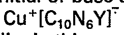
- Although the Cu2[C10N6]-2 molecular structure was shown in the above example, it is understood that other amphoteric molecular structures described earlier in Figures 8 and 9, or similar compounds, can form synthesized molecular complexes which exhibit optical multistate switching. It is also contemplated that such multistate synthetic molecules can be fabricated which have four or more switching states in accordance with the present invention.
- It must also be noted that Equation (6) represents a reversible electron transfer reaction and thermal energy generated by optical or thermal means can return all or part of the amphoteric material to the initial state. By this process, the memory medium formed from such synthetic amphoteric molecules can be "erased".
- The inventors have described three processes for forming a multistate amphoteric charge transfer medium. Generally, the amphoteric material is optically switched through a series of states by increasing the optical intensity. Figure 10 graphically illustrates the generalized optical switching characteristics. In the first or base state the organic switching medium is composed of redox species identified as "B" in Figure 10. An optical "write" beam is used to switch a spot on the material into a switched state (such spot referred as a "data storage spot"). If the optical intensity of the "write" beam exceeds an intensity threshold Ti, but is less than threshold T2, the illuminated spot will jump to the second state. The second state can be identified by the appearance of a new redox specie identified by A1 in Figure 10. (NOTE: The B redox species are still present at some reduced percentage and the Az and A3 redox states are essentially absent.) As noted earlier, optical and spectroscopic means, such Raman spectroscopy can identify the presence of the A1 redox species. If, however, the optical intensity exceeds T2 but is less than T3, the material in the illuminated spot will jump into the third state. In the third state, the B, A1, and A2 species are present and can be identified by optical or spectroscopic means. Similarly, if the optical threshold exceeds T3, the material in the illuminated spot will be switched to the fourth state, where the B, A,, A2 and A3 redox species are present. By identifying the redox species present at a particular "data storage spot", one can readily determine the switching state of that spot.
- Figure 11 is a truth table for such a generalized amphoteric system. The table shows that by identifying the presence of certain redox species, the state of the "data storage spot" can be determined. For example, if the A4 redox species is detected by optical means, it indicates that the "data storage spot" is in state 4. If, the A3 species is detected but not significant amounts of the A4 redox species, we are in the third state. If the A2 species is detected but not significant amounts of the A3 and A4 redox species, we are in the second state. If, however, the A2, A3 and A4 species are not significantly detected the "data storage spot" is in the first or base state.
- The switching phenomenon observed in such amphoteric charge transfer material can be either threshold switching or memory switching. For threshold switching the illuminated spot rapidly returns to the base state after the optical beam is removed. For memory switching, the illuminated spot requires additional energy to return to the lower thermodynamically stable state after the beam is removed. In most cases, ambient thermal energy is insufficient to rapidly reverse the electrochemical reaction back to the lower state (e.g., thermodynamically more stable state). The length of time memory can be retained depends on: (1) the particular material, (2) the diameter of the "write" beam; (3) the duration and intensity of the "write" beam; and (4) the thickness of amphoteric charge transfer film. In several cases it has been demonstrated that the greater the bonding energy between the donor and acceptor species the larger the threshold level needed to switch from one state to another and the greater likelihood that the switching action will be that of memory switching. Similarly, incident optical energy necessary to switch the amphoteric charge transfer material from one state to another depends on several factors including: (1) bonding energy; (2) size of the illumination "write" beam; (3) the duration of the optical "write" beam, and (4) the thickness or geometric arrangement of the amphoteric film or material. It will be noted that the frequency of the optical beam can be chosen from the ultraviolet, visible, and/or infrared regions of the electromagnetic spectrum.
- Application of heat energy to a portion of the amphoteric material, which may be generated by an optical source, causes the amphoteric material to return to a more thermodynamically stable state. If sufficient thermal energy is applied the amphoteric material will return to the base state. In the preferred apparatus, described later, the inventors used heat generated by a C02 laser to return a portion of the material to the base state.
- The multistate amphoteric charge transfer material described in this application, can be used as the optical storage medium in various optical switching and storage apparatus. Figure 12 is a schematic diagram of an optical storage system using such a multistate amphoteric charge transfer material as the optical storage medium. The amphoteric
charge transfer material 29 is deposited on or in a supportingbase material 31. The amphoteric material can be grown on a metaldonor base material 31, as described earlier in the specification, or other methods such as sputtering can deposit theamphoteric material 29 on thebase material 31. An optional transparentprotective coating 33 may be deposited on the surface of theamphoteric material film 29. An optical "write"beam 35 is focused on aspecific spot 37 on the surface of theamphoteric material 29. (This spot is referred to as a "data storage spot".) The optical "write" beam can be a high intensity light source or laser source such as an Argon or C02 laser focused to generate a field on the film surface in the area of the "data storage spot". The optical "write" beam has several discrete intensity levels, each intensity level causing the "data storage spot" to switch into a particular state. - Therefore, the intensity of the beam will cause the "data storage spot" to switch states - for example, in a three-state optical medium where the optical beam intensity is at the first threshold (T,) the "data storage spot" will switch from the base state to the second state; at intensity T2 the "data storage spot" will be switched to the third state; and, at an intensity of T3 the "data storage spot" will be switched into the fourth state. As mentioned previously, the optical intensity necessary to produce the above state changes depends on the choice of the amphoteric material, the film thickness or geometry and the area and intensity of the optical "write" beam.
- For memory systems, an optical "write" 35 can be directed by known optical or electrical control means to other "data" storage spot" locations on the surface of the amphoteric
charge transfer material 29 and can switch such other locations from the base state to one of several switch states. By controlling the beam intensity at a specific "data storage spot" location, multiple bits of data can be stored at that location in the optical storage medium. - For example, with an amphoteric organic charge transfer material, having a three-stage electron transfer reaction, an optical "write" beam can be used to switch the optical storage medium through the base state to one of three states depending on the intensity of the optical field strength. Therefore, the "write" beam could be used to store a three-bit data code at each "data storage spot". If the memory apparatus were used in conjunction with a binary computer, the first or base state could be represented by "01", the second switched state could be represented by a "10"; and, the third switched state could be represented by a "11 ". Alternatively, the memory apparatus could be used in connection with a base three computing system.
- Once data has been stored on the storage medium, a spectroscopic means can be used to determine the particular switched state of the "data storage spot" being evaluated. Figure 13 is a schematic of the spectroscopic means and shows "data storage spot"
localizations locations 37 with an intensity well below the first intensity threshold, so that the state atlocation 28 is not disturbed. The light source 41, for Raman spectroscopic analysis, could be a monochromatic source and Applicants suggest the use of a laser source. Reflected and/or emitted light 43 from the selected location on thefilm surface 37 is collected and filtered by the opticalband pass filter 45 allowing reflected light to pass through an optical means 47 for measuring the spectral intensity of each desired band. The optical means looks at the magnitude of particular spectral bands (Raman bands) which identify a particular redox species. (It would be possible to have a plurality of filter/detector combinations to measure the magnitude of reflected light in each band of interest. Alternatively, traditional Raman spectroscopic means could be utilized.) Based on the magnitude of the spectral intensity in each selected band,logic detection circuitry 48, of known design, determines the set of redox species present, which in turn uniquely defines the switched state of that "data storage spot". - The "reading" optical beam 41 can be directed by well known optical means to each of the plurality of "data storage spot" locations (e.g., 37, 38) on the surface of the amphoteric organic
charge transfer material 29 to determine the state of each particular location. That is to say, for an amphoteric charge transfer material having three states, the spectroscopic means will determine the state of a particular "data storage spot" and thereby determine the three-bit word stored at that "data storage spot". - Figure 14 is a schematic drawing showing the thermal erase means which is used to reverse the electrochemical charge transfer reaction and cause at least one of a plurality of "data storage spot" locations on the surface of the amphoteric organic
charge transfer material 29 to return to the base state. Figure 14 shows two alternative embodiments for the thermal erase means. The first embodiment uses thermal radiation from anoptical beam 49 focused on thelocation 37 to generate sufficient heat to switch the area back to the base state. Applicants have found that the C02 laser, with an intensity below the first threshold, can be focused onlocation 37 for a time period long enough to generate sufficient thermal energy to switch the location back to the base state, or more thermodynamically stable state. The optical heating beam 40 can be directed by a well known optical means to erase other locations on the amphoteric organic chargetransfer material surface 29. An alternative embodiment uses an electrical heating element 51, located belowsubstrate 31, to generate sufficient thermal energy to "erase" a portion of the amphoteric chargetransfer material film 29. - In an alternative embodiment, the
optical write beam 35, optical read beam 41, and theoptical heating beam 49, can be generated by a single laser source by varying the intensity and duration of the illuminating beam. It is within the contemplation of the Applicants that other well known means can be used to generate the desired optical "write/read" and "erase" beams, and to direct such beams to the desired location on the amphoteric organic charge transfer material surface. - Obviously many modifications and variations of the present invention are possible in light of the above teachings. It is therefore to be understood that within the scope of the appended claims the invention may be practiced otherwise than as specifically described.
Claims (29)


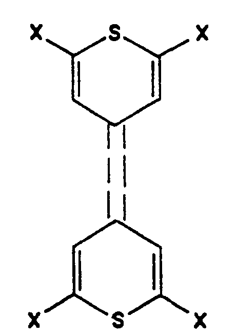
Applications Claiming Priority (2)
| Application Number | Priority Date | Filing Date | Title |
|---|---|---|---|
| US603717 | 1984-04-25 | ||
| US06/603,717 US4663270A (en) | 1984-04-25 | 1984-04-25 | Multistate optical switching and memory using an amphoteric organic charge transfer material |
Publications (3)
| Publication Number | Publication Date |
|---|---|
| EP0159397A2 EP0159397A2 (en) | 1985-10-30 |
| EP0159397A3 EP0159397A3 (en) | 1987-12-16 |
| EP0159397B1 true EP0159397B1 (en) | 1991-01-16 |
Family
ID=24416631
Family Applications (1)
| Application Number | Title | Priority Date | Filing Date |
|---|---|---|---|
| EP84113030A Expired EP0159397B1 (en) | 1984-04-25 | 1984-10-30 | Multistate optical switching and memory device using an organic charge transfer material |
Country Status (5)
| Country | Link |
|---|---|
| US (1) | US4663270A (en) |
| EP (1) | EP0159397B1 (en) |
| JP (1) | JPH07101512B2 (en) |
| CA (1) | CA1216942A (en) |
| DE (1) | DE3483966D1 (en) |
Families Citing this family (39)
| Publication number | Priority date | Publication date | Assignee | Title |
|---|---|---|---|---|
| US4825408A (en) * | 1984-04-25 | 1989-04-25 | The Johns Hopkins University | Multistate optical switching and memory apparatus using an amphoteric organic charge transfer material |
| US4684598A (en) * | 1984-11-23 | 1987-08-04 | The Johns Hopkins University | Enhanced optically sensitive medium using organic charge transfer materials to provide reproducible thermal/optical erasure |
| DE3507379A1 (en) * | 1985-03-02 | 1986-11-06 | Basf Ag, 6700 Ludwigshafen | OPTICAL RECORDING MEDIUM |
| US4871236A (en) * | 1985-09-18 | 1989-10-03 | Kabushiki Kaisha Toshiba | Organic thin film display element |
| EP0238759B1 (en) * | 1986-03-25 | 1992-03-11 | Kabushiki Kaisha Toshiba | Optical information writing method |
| JP2555048B2 (en) * | 1987-02-04 | 1996-11-20 | 株式会社日立製作所 | Optical recording method |
| WO1990001480A1 (en) * | 1988-07-29 | 1990-02-22 | Riedel-De Haen Aktiengesellschaft | Optical memory |
| US5161149A (en) * | 1991-07-22 | 1992-11-03 | The Johns Hopkins University | Electron density storage device and method using STM |
| DE69332710T2 (en) * | 1992-07-17 | 2004-01-15 | Biotechnology Res & Dev | SYSTEM FOR DETERMINING ATOMIC OR MOLECULAR SPECTRES AND / OR THESE THRESHOLD APPLICATIONS |
| NO301144B1 (en) * | 1995-05-23 | 1997-09-15 | Opticom As | Optical data storage |
| CA2377671C (en) * | 1999-07-01 | 2011-01-04 | David F. Bocian | High density non-volatile memory device |
| US6381169B1 (en) | 1999-07-01 | 2002-04-30 | The Regents Of The University Of California | High density non-volatile memory device |
| US6324091B1 (en) | 2000-01-14 | 2001-11-27 | The Regents Of The University Of California | Tightly coupled porphyrin macrocycles for molecular memory storage |
| WO2002077633A1 (en) | 2001-03-23 | 2002-10-03 | The Regents Of The University Of California | Open circuit potential amperometry and voltammetry |
| US6795778B2 (en) * | 2001-05-24 | 2004-09-21 | Lincoln Global, Inc. | System and method for facilitating welding system diagnostics |
| CN100419906C (en) * | 2001-08-13 | 2008-09-17 | 先进微装置公司 | memory unit |
| US6728129B2 (en) * | 2002-02-19 | 2004-04-27 | The Regents Of The University Of California | Multistate triple-decker dyads in three distinct architectures for information storage applications |
| US6746971B1 (en) | 2002-12-05 | 2004-06-08 | Advanced Micro Devices, Inc. | Method of forming copper sulfide for memory cell |
| US6770905B1 (en) | 2002-12-05 | 2004-08-03 | Advanced Micro Devices, Inc. | Implantation for the formation of CuX layer in an organic memory device |
| US6773954B1 (en) | 2002-12-05 | 2004-08-10 | Advanced Micro Devices, Inc. | Methods of forming passive layers in organic memory cells |
| WO2004070789A2 (en) * | 2003-02-03 | 2004-08-19 | The Regent Of The University Of California | Rewritable nano-surface organic electrical bistable devices |
| US6656763B1 (en) | 2003-03-10 | 2003-12-02 | Advanced Micro Devices, Inc. | Spin on polymers for organic memory devices |
| US6825060B1 (en) * | 2003-04-02 | 2004-11-30 | Advanced Micro Devices, Inc. | Photosensitive polymeric memory elements |
| US6977389B2 (en) * | 2003-06-02 | 2005-12-20 | Advanced Micro Devices, Inc. | Planar polymer memory device |
| US6787458B1 (en) | 2003-07-07 | 2004-09-07 | Advanced Micro Devices, Inc. | Polymer memory device formed in via opening |
| US6803267B1 (en) | 2003-07-07 | 2004-10-12 | Advanced Micro Devices, Inc. | Silicon containing material for patterning polymeric memory element |
| US7259039B2 (en) * | 2003-07-09 | 2007-08-21 | Spansion Llc | Memory device and methods of using and making the device |
| US7274035B2 (en) * | 2003-09-03 | 2007-09-25 | The Regents Of The University Of California | Memory devices based on electric field programmable films |
| US6955939B1 (en) | 2003-11-03 | 2005-10-18 | Advanced Micro Devices, Inc. | Memory element formation with photosensitive polymer dielectric |
| WO2005086627A2 (en) * | 2003-12-03 | 2005-09-22 | The Regents Of The University Of California | Three-terminal electrical bistable devices |
| US7608855B2 (en) * | 2004-04-02 | 2009-10-27 | Spansion Llc | Polymer dielectrics for memory element array interconnect |
| US7750341B2 (en) * | 2004-05-17 | 2010-07-06 | The Regents Of The University Of California | Bistable nanoparticle-polymer composite for use in memory devices |
| US7554111B2 (en) * | 2004-05-20 | 2009-06-30 | The Regents Of The University Of California | Nanoparticle-polymer bistable devices |
| US8044387B1 (en) | 2004-07-07 | 2011-10-25 | Spansion Llc | Semiconductor device built on plastic substrate |
| US20080089113A1 (en) * | 2004-10-28 | 2008-04-17 | The Regents Of The University Of California | Organic-Complex Thin Film For Nonvolatile Memory Applications |
| US7344913B1 (en) | 2005-04-06 | 2008-03-18 | Spansion Llc | Spin on memory cell active layer doped with metal ions |
| US20060238696A1 (en) * | 2005-04-20 | 2006-10-26 | Chien-Hui Wen | Method of aligning negative dielectric anisotropic liquid crystals |
| US20070009821A1 (en) * | 2005-07-08 | 2007-01-11 | Charlotte Cutler | Devices containing multi-bit data |
| US11311958B1 (en) * | 2019-05-13 | 2022-04-26 | Airgas, Inc. | Digital welding and cutting efficiency analysis, process evaluation and response feedback system for process optimization |
Family Cites Families (7)
| Publication number | Priority date | Publication date | Assignee | Title |
|---|---|---|---|---|
| GB1310812A (en) * | 1969-05-28 | 1973-03-21 | Ici Ltd | Radiation sensitive materials containing nitrogeneous cationic compounds |
| DE2314193A1 (en) * | 1972-06-01 | 1973-12-20 | Ibm | STORAGE ARRANGEMENT WITH A FILM OF ORGANIC MATERIAL |
| US4507672A (en) * | 1980-03-14 | 1985-03-26 | The Johns Hopkins University | Method of fabricating a current controlled bistable electrical organic thin film switching device |
| US4371883A (en) * | 1980-03-14 | 1983-02-01 | The Johns Hopkins University | Current controlled bistable electrical organic thin film switching device |
| US4394428A (en) * | 1981-09-24 | 1983-07-19 | Eastman Kodak Company | Photoconductive composition and elements comprising two different compounds having a dioxaborin nucleas on a derivative thereof |
| US4535042A (en) * | 1983-02-24 | 1985-08-13 | Hiroyuki Kitayama | Electrophotographic photosensitive member with electron donor and acceptor layers |
| JPH108421A (en) * | 1996-06-20 | 1998-01-13 | Tokai Rubber Ind Ltd | Bearing structure and construction method |
-
1984
- 1984-04-25 US US06/603,717 patent/US4663270A/en not_active Expired - Lifetime
- 1984-06-12 CA CA000456411A patent/CA1216942A/en not_active Expired
- 1984-10-30 EP EP84113030A patent/EP0159397B1/en not_active Expired
- 1984-10-30 DE DE8484113030T patent/DE3483966D1/en not_active Expired - Lifetime
- 1984-10-31 JP JP59230067A patent/JPH07101512B2/en not_active Expired - Lifetime
Also Published As
| Publication number | Publication date |
|---|---|
| JPH07101512B2 (en) | 1995-11-01 |
| CA1216942A (en) | 1987-01-20 |
| EP0159397A3 (en) | 1987-12-16 |
| US4663270A (en) | 1987-05-05 |
| DE3483966D1 (en) | 1991-02-21 |
| JPS60229249A (en) | 1985-11-14 |
| EP0159397A2 (en) | 1985-10-30 |
Similar Documents
| Publication | Publication Date | Title |
|---|---|---|
| US4663270A (en) | Multistate optical switching and memory using an amphoteric organic charge transfer material | |
| US4574366A (en) | Optical storage and switching devices using organic charge transfer salts | |
| Myles et al. | 1, 2‐Dithienylethene photochromes and non‐destructive erasable memory | |
| US5327373A (en) | Optoelectronic memories with photoconductive thin films | |
| EP0363147B1 (en) | Recording and reproducing apparatus and recording and reproducing method and recording medium for the recording and reproducing method | |
| EP0519745A2 (en) | Recording medium, information processing apparatus using same, and information-erasing method | |
| US4825408A (en) | Multistate optical switching and memory apparatus using an amphoteric organic charge transfer material | |
| US4507672A (en) | Method of fabricating a current controlled bistable electrical organic thin film switching device | |
| AU669136B2 (en) | Improved surface-enhanced raman optical data storage system | |
| EP0183168B1 (en) | An enhanced optically sensitive medium using organic charge transfer materials to provide reproducible thermal/optical erasure | |
| US4731756A (en) | Optical storage and switching devices using organic charge transfer salts | |
| JP4153756B2 (en) | Photochromic material | |
| US20040057372A1 (en) | Channeled dielectric re-recordable data storage medium | |
| Potember et al. | Electronic devices from conducting organics and polymers | |
| US4806995A (en) | Optical and electrical switching devices and a polymer composition containing pendant organic charge transfer salt moieties useful in switching devices | |
| US4735879A (en) | Recording media and recording methods | |
| CA1216358A (en) | Optical storage and switching devices using organic charge transfer salts | |
| US5026774A (en) | Polymer composition containing pendant organic charge transfer salt moieties useful in switching devices | |
| JP2004103044A (en) | Optical recording medium, method of manufacturing the same, and optical recording method | |
| JP3830771B2 (en) | Optical recording medium, processing apparatus and processing method thereof | |
| JPH02196689A (en) | Optical recording medium | |
| Huijser | Optical recording | |
| JPS60187953A (en) | Recording, reading and erasing method of information | |
| JPH0273548A (en) | Recording medium and recording and reproducing method | |
| JPS6070595A (en) | Photochemical hole burning optical memory |
Legal Events
| Date | Code | Title | Description |
|---|---|---|---|
| PUAI | Public reference made under article 153(3) epc to a published international application that has entered the european phase |
Free format text: ORIGINAL CODE: 0009012 |
|
| AK | Designated contracting states |
Designated state(s): DE FR GB SE |
|
| PUAL | Search report despatched |
Free format text: ORIGINAL CODE: 0009013 |
|
| AK | Designated contracting states |
Kind code of ref document: A3 Designated state(s): DE FR GB SE |
|
| 17P | Request for examination filed |
Effective date: 19880513 |
|
| 17Q | First examination report despatched |
Effective date: 19890419 |
|
| GRAA | (expected) grant |
Free format text: ORIGINAL CODE: 0009210 |
|
| AK | Designated contracting states |
Kind code of ref document: B1 Designated state(s): DE FR GB SE |
|
| PG25 | Lapsed in a contracting state [announced via postgrant information from national office to epo] |
Ref country code: SE Effective date: 19910116 Ref country code: FR Effective date: 19910116 |
|
| REF | Corresponds to: |
Ref document number: 3483966 Country of ref document: DE Date of ref document: 19910221 |
|
| EN | Fr: translation not filed | ||
| PLBE | No opposition filed within time limit |
Free format text: ORIGINAL CODE: 0009261 |
|
| STAA | Information on the status of an ep patent application or granted ep patent |
Free format text: STATUS: NO OPPOSITION FILED WITHIN TIME LIMIT |
|
| 26N | No opposition filed | ||
| PGFP | Annual fee paid to national office [announced via postgrant information from national office to epo] |
Ref country code: DE Payment date: 20001003 Year of fee payment: 17 |
|
| PGFP | Annual fee paid to national office [announced via postgrant information from national office to epo] |
Ref country code: GB Payment date: 20001004 Year of fee payment: 17 |
|
| PG25 | Lapsed in a contracting state [announced via postgrant information from national office to epo] |
Ref country code: GB Free format text: LAPSE BECAUSE OF NON-PAYMENT OF DUE FEES Effective date: 20011030 |
|
| REG | Reference to a national code |
Ref country code: GB Ref legal event code: IF02 |
|
| GBPC | Gb: european patent ceased through non-payment of renewal fee |
Effective date: 20011030 |
|
| PG25 | Lapsed in a contracting state [announced via postgrant information from national office to epo] |
Ref country code: DE Free format text: LAPSE BECAUSE OF NON-PAYMENT OF DUE FEES Effective date: 20020702 |