EP0150336A2 - Broadband radio frequency directional bridge - Google Patents
Broadband radio frequency directional bridge Download PDFInfo
- Publication number
- EP0150336A2 EP0150336A2 EP84114631A EP84114631A EP0150336A2 EP 0150336 A2 EP0150336 A2 EP 0150336A2 EP 84114631 A EP84114631 A EP 84114631A EP 84114631 A EP84114631 A EP 84114631A EP 0150336 A2 EP0150336 A2 EP 0150336A2
- Authority
- EP
- European Patent Office
- Prior art keywords
- port
- load
- taper
- conductor
- frequency
- Prior art date
- Legal status (The legal status is an assumption and is not a legal conclusion. Google has not performed a legal analysis and makes no representation as to the accuracy of the status listed.)
- Granted
Links
Images


Classifications
-
- G—PHYSICS
- G01—MEASURING; TESTING
- G01R—MEASURING ELECTRIC VARIABLES; MEASURING MAGNETIC VARIABLES
- G01R27/00—Arrangements for measuring resistance, reactance, impedance, or electric characteristics derived therefrom
- G01R27/02—Measuring real or complex resistance, reactance, impedance, or other two-pole characteristics derived therefrom, e.g. time constant
- G01R27/04—Measuring real or complex resistance, reactance, impedance, or other two-pole characteristics derived therefrom, e.g. time constant in circuits having distributed constants, e.g. having very long conductors or involving high frequencies
- G01R27/06—Measuring reflection coefficients; Measuring standing-wave ratio
-
- H—ELECTRICITY
- H01—ELECTRIC ELEMENTS
- H01P—WAVEGUIDES; RESONATORS, LINES, OR OTHER DEVICES OF THE WAVEGUIDE TYPE
- H01P1/00—Auxiliary devices
- H01P1/24—Terminating devices
- H01P1/26—Dissipative terminations
- H01P1/266—Coaxial terminations
-
- H—ELECTRICITY
- H01—ELECTRIC ELEMENTS
- H01P—WAVEGUIDES; RESONATORS, LINES, OR OTHER DEVICES OF THE WAVEGUIDE TYPE
- H01P5/00—Coupling devices of the waveguide type
- H01P5/08—Coupling devices of the waveguide type for linking dissimilar lines or devices
- H01P5/10—Coupling devices of the waveguide type for linking dissimilar lines or devices for coupling balanced lines or devices with unbalanced lines or devices
-
- H—ELECTRICITY
- H01—ELECTRIC ELEMENTS
- H01P—WAVEGUIDES; RESONATORS, LINES, OR OTHER DEVICES OF THE WAVEGUIDE TYPE
- H01P5/00—Coupling devices of the waveguide type
- H01P5/12—Coupling devices having more than two ports
- H01P5/16—Conjugate devices, i.e. devices having at least one port decoupled from one other port
- H01P5/19—Conjugate devices, i.e. devices having at least one port decoupled from one other port of the junction type
- H01P5/20—Magic-T junctions
Definitions
- This invention relates to a broadband radio frequency (R.F.) directional bridge and a broadband R.F. reference load that may be combined therewith in accordance with the preambles to claim 1 and, respectively, claim 14.
- R.F. radio frequency
- Such broadband R.F. directional bridges and R.F. loads are used for performing vector (phase and amplitude) measurements and time domain reflectometry in radio frequency circuits.
- a class of instruments called vector network analyzers is commonly employed for characterizing circuits in the frequency domain by providing plots of gain or loss, phase shift and reflection coefficients versus frequency.
- a directional bridge for separating reflected and transmitted signals from incident signals, e.g., in order to characterize the S-parameters of a device under test (D.U.T.).
- D.U.T. device under test
- Such a prior art bridge is shown in Figure 1.
- R3 termination resistor
- the circuit of Figure 1 is highly idealized. If the balun and termination are replaced by equivalent realistic impedances, the difficulties in constructing such a device become readily apparent.
- a corresponding equivalent circuit is shown in Figure 2.
- the parasitic shunt impedances ZB and ZC must be very large, i.e., ZB » RO and ZC » Z D.U.T. where Z D.U.T.
- the Wheatstone bridge is made up of a microcircuit which has a test port return loss of less than or equal to 20 dB over the entire range for frequencies from 45 MHz to 26.5 GHz. With a nominal impedance between the various ports (i.e., test port, reflection port, and reference port) of 50 ohms, this low return loss is accomplished by keeping the electrical path length in the various arms between ports at or below 0.1 the wavelength at the highest frequency.
- the precision termination has an essentially constant impedance over a very wide range of frequencies, the return loss being 40 dB or less from 1 GHz to 26.5 GHz and less than 34 dB from 45 MHz to 16 Hz.
- the termination has three distinct portions.
- a first portion having a continuous load element having inner taper of a relatively loss free dielectric and an outer taper of a lossy material, the combination providing a constant impedance in the higher frequencies. (This first continuous taper portion which is dielectrically loaded is useful by itself for a high frequency termination.)
- This first portion includes two additional tapered sections which are stepwise tapered to broaden the bandwidth of this first portion.
- a second portion of the precision termination is made up of a lumped load attached to the tapered portion.
- a third portion includes a ferrite bead distributed load attached to the lumped load opposite the tapered load.
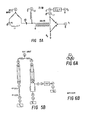
- FIG. 3 Shown in Figure 3 is a design for an R.F. terminated Wheatstone bridge which does not require either high shunt impedance or delicate balancing.
- the shunt impedance ZC is substantially eliminated and ZB is made to be R0, where RO is a constant impedance (typically 50 ohms) over the frequencies of interest, thus eliminating the separate resistor for that function and achieving a balanced bridge.
- RO is a constant impedance (typically 50 ohms) over the frequencies of interest, thus eliminating the separate resistor for that function and achieving a balanced bridge.
- the first, R01 is a high frequency distributed load for preventing signals at the reference port from seeing any shunt impedance other than R0. Unlike an isolated lumped resistor which provides virtually no isolation, such a distributed load can be made to provide almost any degree of isolation commensurate with acceptable dimensions. Such isolation requires, however, that there be sufficient loss per unit length to avoid introducing shunt impedance at the frequencies of interest. Losses of 20-25 dB along the length of the load (40-50 dB isolation) are generally sufficient to avoid bridge imbalance.
- the second stage of the reference impedance, R02 is a lumped load placed at the end of R01 to provide a termination at lower frequencies where losses in the distributed load, R01, are insufficient to achieve isolation.
- the third stage, R03 a ferrite core (balun), is added to keep the shunt reactance high.
- the magnitude of the impedances of R02 and R03 are chosen so that their combined parallel impedance is equal to RO since R01 is transparent at low frequencies.
- test port T can be D.C. biased by means of center conductor C1 (e.g., to provide power to transistors and I.C.'s in the D.U.T.).
- center conductor C1 e.g., to provide power to transistors and I.C.'s in the D.U.T.
- FIG. 5A Such a reflectometer design is illustrated schematically in Figure 5A.
- the balun and R' represent the reference impedance R0.
- the system is fed through an R.F. power splitter 11 to provide a reference signal and to supply power to the bridge.
- bl corresponds to the signal at port R and b2 corresponds to the signal after transmission through the D.U.T.
- the vector ratio bl/al is proportional to the input reflection coefficient while b2/al is proportional to the transmission coefficient of the D.U.T..
- a D.C. block 12 for isolating the R.F. power input from the bias voltage provided by bias input 13 on the center conductor of the reference impedance R0. Shown in Figure 5B is a typical reflection/transmission test setup which is particularly adopted for use by an automated R.F. network analyzer.
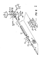
- a practical implementation of the bridge and the accompanying precision broadband load assembly is depicted in a somewhat exploded view in Figure 6.
- the system is made up of a bridge assembly housing 1, which contains a bridge microcircuit 6 (shown in enlarged view in Figure 6A) for providing electrical connections between the reflection port, the test port and the reference port.
- a bridge microcircuit 6 shown in enlarged view in Figure 6A
- housing 1 also included in housing 1 is an adjustable spring loaded top ground plane 2.
- a coax assembly 3 for connecting the high frequency portion R01 of the reference load to the reference port of the microwave bridge. This is accomplished by providing a tapered transition from center coax 10 of R01 to center coax 7 of the reference port which feeds microcircuit 6 the transition being accomplished by means of an inner taper 9 and an outer taper 8.
- the lumped load R02 which is made up of a 61.5 ohm resistor 22 and an inner conductor 24 and outer conductor 23.
- Attached to lumped load R02 is the balun section R03 made up of a series of ferrite beads, such as bead 21, located on the coax.
- the impedance of R03 is generally chosen to be about 285 ohms in order to provide a combined shunt impedance with R02 of 50 ohms.
- Balun R03 is typically formed into a single loop for mechanical stress relief purposes and a pad of polyurethane foam 26 is formed around it for protection from impact.
- Coax assembly 16 then provides connection for R.F. input and D.C. bias, and a grommet 5 is used to stabilize the positions of loads R02 and R03 in a load shroud assembly 17.
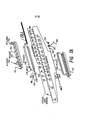
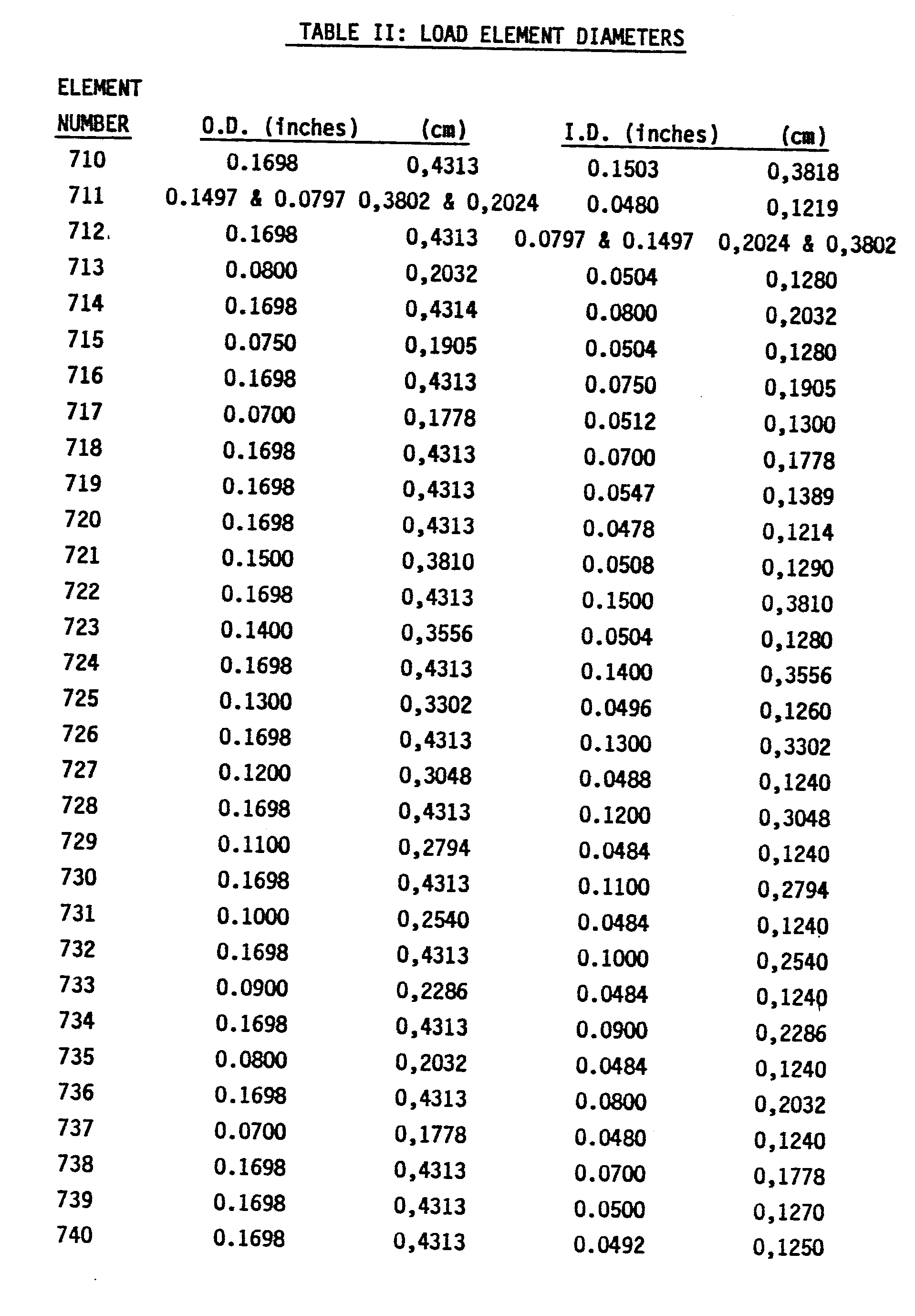
- FIG. 7A Shown in Figure 7A is an expanded view of distributed load R01 and lumped load R02. For purposes of discussion, all elements not already described previously will be numbered in the 700's to associate that element with Figure 7.
- Element 701 is a bottom ground plane, typically aluminum, having a groove therein to accommodate the distributed load material of the triaxial structure.
- Tapered loads 711 and 712 typically provide a constant impedance distributed load for frequencles above about 8 GHz, while the balance of the loads 711 and 713 through 740 are for achieving a flat response in the intermediate frequency ranges. As illustrated in Figure 7B, tapered loads 711 and 712 are physically mated to achieve a snug fit.
- Tapered load 711 is typically constructed of a relatively lossless material such as cross-linked polystyrene having a relative dielectric constant of about 2.54 (e.g., STYCAST 0005, which is manufactured by Emerson & Cuming) so that the distributed load is dielectrically loaded on the front end rather than relying on air as the dielectric. This dielectric loading is very important in achieving the desired matching characteristics with the lumped load.
- the preferred diameter is about 0.1497 inches (0,3802 cm), while at the distal end the preferred diameter is about 0.0797 inches (0,2024 cm).
- tapered load 711 The preferred length for tapered load 711 is generally about 1.959 inches (4,9759 cm) with taper beginning about 0.230 inches (0,5842 cm) from the front.
- Tapered load 712 is typically constructed of a machineable lossy material such as MF112 which is also manufactured by Emerson & Cuming. Table I provides a list of the electromagnetic characteristics of MF112 relative to the vacuum as a function of frequency.
- the balance of the distributed load i.e., loads 13 through 40, carries through this tapered load concept, except that the loads are stepwise tapered.
- step tapered terminations have a relatively narrow bandwidth and critical dimensionality.
- lossy loads in multiple steps (i.e., multiple loads) the bandwidth can be increased while at the same time reducing the overall length of the distributed load section.
- lossy loads provides a forgiving structure, since subsequent losses in successive loads tends to obscure reflections at interfaces between loads.
- inner loads 713, 715, 717, and load spacer 720 are typically constructed of STYCAST 0005 material, while outer loads 714, 716, 718, and 719, and inner loads 721, 723, 725, 727, 729, 731, 733, 735, and 737 are typically constructed of MF112 material.
- the second stepwise taper begins at load 722 and continues through load 740, with loads 722, 724, 726, 728, 730, 732, 734, 736, 738, 739, and 740 being constructed of MF124, a material produced by Emerson & Cuming which has a substantially higher loss than MF112.
- Table I also lists the electromagnetic characteristics of MF124 as a function of frequency. MF112 and MF124 were chosen because they are a mixture of lossy elements in a base material which is the same as STYCAST 0005. Hence, at low frequencies where the lossy elements have a minimal loss contribution, the outer taper resembles the inner taper, so that the distributed portion and the lumped load termination together are essentially matched to the reference im - pedance.
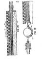
- Table II is a list of the inside and outside diameters of each of the loads. The linear dimension of each load is 0.25 inches (0,635 cm), except for load 719 which is 0.230 inches (0,5842 cm) long and load 719 which together with load spacer 720 totals 0.25 inches (0,635 cm). As indicated in drawings 7A, 78, and 7C, the loads are strung in close contact on a center conductor 705. The diameter of center conductor 705 is nominally 0.0474 inches (0,1204 cm).
- Holding loads 710 through 740 in place is an adjustable top ground plane 741, typically constructed of gold-plated berylliumcopper and nominally having a width W of 0.237 inches (0,6020 cm), a depth D of 0.197 inches (0,5004 cm), and a length L of 5.735 inches (14,567 cm) (see Figures 7A and 7E). Holes in the top of ground plane 741 permit press blocks 748 to extend through the top surface to contact conductive shoes 747 which in turn contact the lower flanges of the top ground plane, in order to push them into firm contact with the load elements (see Figure 7D for a cross-section showing the deformation of the top ground plane on the outer surface of the load).
- the force for press blocks 748 is furnished by set screws 755 and 756 mounted in a top housing 753. This ability to tune the individual load elements via the top ground plane is particularly important in achieving a precision load since steptapered loads can be particularly sensitive to small changes in magnetic and dielectric properties. It should also be noted that throughout the system, RFI round strip conductive elastomeric gaskets 708 are provided to insure good electrical contact.
- Shown in Figure 7C is the tail end of the reference load illustrating the single loop of the inner coax threaded through a sequence of nine (9) ferrite shielding beads 757.
- Such beads are used because they have a high magnetic permeability and are very lossy, so that when the inner coax is eventually shorted to ground, there will be enough series loss to isolate the short and provide a precision reference termination.
- a typical material for beads 757 is Ferroxcube material 3B (available from Hewlett-Packard Company as stock number 9170-0016), having an initial magnetic permeability of 900 relative to the vacuum at 20 degrees Celsius.
- Beads 757 typically have an inner diameter of 0.051 inches (0,1295 cm), and outer diameter of 0.138 inches (0,3505 cm), and are 0.159 inches (0,4039 cm) long, so as to achieve an impedance of 300 ohms in this balun section.
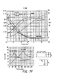
- Figure 7F is a plot of the electrical characteristics of beads 757.
- FIG. 7G Shown in Figure 7G is an expanded view of lumped resistor 709 (the equivalent of R02 of Figure 3). It is generally constructed by connecting inner and outer rings of gold-coated sapphire with eight identical, equally spaced, resistors 758 to obtain a combined resistance of 61.5 ohms.
- the outer diameter of the outer ring of the sapphire substrate is typically 0.345 inches (0,8763 cm) and the inner diameter is typically 0.270 inches (0,6858 cm).
- Resistors 758 are generally constructed of tantalum.
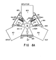
- FIG 8A Shown in Figure 8A is a magnified view of microcircuit 6 which was described briefly in reference to Figure 6.
- the microcircuit is formed on a hexagonal sapphire substrate 801 (shown in detail in Figure 8B) which has a nominal thickness of 10 mils (0,254 mm).
- the circuit has reflection symmetry in a plane passing through the center of reflection port 823 and the center of the circuit 804.
- the hexagon is not regular.
- Opposite sites are parallel, sides 802, 803, and 804 are equal in length, and sides 805 and 807 are equal in length.
- side 802 is not the same length as 805 or 806.
- Table III gives a list of preferred dimensions for the microcircuit.
- the gold pattern and tantalum resistors 809, 810, 811, and 812 shown in Figures 8A and 8B are put down on both faces of the substrate with resistors on one-face being disposed immediately opposite resistors on the other face.
- the resistance of each resistor 809, 810, 811, and 812 and their counterparts on the opposite face of the substrate is nominally 50.0 ohms-, so that the combined resistance in each leg, i.e., between the reflection port and the reference port is 50 ohms and between the reflection port and the test port is 50 ohms. This results from the fact that each leg has a series resistance of 100 ohms on each face, and the two faces provide parallel connections to the ports.
- Arrowheads 821, 822, and 823 for providing electrical and mechanical connections to each port are typically constructed of beryllium copper turned on a numerically controlled screw machine to a diameter of 0.060 inches (0,1524 cm).
- the overall length of the arrowheads is 0.080 inches (0,2032 cm) and includes a cone portion having a length of 0.037 inches (0,0940 cm) to avoid introducing unwanted capacitance into the system.
- Each cone portion is slotted to a width of about 11 mils (0,279 mm) to accommodate the 10 mil (0,254 mm) substrate and is soldered to the substrate via solder holes such as 824.
- Each arrowhead is gold plated to insure good electrical contact.
- inner coax 825 which extends through the reference port arrowhead. Its center conductor 826 bridges a gap 827 of about 0.003 inches (0,076 mm) and makes contact with a dummy coax 829 which electrically connects center conductor 826 directly to the test port. Gap 827 then acts as an R.F. generator midway between the test and reference ports.
- the diameter of conductor 829 typically 0.013 inches (0,330 mm), is the same as the diameter of inner coax 825 in order to maintain electrical and physical symmetry as to both the test port and reference port.
- the transmission lines from the generator to the test port and reflection port should be 25 ohms for best termination (since the reflection port looks like a virtual ground because of the symmetry of the device).
- the desired impedance should look like 100 ohms in each branch, i.e., from the test port to ground through the reflection port,and from the test port to ground through the reference port.
- the microcircuit itself is made very small in order that the parasitic impedances introduced by the microcircuit are small relative to the 50 ohm operating impedance.
- the corresponding maximum desired electrical path length between ports can be calculated using the following relationship: where B is the electrical path length.
- microcircuit 6 is mechanically supported totally by its electrical connections.
- outer coax 901 supports the microcircuit at the reference port.
- the end most tip of outer coax 901 is typically hemispherical in shape with a hole therethrough to accommodate inner coax 825, and contacts the drilled end 921 of arrowhead 821.
- the test port of the microcircuit is supported by a spring loaded ball joint 903 which contacts the drilled end 922 of arrowhead 822.
- the reflection port is supported by a spring loaded piece of slabline 905 which rests in a slot 923 cut in the end of arrowhead 823.
Landscapes
- Physics & Mathematics (AREA)
- General Physics & Mathematics (AREA)
- Measurement Of Resistance Or Impedance (AREA)
- Non-Reversible Transmitting Devices (AREA)
- Waveguides (AREA)
Abstract
Description
- This invention relates to a broadband radio frequency (R.F.) directional bridge and a broadband R.F. reference load that may be combined therewith in accordance with the preambles to claim 1 and, respectively, claim 14. Such broadband R.F. directional bridges and R.F. loads are used for performing vector (phase and amplitude) measurements and time domain reflectometry in radio frequency circuits.
- A class of instruments called vector network analyzers is commonly employed for characterizing circuits in the frequency domain by providing plots of gain or loss, phase shift and reflection coefficients versus frequency. At the heart of such measuring instruments is a directional bridge for separating reflected and transmitted signals from incident signals, e.g., in order to characterize the S-parameters of a device under test (D.U.T.). Such a prior art bridge is shown in Figure 1. Here the device is typically symmetric relative to the R.F. input, with the resistance of resistors Rl and R2 being equal to each other, and equal in value to that of load resistor R0, i.e., R1 = R2 = R0. The device is typically implemented with a balun B between reference port (R) and test port (T), and with a termination resistor R3 = RO for extracting the signal. As a practical matter, however, the circuit of Figure 1 is highly idealized. If the balun and termination are replaced by equivalent realistic impedances, the difficulties in constructing such a device become readily apparent. A corresponding equivalent circuit is shown in Figure 2. Here, R1 = R2 = RO as before. However, for satisfactory measurements the following requirements must be satisfied: (1) the parasitic shunt impedances ZB and ZC must be very large, i.e., ZB » RO and ZC » Z D.U.T. where Z D.U.T. is the impedance of the device under test; or (2) ZB and ZC must be extremely well balanced, i.e., ZB = ZC exactly; or (3) ZB and ZC must satisfy some relation which is a compromise between (1) and (2) above. For measuring instruments which are restricted to a few octaves or less in bandwidth, these restrictions can usually be met without extreme measures. However, above 1 to 2 GHz, it becomes very difficult to produce a broadband impedance greater than about 1 K ohm, since the impedance decreases rapidly with increasing frequency. Hence, higher frequencies impose very stringent requirements for balancing of the two shunt impedances. As a result, for very wide bandwidth devices, e.g., over the entire range from 45 MHz to 26.5 GHz, it does not appear physically possible with the present state of the art to provide such high impedances or such precise balancing. Nevertheless, wide bandwidth directional bridges are highly desirable for automated test equipment using broadband sweepers to characterize circuit parameters and are particularly important for performing Fourier transforms for accurate time domain reflectometry, a technique which has proven extremely useful in solving intricate design problems. To date, the practical difficulties of extracting the desired differential signal over such a wide bandwidth without introducing unbalanced parasitic impedances haveeluded the industry.
- Relative to this prior art the invention claimed in claims 1 and 6 solves the problem of providing a design for a terminated R.F./ microwave Wheatstone bridge and a precision termination which can be used therewith over a broader frequency range than has previously been possible.
- The Wheatstone bridge is made up of a microcircuit which has a test port return loss of less than or equal to 20 dB over the entire range for frequencies from 45 MHz to 26.5 GHz. With a nominal impedance between the various ports (i.e., test port, reflection port, and reference port) of 50 ohms, this low return loss is accomplished by keeping the electrical path length in the various arms between ports at or below 0.1 the wavelength at the highest frequency.
- The precision termination has an essentially constant impedance over a very wide range of frequencies, the return loss being 40 dB or less from 1 GHz to 26.5 GHz and less than 34 dB from 45 MHz to 16 Hz. The termination has three distinct portions. A first portion having a continuous load element having inner taper of a relatively loss free dielectric and an outer taper of a lossy material, the combination providing a constant impedance in the higher frequencies. (This first continuous taper portion which is dielectrically loaded is useful by itself for a high frequency termination.) This first portion, however, includes two additional tapered sections which are stepwise tapered to broaden the bandwidth of this first portion. A second portion of the precision termination is made up of a lumped load attached to the tapered portion. A third portion includes a ferrite bead distributed load attached to the lumped load opposite the tapered load.
- An embodiment of the invention will now be discussed in detail with reference to the accompanying drawings. In the drawings,
- Fig. 1 shows a typical prior art bridge;
- Fig. 2 shows an equivalent circuit for an actual bridge in accordance with Figure 1;
- Fig. 3 shows a terminated Wheatstone bridge in accordance with the invention;
- Fig. 4 shows a reference load according to the invention;
- Fig. 5A shows a reflectometer configuration using a bridge according to the invention;
- Fig. 5B shows a reflection/transmission setup for use in an automated network analyzer;
- Fig. 6, 6A and 6B show an exploded view of the bridge system and reference port;
- Fig. 7A, 7B, 7C, 7D, and 7E show expanded views of the reference load and its elements;
- Fig. 8A, 8B depict a microcircuit in the terminated Wheatstone bridge according to the invention; and
- Fig. 9 is a cross-sectional view of the bridge housing.
- Shown in Figure 3 is a design for an R.F. terminated Wheatstone bridge which does not require either high shunt impedance or delicate balancing. Here all the elements and relationships are the same as those in Figure 2, except that the shunt impedance ZC is substantially eliminated and ZB is made to be R0, where RO is a constant impedance (typically 50 ohms) over the frequencies of interest, thus eliminating the separate resistor for that function and achieving a balanced bridge. With this structure, it can be shown by simple circuit analysis that the floating voltage VT, generated across the terminating impedance ZA, is proportional to the reflection coefficient of the D.U.T.
- While the built-in detector of a scalar bridge can easily convert the floating R.F. voltage VT to a single-ended D.C. output, the vector bridge of Figure 3 is faced with a much more severe challenge. It must extract the floating R.F. signal and feed it to a single ended vector detection system, without upsetting the delicate symmetry and impedance level of the bridge. For this reason, it should be readily apparent that RO must be a precision element with a flat response over the entire frequency range of interest, which in the preferred embodiment is generally from 45 MHz to 26.5 GHz. In order to provide such a constant impedance over this large bandwidth, RO is typically a composite system as depicted in Figure 4. As illustrated, RO has three distinct elements. The first, R01, is a high frequency distributed load for preventing signals at the reference port from seeing any shunt impedance other than R0. Unlike an isolated lumped resistor which provides virtually no isolation, such a distributed load can be made to provide almost any degree of isolation commensurate with acceptable dimensions. Such isolation requires, however, that there be sufficient loss per unit length to avoid introducing shunt impedance at the frequencies of interest. Losses of 20-25 dB along the length of the load (40-50 dB isolation) are generally sufficient to avoid bridge imbalance.
- The second stage of the reference impedance, R02, is a lumped load placed at the end of R01 to provide a termination at lower frequencies where losses in the distributed load, R01, are insufficient to achieve isolation. To avoid parasitic shunt impedances at these lower frequencies, the third stage, R03, a ferrite core (balun), is added to keep the shunt reactance high. The magnitude of the impedances of R02 and R03 are chosen so that their combined parallel impedance is equal to RO since R01 is transparent at low frequencies.
- Another important feature of this structure is its triaxial nature, i.e., having a center conductor C1 inside a coaxial conducting sheath C2, which is itself inside a second coaxial conductor C3. Because the input and detector ports of a vector bridge are functionally interchangeable, either port may be driven while the other extracts the reflected signal. Hence, by reversing the orientation from that shown in Figure 4 and driving from the balun end R03, the test port T can be D.C. biased by means of center conductor C1 (e.g., to provide power to transistors and I.C.'s in the D.U.T.). Such a reflectometer design is illustrated schematically in Figure 5A. Here the balun and R' represent the reference impedance R0. The system is fed through an R.F. power splitter 11 to provide a reference signal and to supply power to the bridge. bl corresponds to the signal at port R and b2 corresponds to the signal after transmission through the D.U.T.
- The vector ratio bl/al is proportional to the input reflection coefficient while b2/al is proportional to the transmission coefficient of the D.U.T.. Also, included is a
D.C. block 12 for isolating the R.F. power input from the bias voltage provided bybias input 13 on the center conductor of the reference impedance R0. Shown in Figure 5B is a typical reflection/transmission test setup which is particularly adopted for use by an automated R.F. network analyzer. - A practical implementation of the bridge and the accompanying precision broadband load assembly is depicted in a somewhat exploded view in Figure 6. The system is made up of a bridge assembly housing 1, which contains a bridge microcircuit 6 (shown in enlarged view in Figure 6A) for providing electrical connections between the reflection port, the test port and the reference port. Also included in housing 1 is an adjustable spring loaded
top ground plane 2. Also shown is a coax assembly 3 for connecting the high frequency portion R01 of the reference load to the reference port of the microwave bridge. This is accomplished by providing a tapered transition from center coax 10 of R01 to center coax 7 of the reference port which feeds microcircuit 6 the transition being accomplished by means of an inner taper 9 and anouter taper 8. At the other end of the distributed portion of the R01 reference load is the lumped load R02 which is made up of a 61.5ohm resistor 22 and aninner conductor 24 andouter conductor 23. Attached to lumped load R02 is the balun section R03 made up of a series of ferrite beads, such as bead 21, located on the coax. The impedance of R03 is generally chosen to be about 285 ohms in order to provide a combined shunt impedance with R02 of 50 ohms. - Balun R03 is typically formed into a single loop for mechanical stress relief purposes and a pad of
polyurethane foam 26 is formed around it for protection from impact.Coax assembly 16 then provides connection for R.F. input and D.C. bias, and agrommet 5 is used to stabilize the positions of loads R02 and R03 in aload shroud assembly 17. - Shown in Figure 7A is an expanded view of distributed load R01 and lumped load R02. For purposes of discussion, all elements not already described previously will be numbered in the 700's to associate that element with Figure 7.
Element 701 is a bottom ground plane, typically aluminum, having a groove therein to accommodate the distributed load material of the triaxial structure.Tapered loads loads loads Tapered load 711 is typically constructed of a relatively lossless material such as cross-linked polystyrene having a relative dielectric constant of about 2.54 (e.g.,STYCAST 0005, which is manufactured by Emerson & Cuming) so that the distributed load is dielectrically loaded on the front end rather than relying on air as the dielectric. This dielectric loading is very important in achieving the desired matching characteristics with the lumped load. At the front end of taperedload 711 the preferred diameter is about 0.1497 inches (0,3802 cm), while at the distal end the preferred diameter is about 0.0797 inches (0,2024 cm). The preferred length for taperedload 711 is generally about 1.959 inches (4,9759 cm) with taper beginning about 0.230 inches (0,5842 cm) from the front.Tapered load 712 is typically constructed of a machineable lossy material such as MF112 which is also manufactured by Emerson & Cuming. Table I provides a list of the electromagnetic characteristics of MF112 relative to the vacuum as a function of frequency. - The balance of the distributed load, i.e., loads 13 through 40, carries through this tapered load concept, except that the loads are stepwise tapered. Generally step tapered terminations have a relatively narrow bandwidth and critical dimensionality. However, by using lossy loads in multiple steps (i.e., multiple loads) the bandwidth can be increased while at the same time reducing the overall length of the distributed load section. In addition, the use of lossy loads provides a forgiving structure, since subsequent losses in successive loads tends to obscure reflections at interfaces between loads. As indicated in Figure 7A in the first stepwise taper,
inner loads STYCAST 0005 material, whileouter loads 714, 716, 718, and 719, and inner loads 721, 723, 725, 727, 729, 731, 733, 735, and 737 are typically constructed of MF112 material. The second stepwise taper begins at load 722 and continues through load 740, with loads 722, 724, 726, 728, 730, 732, 734, 736, 738, 739, and 740 being constructed of MF124, a material produced by Emerson & Cuming which has a substantially higher loss than MF112. Table I also lists the electromagnetic characteristics of MF124 as a function of frequency. MF112 and MF124 were chosen because they are a mixture of lossy elements in a base material which is the same asSTYCAST 0005. Hence, at low frequencies where the lossy elements have a minimal loss contribution, the outer taper resembles the inner taper, so that the distributed portion and the lumped load termination together are essentially matched to the reference im- pedance. Table II is a list of the inside and outside diameters of each of the loads. The linear dimension of each load is 0.25 inches (0,635 cm), except for load 719 which is 0.230 inches (0,5842 cm) long and load 719 which together with load spacer 720 totals 0.25 inches (0,635 cm). As indicated in drawings 7A, 78, and 7C, the loads are strung in close contact on acenter conductor 705. The diameter ofcenter conductor 705 is nominally 0.0474 inches (0,1204 cm). - Holding loads 710 through 740 in place is an adjustable
top ground plane 741, typically constructed of gold-plated berylliumcopper and nominally having a width W of 0.237 inches (0,6020 cm), a depth D of 0.197 inches (0,5004 cm), and a length L of 5.735 inches (14,567 cm) (see Figures 7A and 7E). Holes in the top ofground plane 741 permit press blocks 748 to extend through the top surface to contactconductive shoes 747 which in turn contact the lower flanges of the top ground plane, in order to push them into firm contact with the load elements (see Figure 7D for a cross-section showing the deformation of the top ground plane on the outer surface of the load). The force for press blocks 748 is furnished byset screws top housing 753. This ability to tune the individual load elements via the top ground plane is particularly important in achieving a precision load since steptapered loads can be particularly sensitive to small changes in magnetic and dielectric properties. It should also be noted that throughout the system, RFI round strip conductiveelastomeric gaskets 708 are provided to insure good electrical contact. - Shown in Figure 7C is the tail end of the reference load illustrating the single loop of the inner coax threaded through a sequence of nine (9)
ferrite shielding beads 757. Such beads are used because they have a high magnetic permeability and are very lossy, so that when the inner coax is eventually shorted to ground, there will be enough series loss to isolate the short and provide a precision reference termination. A typical material forbeads 757 is Ferroxcube material 3B (available from Hewlett-Packard Company as stock number 9170-0016), having an initial magnetic permeability of 900 relative to the vacuum at 20 degrees Celsius.Beads 757 typically have an inner diameter of 0.051 inches (0,1295 cm), and outer diameter of 0.138 inches (0,3505 cm), and are 0.159 inches (0,4039 cm) long, so as to achieve an impedance of 300 ohms in this balun section. Figure 7F is a plot of the electrical characteristics ofbeads 757. - Shown in Figure 7G is an expanded view of lumped resistor 709 (the equivalent of R02 of Figure 3). It is generally constructed by connecting inner and outer rings of gold-coated sapphire with eight identical, equally spaced,
resistors 758 to obtain a combined resistance of 61.5 ohms. - The outer diameter of the outer ring of the sapphire substrate is typically 0.345 inches (0,8763 cm) and the inner diameter is typically 0.270 inches (0,6858 cm).
- The outer diameter of the inner ring is typically 0.135 inches (0,3429 cm) and the inner diameter of the inner ring is typically 0.075 inches (0,1905 cm).
Resistors 758 are generally constructed of tantalum. - Shown in Figure 8A is a magnified view of microcircuit 6 which was described briefly in reference to Figure 6. The microcircuit is formed on a hexagonal sapphire substrate 801 (shown in detail in Figure 8B) which has a nominal thickness of 10 mils (0,254 mm). Geometrically, the circuit has reflection symmetry in a plane passing through the center of
reflection port 823 and the center of thecircuit 804. However, the hexagon is not regular. Opposite sites are parallel, sides 802, 803, and 804 are equal in length, andsides side 802 is not the same length as 805 or 806. Table III gives a list of preferred dimensions for the microcircuit. Typically, the gold pattern andtantalum resistors resistor gold pads 819 andcapacitors 814. Each capacitor is nominally 350 picofarads, and capacitors on opposite faces of the substrate are oriented in opposite direction for symmetry reasons. -
Arrowheads center conductor 826 bridges agap 827 of about 0.003 inches (0,076 mm) and makes contact with a dummy coax 829 which electrically connectscenter conductor 826 directly to the test port.Gap 827 then acts as an R.F. generator midway between the test and reference ports. The diameter ofconductor 829, typically 0.013 inches (0,330 mm), is the same as the diameter of inner coax 825 in order to maintain electrical and physical symmetry as to both the test port and reference port. - Despite the efforts at maintaining electrical and physical symmetry between ports, it is important to note that such symmetry alone is not sufficient to achieve an adequate port match. This can be most easily seen by noting that looking into the microcircuit from the generator with the test port terminated in 50 ohms, the transmission lines from the generator to the test port and reflection port should be 25 ohms for best termination (since the reflection port looks like a virtual ground because of the symmetry of the device). However, on terminating the reflection port in 50 ohms instead of the test port and looking into the microcircuit from the test port, the desired impedance should look like 100 ohms in each branch, i.e., from the test port to ground through the reflection port,and from the test port to ground through the reference port. To accommodate this poor port match, the microcircuit itself is made very small in order that the parasitic impedances introduced by the microcircuit are small relative to the 50 ohm operating impedance. By deciding on a design criterion for test port return loss, the corresponding maximum desired electrical path length between ports can be calculated using the following relationship:

- Another unique feature of microcircuit 6 is that it is mechanically supported totally by its electrical connections. As illustrated in Figure 9, which is a cross-section of housing 1, outer coax 901, supports the microcircuit at the reference port. The end most tip of outer coax 901 is typically hemispherical in shape with a hole therethrough to accommodate inner coax 825, and contacts the drilled end 921 of
arrowhead 821. The test port of the microcircuit is supported by a spring loaded ball joint 903 which contacts the drilled end 922 ofarrowhead 822. The reflection port is supported by a spring loaded piece ofslabline 905 which rests in aslot 923 cut in the end ofarrowhead 823. This manner of three element mechanical support permits very stable mounting which also permits electrical adjustment within the housing by placing adjustingscrews bottom ground plane 910 of housing 1, as shown in fig. 6, directly under the joint between each arrowhead and its electrical/ mechanical connection.

Claims (18)
characterized in that said microcircuit comprises:
characterized by
Applications Claiming Priority (2)
| Application Number | Priority Date | Filing Date | Title |
|---|---|---|---|
| US568986 | 1984-01-09 | ||
| US06/568,986 US4588970A (en) | 1984-01-09 | 1984-01-09 | Three section termination for an R.F. triaxial directional bridge |
Related Child Applications (1)
| Application Number | Title | Priority Date | Filing Date |
|---|---|---|---|
| EP89103821.8 Division-Into | 1989-03-04 |
Publications (3)
| Publication Number | Publication Date |
|---|---|
| EP0150336A2 true EP0150336A2 (en) | 1985-08-07 |
| EP0150336A3 EP0150336A3 (en) | 1986-02-12 |
| EP0150336B1 EP0150336B1 (en) | 1991-08-28 |
Family
ID=24273607
Family Applications (1)
| Application Number | Title | Priority Date | Filing Date |
|---|---|---|---|
| EP84114631A Expired - Lifetime EP0150336B1 (en) | 1984-01-09 | 1984-12-01 | Broadband radio frequency directional bridge |
Country Status (4)
| Country | Link |
|---|---|
| US (1) | US4588970A (en) |
| EP (1) | EP0150336B1 (en) |
| JP (1) | JPH0795645B2 (en) |
| DE (2) | DE3486157T2 (en) |
Cited By (3)
| Publication number | Priority date | Publication date | Assignee | Title |
|---|---|---|---|---|
| EP0554021A3 (en) * | 1992-01-27 | 1994-08-10 | Marconi Instruments Ltd | Circuits for use in the detection and location of a fault or faults in a device under test |
| EP0661548A1 (en) * | 1993-12-28 | 1995-07-05 | Hewlett-Packard Company | Impedance meter |
| KR101277364B1 (en) * | 2005-03-07 | 2013-06-20 | 다이쿄 니시카와 가부시키가이샤 | Process for Producing Sound Absorber and Produced by the Process, Sound Absorber and Sound Absorbing Structure |
Families Citing this family (30)
| Publication number | Priority date | Publication date | Assignee | Title |
|---|---|---|---|---|
| US4858160A (en) * | 1988-03-18 | 1989-08-15 | Cascade Microtech, Inc. | System for setting reference reactance for vector corrected measurements |
| US5103181A (en) * | 1988-10-05 | 1992-04-07 | Den Norske Oljeselskap A. S. | Composition monitor and monitoring process using impedance measurements |
| IT1228039B (en) * | 1988-12-16 | 1991-05-27 | Eslab S R L M | SENSOR AND EQUIPMENT FOR MEASURING RADIANT ENERGY, IN PARTICULAR THE ENERGY ASSOCIATED WITH RADIOFREQUENCY SIGNALS, MICROWAVES AND LIGHT RADIATIONS |
| US4962359A (en) * | 1989-06-29 | 1990-10-09 | Hewlett-Packard Company | Dual directional bridge and balun used as reflectometer test set |
| US5086271A (en) * | 1990-01-12 | 1992-02-04 | Reliability Incorporated | Driver system and distributed transmission line network for driving devices under test |
| US6380751B2 (en) | 1992-06-11 | 2002-04-30 | Cascade Microtech, Inc. | Wafer probe station having environment control enclosure |
| US5345170A (en) | 1992-06-11 | 1994-09-06 | Cascade Microtech, Inc. | Wafer probe station having integrated guarding, Kelvin connection and shielding systems |
| US5545186A (en) * | 1995-03-30 | 1996-08-13 | Medtronic, Inc. | Prioritized rule based method and apparatus for diagnosis and treatment of arrhythmias |
| US5561377A (en) | 1995-04-14 | 1996-10-01 | Cascade Microtech, Inc. | System for evaluating probing networks |
| US6002263A (en) | 1997-06-06 | 1999-12-14 | Cascade Microtech, Inc. | Probe station having inner and outer shielding |
| US6445202B1 (en) | 1999-06-30 | 2002-09-03 | Cascade Microtech, Inc. | Probe station thermal chuck with shielding for capacitive current |
| US6965226B2 (en) | 2000-09-05 | 2005-11-15 | Cascade Microtech, Inc. | Chuck for holding a device under test |
| US6914423B2 (en) | 2000-09-05 | 2005-07-05 | Cascade Microtech, Inc. | Probe station |
| WO2003020467A1 (en) | 2001-08-31 | 2003-03-13 | Cascade Microtech, Inc. | Optical testing device |
| US6777964B2 (en) | 2002-01-25 | 2004-08-17 | Cascade Microtech, Inc. | Probe station |
| US6847219B1 (en) | 2002-11-08 | 2005-01-25 | Cascade Microtech, Inc. | Probe station with low noise characteristics |
| US7250779B2 (en) | 2002-11-25 | 2007-07-31 | Cascade Microtech, Inc. | Probe station with low inductance path |
| US6861856B2 (en) | 2002-12-13 | 2005-03-01 | Cascade Microtech, Inc. | Guarded tub enclosure |
| US7221172B2 (en) | 2003-05-06 | 2007-05-22 | Cascade Microtech, Inc. | Switched suspended conductor and connection |
| US7492172B2 (en) | 2003-05-23 | 2009-02-17 | Cascade Microtech, Inc. | Chuck for holding a device under test |
| US7250626B2 (en) | 2003-10-22 | 2007-07-31 | Cascade Microtech, Inc. | Probe testing structure |
| US7187188B2 (en) | 2003-12-24 | 2007-03-06 | Cascade Microtech, Inc. | Chuck with integrated wafer support |
| JP2008502167A (en) | 2004-06-07 | 2008-01-24 | カスケード マイクロテック インコーポレイテッド | Thermo-optic chuck |
| US7330041B2 (en) | 2004-06-14 | 2008-02-12 | Cascade Microtech, Inc. | Localizing a temperature of a device for testing |
| US7535247B2 (en) | 2005-01-31 | 2009-05-19 | Cascade Microtech, Inc. | Interface for testing semiconductors |
| US7656172B2 (en) | 2005-01-31 | 2010-02-02 | Cascade Microtech, Inc. | System for testing semiconductors |
| CA2685998C (en) | 2007-05-04 | 2012-06-05 | Karl-Hermann Stahl | A method of making a strip comprising a plurality of wires arranged parallel to each other, and a strip made according to the method |
| US8319503B2 (en) | 2008-11-24 | 2012-11-27 | Cascade Microtech, Inc. | Test apparatus for measuring a characteristic of a device under test |
| DE102012207341B4 (en) * | 2012-05-03 | 2025-12-11 | Rohde & Schwarz GmbH & Co. Kommanditgesellschaft | Ultra-wideband measuring bridge |
| US20250199042A1 (en) * | 2022-03-25 | 2025-06-19 | Sony Semiconductor Solutions Corporation | Semiconductor chip |
Family Cites Families (16)
| Publication number | Priority date | Publication date | Assignee | Title |
|---|---|---|---|---|
| DE149980C (en) * | ||||
| US2579751A (en) * | 1948-11-26 | 1951-12-25 | Sperry Corp | High-frequency bridge circuit |
| US2779002A (en) * | 1954-02-10 | 1957-01-22 | Ohmega Lab | Coaxial transmission line termination |
| US2976497A (en) * | 1955-11-23 | 1961-03-21 | Alford Andrew | Radio frequency net-works |
| US2983866A (en) * | 1957-03-22 | 1961-05-09 | Alford Andrew | Automatic impedance plotting device |
| DE1144354B (en) * | 1959-12-08 | 1963-02-28 | Siemens Ag | Arrangement for damping high frequencies, especially in the dm and cm wave range |
| DE1154535B (en) * | 1961-05-23 | 1963-09-19 | Robert Bosch Elektronik Ges Mi | Terminating resistor for conducted high-frequency oscillations |
| US3278840A (en) * | 1963-08-21 | 1966-10-11 | Cecil L Wilson | Radio-frequency bridge having a delta input matching circuit |
| US3309634A (en) * | 1964-12-14 | 1967-03-14 | Hazeltine Research Inc | Transmission line attenuators for high power |
| US3479587A (en) * | 1967-06-14 | 1969-11-18 | Gen Radio Co | Reflection-coefficient measuring apparatus |
| US3483419A (en) * | 1967-12-18 | 1969-12-09 | Varian Associates | Velocity modulation tube with r.f. lossy leads to the beam focusing lenses |
| US3560889A (en) * | 1968-08-30 | 1971-02-02 | Kunihiro Suetake | Termination for ultra-high-frequency and microwave transmission lines |
| US3530407A (en) * | 1968-12-16 | 1970-09-22 | Microwave Ass | Broadband microstrip hybrid tee |
| FR2434495A1 (en) * | 1978-07-10 | 1980-03-21 | Lignes Telegraph Telephon | BROADBAND POWER CIRCULATOR FOR VERY HIGH AND ULTRA HIGH FREQUENCY WAVES |
| FR2514902A1 (en) * | 1981-10-20 | 1983-04-22 | Cables De Lyon Geoffroy Delore | Measuring system for optimising electrical earth connection - balances phases of incident and reflected waves from frequency generator to transmission line connected at earthing point |
| FR2525383A1 (en) * | 1982-04-16 | 1983-10-21 | Cables De Lyon Geoffroy Delore | DISTRIBUTED CONSTANT RESISTORS FOR HEAVY DUTY MICROWAVE DISSIPATION LOADS |
-
1984
- 1984-01-09 US US06/568,986 patent/US4588970A/en not_active Expired - Lifetime
- 1984-12-01 DE DE89103821T patent/DE3486157T2/en not_active Expired - Lifetime
- 1984-12-01 EP EP84114631A patent/EP0150336B1/en not_active Expired - Lifetime
- 1984-12-01 DE DE8484114631T patent/DE3484988D1/en not_active Expired - Lifetime
- 1984-12-21 JP JP59270565A patent/JPH0795645B2/en not_active Expired - Lifetime
Cited By (4)
| Publication number | Priority date | Publication date | Assignee | Title |
|---|---|---|---|---|
| EP0554021A3 (en) * | 1992-01-27 | 1994-08-10 | Marconi Instruments Ltd | Circuits for use in the detection and location of a fault or faults in a device under test |
| EP0661548A1 (en) * | 1993-12-28 | 1995-07-05 | Hewlett-Packard Company | Impedance meter |
| US5463323A (en) * | 1993-12-28 | 1995-10-31 | Hewlett-Packard Company | Impedance meter |
| KR101277364B1 (en) * | 2005-03-07 | 2013-06-20 | 다이쿄 니시카와 가부시키가이샤 | Process for Producing Sound Absorber and Produced by the Process, Sound Absorber and Sound Absorbing Structure |
Also Published As
| Publication number | Publication date |
|---|---|
| DE3484988D1 (en) | 1991-10-02 |
| DE3486157T2 (en) | 1994-01-20 |
| JPH0795645B2 (en) | 1995-10-11 |
| EP0150336A3 (en) | 1986-02-12 |
| DE3486157D1 (en) | 1993-07-08 |
| US4588970A (en) | 1986-05-13 |
| JPS60167502A (en) | 1985-08-30 |
| EP0150336B1 (en) | 1991-08-28 |
Similar Documents
| Publication | Publication Date | Title |
|---|---|---|
| EP0150336A2 (en) | Broadband radio frequency directional bridge | |
| US6784679B2 (en) | Differential coaxial contact array for high-density, high-speed signals | |
| US4962359A (en) | Dual directional bridge and balun used as reflectometer test set | |
| US7015709B2 (en) | Ultra-broadband differential voltage probes | |
| US4418314A (en) | High impedance fast voltage probe | |
| CA1271848A (en) | Wafer probe | |
| US5905421A (en) | Apparatus for measuring and/or injecting high frequency signals in integrated systems | |
| US5379006A (en) | Wideband (DC to GHz) balun | |
| US5371466A (en) | MRI RF ground breaker assembly | |
| EP2060908A1 (en) | Passive intermodulation distortion measuring method and system | |
| US5157337A (en) | Dielectric constant measurement probe assembly and apparatus and method | |
| EP0469670B1 (en) | Transmission line transformer | |
| US6239587B1 (en) | Probe for monitoring radio frequency voltage and current | |
| JPS6337465B2 (en) | ||
| US4720677A (en) | R. F. triaxial directional bridge | |
| US5488313A (en) | Test probe and circuit board arrangement for the circuit under test for microstrip circuitry | |
| US20020175777A1 (en) | Impedance-compensating circuit | |
| US4777326A (en) | Woven cable with multiple lossy transmission lines | |
| US7057473B1 (en) | Electromagnetic broadside energy probe with integral impedance matching | |
| EP0221172A1 (en) | A coplanar waveguide probe | |
| US6518853B1 (en) | Wideband compact large step circular waveguide transition apparatus | |
| EP0327138B1 (en) | Wide bandwidth r.f. load | |
| WO2007025242A2 (en) | Electric/magnetic field sensor | |
| US5864259A (en) | Measuring line for a coaxial conductor for determining energy throughflow and standing wave ratios | |
| US5420464A (en) | RF voltage/current sensor apparatus |
Legal Events
| Date | Code | Title | Description |
|---|---|---|---|
| PUAI | Public reference made under article 153(3) epc to a published international application that has entered the european phase |
Free format text: ORIGINAL CODE: 0009012 |
|
| AK | Designated contracting states |
Designated state(s): DE FR GB |
|
| PUAL | Search report despatched |
Free format text: ORIGINAL CODE: 0009013 |
|
| AK | Designated contracting states |
Designated state(s): DE FR GB |
|
| 17P | Request for examination filed |
Effective date: 19860129 |
|
| 17Q | First examination report despatched |
Effective date: 19881028 |
|
| GRAA | (expected) grant |
Free format text: ORIGINAL CODE: 0009210 |
|
| AK | Designated contracting states |
Kind code of ref document: B1 Designated state(s): DE FR GB |
|
| XX | Miscellaneous (additional remarks) |
Free format text: TEILANMELDUNG 89103821.8 EINGEREICHT AM 01/12/84. |
|
| REF | Corresponds to: |
Ref document number: 3484988 Country of ref document: DE Date of ref document: 19911002 |
|
| ET | Fr: translation filed | ||
| PLBE | No opposition filed within time limit |
Free format text: ORIGINAL CODE: 0009261 |
|
| STAA | Information on the status of an ep patent application or granted ep patent |
Free format text: STATUS: NO OPPOSITION FILED WITHIN TIME LIMIT |
|
| 26N | No opposition filed | ||
| PGFP | Annual fee paid to national office [announced via postgrant information from national office to epo] |
Ref country code: FR Payment date: 19921110 Year of fee payment: 9 |
|
| PG25 | Lapsed in a contracting state [announced via postgrant information from national office to epo] |
Ref country code: FR Effective date: 19940831 |
|
| REG | Reference to a national code |
Ref country code: FR Ref legal event code: ST |
|
| REG | Reference to a national code |
Ref country code: GB Ref legal event code: 732E |
|
| REG | Reference to a national code |
Ref country code: GB Ref legal event code: 732E |
|
| REG | Reference to a national code |
Ref country code: GB Ref legal event code: IF02 |
|
| PGFP | Annual fee paid to national office [announced via postgrant information from national office to epo] |
Ref country code: GB Payment date: 20031126 Year of fee payment: 20 |
|
| PGFP | Annual fee paid to national office [announced via postgrant information from national office to epo] |
Ref country code: DE Payment date: 20040202 Year of fee payment: 20 |
|
| PG25 | Lapsed in a contracting state [announced via postgrant information from national office to epo] |
Ref country code: GB Free format text: LAPSE BECAUSE OF EXPIRATION OF PROTECTION Effective date: 20041130 |
|
| REG | Reference to a national code |
Ref country code: GB Ref legal event code: PE20 |