EP0147092B1 - High density low profile multiple contact connector - Google Patents
High density low profile multiple contact connector Download PDFInfo
- Publication number
- EP0147092B1 EP0147092B1 EP84308414A EP84308414A EP0147092B1 EP 0147092 B1 EP0147092 B1 EP 0147092B1 EP 84308414 A EP84308414 A EP 84308414A EP 84308414 A EP84308414 A EP 84308414A EP 0147092 B1 EP0147092 B1 EP 0147092B1
- Authority
- EP
- European Patent Office
- Prior art keywords
- extending
- base
- contact
- connector
- circuit board
- Prior art date
- Legal status (The legal status is an assumption and is not a legal conclusion. Google has not performed a legal analysis and makes no representation as to the accuracy of the status listed.)
- Expired - Lifetime
Links
Images



Classifications
-
- H—ELECTRICITY
- H01—ELECTRIC ELEMENTS
- H01R—ELECTRICALLY-CONDUCTIVE CONNECTIONS; STRUCTURAL ASSOCIATIONS OF A PLURALITY OF MUTUALLY-INSULATED ELECTRICAL CONNECTING ELEMENTS; COUPLING DEVICES; CURRENT COLLECTORS
- H01R12/00—Structural associations of a plurality of mutually-insulated electrical connecting elements, specially adapted for printed circuits, e.g. printed circuit boards [PCB], flat or ribbon cables, or like generally planar structures, e.g. terminal strips, terminal blocks; Coupling devices specially adapted for printed circuits, flat or ribbon cables, or like generally planar structures; Terminals specially adapted for contact with, or insertion into, printed circuits, flat or ribbon cables, or like generally planar structures
- H01R12/70—Coupling devices
- H01R12/71—Coupling devices for rigid printing circuits or like structures
- H01R12/72—Coupling devices for rigid printing circuits or like structures coupling with the edge of the rigid printed circuits or like structures
- H01R12/73—Coupling devices for rigid printing circuits or like structures coupling with the edge of the rigid printed circuits or like structures connecting to other rigid printed circuits or like structures
-
- H—ELECTRICITY
- H01—ELECTRIC ELEMENTS
- H01R—ELECTRICALLY-CONDUCTIVE CONNECTIONS; STRUCTURAL ASSOCIATIONS OF A PLURALITY OF MUTUALLY-INSULATED ELECTRICAL CONNECTING ELEMENTS; COUPLING DEVICES; CURRENT COLLECTORS
- H01R12/00—Structural associations of a plurality of mutually-insulated electrical connecting elements, specially adapted for printed circuits, e.g. printed circuit boards [PCB], flat or ribbon cables, or like generally planar structures, e.g. terminal strips, terminal blocks; Coupling devices specially adapted for printed circuits, flat or ribbon cables, or like generally planar structures; Terminals specially adapted for contact with, or insertion into, printed circuits, flat or ribbon cables, or like generally planar structures
-
- H—ELECTRICITY
- H01—ELECTRIC ELEMENTS
- H01R—ELECTRICALLY-CONDUCTIVE CONNECTIONS; STRUCTURAL ASSOCIATIONS OF A PLURALITY OF MUTUALLY-INSULATED ELECTRICAL CONNECTING ELEMENTS; COUPLING DEVICES; CURRENT COLLECTORS
- H01R12/00—Structural associations of a plurality of mutually-insulated electrical connecting elements, specially adapted for printed circuits, e.g. printed circuit boards [PCB], flat or ribbon cables, or like generally planar structures, e.g. terminal strips, terminal blocks; Coupling devices specially adapted for printed circuits, flat or ribbon cables, or like generally planar structures; Terminals specially adapted for contact with, or insertion into, printed circuits, flat or ribbon cables, or like generally planar structures
- H01R12/70—Coupling devices
- H01R12/71—Coupling devices for rigid printing circuits or like structures
- H01R12/72—Coupling devices for rigid printing circuits or like structures coupling with the edge of the rigid printed circuits or like structures
- H01R12/721—Coupling devices for rigid printing circuits or like structures coupling with the edge of the rigid printed circuits or like structures cooperating directly with the edge of the rigid printed circuits
Definitions
- This relates to a high density low profile multiple contact connector.
- a connector is particularly applicable to circuit boards.
- a particular use is for mounting sub-boards, often referred to as daughter boards, on a large circuit board, often referred to as a mother board.
- the invention is particularly applicable to telecommunications systems.
- a connector for printed circuit boards having multiple contact members comprising: an elongate bottom member for attachment to a circuit board; a plurality of spring contact members including a cantilever contact portion extending over a top surface of the bottom member and also a tail portion extending throughout the bottom member for passage through the circuit board; an elongate top member for attachment to an edge of a further circuit board; a plurality of contact members spaced apart along the top member, each contact member having an outer leg and having an inner leg which makes contact with contact pads on the further circuit board, the outer legs making contact with the cantilever contact portions of the contact members in the bottom member on assembly of the top and bottom members together.
- the connector also comprises a spring member extending up from the bottom member along an outer edge and including a top portion adapted to extend over the outer edge of the top member and retain the top member on the bottom member.
- the present invention differs from the above disclosure in that only the upper surface of the second circuit board is connected to the first circuit board, connection of the two contact members is made below the plane of the scond circuit board, and the bottom member 12 has a base 14 and a cap 15, positioned on the base, the cap 15 attached to the base 14 and holding the contact members 16 in position in the lower member 12.
- European Patent 0030763 discloses a connector for interconnecting large scale integration (LSI) circuit packages having a plurality of conductive interfaces with a printed circuit board.
- the circuit includes a plurality of latches moveable on a ramp of dielectrics housing containing a plurality of contact springs whereby movement of the latch out of a ramp valley causes it to clamp onto the upper surfaces of the circuit package and forces the lower surfaces of the circuit package, containing the conductive interfaces to electrically contact the contact springs in the housing.
- the above Patent describes a spring member including an inwardly extending flange at its lower end, which is positioned in a slot extending from an outer edge of the bottom member (housing); the spring member has the function of directly clamping the circuit package to the housing and facilitating electrical contact between the spring contact members and the lower surface of the circuit package.
- the spring member is provided to maintain the top (13) and bottom (12) members of the housing in an assembled condition.
- the daughter board and top member 13 are assembled by sliding the top members onto the edge of the daughter board.
- the daughter board is located in the upper member 13 by ribs extending up at each end of the base (Fig.
- top member 13 and daughter boards 11 may be assembled in advance of the complete assembly of the connector and remotely from the mother board, facilitating easier and more effective joining (soldering) of the contact members 22 to contacts on the upper surface of the daughter board 11 at 24.
- the present invention provides a connector which has a very low height profile, extends only a very minimal distance beyond the periphery of a daughter board, permitting other daughter boards to be mounted very close.
- the connector has a high density contact arrangement, provides snap-in mounting and can be provided with keying to ensure corrected orientation of a daughter board on the mother board.
- the present invention provides a multiple contact connector comprising:
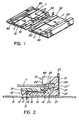
- Figure 1 illustrates a relatively large circuit board 10, hereafter referred to as the mother board, on which are mounted a series of small boards 11, hereafter referred to as daughter boards.
- the mother board On which are mounted a series of small boards 11, hereafter referred to as daughter boards.
- Components and devices of various types are mounted and/or formed on the daughter boards.
- conductor patterns are formed on the mother board with contact positions to which contact is to be made from daughter boards.
- the conductor patterns on the mother board interconnect the daughter boards and also provide input and output connections to other parts of a system.
- Figure 2 is a cross-section through one edge of a daughter board and part of a mother board, and a connector.
- the connector has two assemblies or main members, an elongate first member, hereinafter referred to as a bottom member 12 and an elongate second member, hereinafter referred to as a top member 13.
- the bottom member 12 has two parts, a base 14 and a cap 15. Between the base and the cap are held a plurality of contacts 16.
- the contacts 16 have tail portions 17 which pass through the mother board 10 and can be soldered to conductor patterns 19 on the under surface of the mother board.
- the contacts 16 also have spring cantilever contact portions 18.
- the base is attached to the mother board 10.
- the top member 13 also has a base 20, extending along one edge of the daughter board, and a channel shaped member 21 which fits over the edge of the base 20. Between the base 20 and channel member 21 are held a plurality of contacts 22.
- the contacts 22 are generally U-shaped, having a top leg 23 which extends over the top surface of the daughter board 11 with the ends of the legs soldered to contact pads on the daughter board, as illustrated at 24.
- a bottom leg 25 of each contact 22 extends beneath the base 20, and makes contact with the cantilever contact portion 18 of a related contact 16.
- a spring member 26 has its lower end 27 bent to extend under the base 14 of the bottom member 12.
- the spring member extends up past the edges of the base 14 and the channel member 21 and has a top portion bent over in the form of a hook 28.
- the hook 28 snaps over the top of the channel member 21 and holds the top member 13 on the bottom member 12. This maintains connections between the contacts 16 and 22.
- a connector is provided at the opposite edges of a daughter board and then the daughter board is held in position on the mother board. If desired, a metal protector member 29 can be provided on the channel member 21. The top member 13, and the daughter board, are released by pulling back the spring member 26.
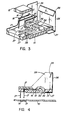
- Figures 3 and 4 illustrate the bottom member 12 in more detail, Figure 3 illustrating the individual items and Figure 4 showing the assembly.
- the base 14 has a comb formation formed by a laterally extending rib 35 in which are formed slots 36.
- the slots are extended in the base top surface, in the form of grooves 37, to holes 38 through which the tail portions 17 of the contacts 16 pass.
- the slots 36 and grooves 37 position the contacts 16 along the connector.
- An upwardly extending web 39 at each end of the base 14, act to locate the cap 15, and also the top member 13.
- the cap 15 holds the contacts 16 down in the grooves 37 with the face ends of the contacts positioned in the comb formation. In the relaxed condition the contact portions 18 are positioned up from the bottom surfaces of the slots 36.
- FIGs 5 and 6 illustrate the top member 13 in more detail.
- the base 20 is formed with shallow grooves 40 extending down a front edge 41 and over a top surface 42.
- a comb formation is formed in the bottom surface of the base by slots 43, the slots 43 dimensional and spaced to accept the parts of rib 35 of the bottom member between the slots 36.
- the contacts 22 fit in the grooves 40 on the front edge 41 and top surface 42 and along the bottom surface between the slots 43.
- the ends of the bottom legs 25 fit into recesses 44 in the base.
- the channel member 21 has a longitudinal groove 45 which is a tight fit over the front portion of the base when the contacts 22 are assembled thereon.
- the contacts are positioned on the base, sitting in the grooves 40, and the channel member 21 is pushed on, holding the contacts in position.
- This sub-assembly is normally supplied in an assembled condition.
- the daughter board and top member 13 are then assembled by sliding the top members on to the edge of the daughter board.
- the daughter board is located by rib 48 extending up at each end of the base 20. Small pins may be inserted through aligned holes in the ribs 48 and board 11 to retain in assembled condition.
- the ends of the upper legs 23 of the contacts 22 are then soldered to the contact pads on the daughter board, as by vapour phase soldering.
- Figure 7 illustrates modifications of the connector illustrated in Figure 2.
- No metal protector member is provided on the channel member, and a laterally extending recess 46 extends along the top edge of the channel member at its front surface.
- the hook 28 of the spring 26 snaps into the recess 46.
- the lower end 27 of the spring is inserted into a slot 47 in the base 14, instead of fitting under the base.
- a connector is provided at opposite edges of a daughter board.
- connectors are indicated generally" at 50.
- the bottom members 12 are attached to'the mother board at predetermined positions, with the top members attached to opposite edges of daughter boards.
- a daughter board is mounted on the mother board by positioning one edge on the mother board, the daughter board inclined upward slightly. This will engage one channel member 21 under the hook 28 at that end. The daughter board is then rotated down and the outer edge of the channel member at the other edge will deflect the spring member 26 outward by pushing the hook outward. When the daughter board is fully in position, the hook will snap over.
- the bottom legs 25 of the contacts 22 engage with and push down the cantilever portions 18 of the contacts 16. Removal of a daughter board is obtained by pulling back a spring 26 and lifting the daughter board at that edge. The board can then be disengaged at the other edge.
- the base 14 of the bottom member 12 is attached by screws extending up through the mother board into the base.
- the screws pass through holes in the lower end 27 of the spring.
- the positioning of the base 14 on the mother board 10 is initially provided by circular bosses on the bottom surface of the base which fit into holes in the mother board to give accurate location. This is seen at 51 in Figure 7.
- a simple way of obtaining this is to form a small protrusion at each end of a base at the front edge.
- a corresponding recess is formed at each end of a channel member.
- a base with protrusions is then positioned on the mother board to coincide with the channel member on a daughter board which has recesses. The channel member at the other edge of the daughter board would not have recesses and therefore complete assembly could not be obtained if the daughter board was not correctly oriented.
- Figure 8 illustrates an alternative form of base 14 and Figures 9 to 12 illustrate an alternative form of cap 15 to meet the base 14 of Figure 8.
- the base 14 is molded with the spring 26 molded in situ. Holes 55 are formed in the lower end 27 of the spring, these holes 55 positioned to align with attachment holes 56 through the base. Slots 36 and grooves 37 are provided, as in the other forms of base, but in this example they extend to the edge of the base and cooperate with grooves 57 and 57a at the inner edge of the base. The tails 17 of the contacts are bent down to extend down the grooves 57 and 57a as indicated in dotted outline.
- the cap 15 illustrated in Figures 9 to 12 has a comb formation at 58 which fits in the grooves 57 and 57a of the base.
- Two projections 59 fit into apertures in the base 14 to locate the cap relative to the base.
- the comb formation holds the contacts 16 in position during and after assembly of the bottom member.
- Figure 13 illustrates a daughter board 11 mounted on a mother board 10, with a connector at each end.
- the contact positions between the contacts 16 and 22 is inboard of the edge of the upper or daughter board, and even further inboard of the outer edge or surface of the member 21. Under some conditions this can produce an undesirable bonding moment on the daughter board, the board and channel member pivotting about the contact position of the hook 28 with the channel member 21.
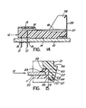
- Figures 14,15 and 16 illustrate a modification to the contacts 16 and 22, and the base 14 and channel member 21 which moves the contact position between the contacts 16 and 22 outboard of the edge of the daughter board 11 and almost in line with the contact between hook and channel member.
- the same reference numerals are used for the same or similar items.
- Figure 14 illustrates a modified form of bottom member, particularly a modified form of the base 14.
- the base has a plurality of grooves or slots 37, the slots 37 forming a shallow comb formation.
- the contacts 16 are of straight cantilever form, with contact portions 18 and tail portions 17 which pass through the mother board 10.
- a cap 15 fits on the base 14, and is attached thereto.
- a spring member of hook 27 is provided, as in Figure 7, molded integral with the base.
- Figure 15 illustrates a modified top member 13, both the base 20 and member 21 being modified.
- Member 21 no longer forms a channel for receiving the base, only having a recess 65 on its front wall.
- the lower edge 66 of member 21 forms a slotted web 67 which extends along the member, forming a shallow comb formation having ribs and slots, the web having a convex arcuate surface leading to a further recess 69 along the bottom of the rear wall.
- the base 20 has a shallow channel shaped recess 67 which receives the edge of the daughter board and has a plurality of parallel grooves running over the top edge and down the outer edge.
- Contacts 22 are positioned in these grooves, the contacts extending down at the ends of upper legs 23 to make contact with contact pads on the daughter board.
- the lower legs 25 are bent outward and have a curved formation 70 to fit closely on the ribs at the slotted web 67.
- the contacts 22 are usually assembled to the base 20, resting in the grooves in the top edge and outer edge. The member 21 is pushed on, the curved formations 70 snapping over the slotted rib 67.
- bottom and top members 12 and 13 The assembly of bottom and top members 12 and 13 is illustrated in Figure 16.
- the slotted rib fits into the slots 37 and the curved parts 70 of the contacts 22 push down on the contact portions 18 of contacts 16, the contact portions 18 being pushed down into the slots 37. It will be seen that the contact position between 16 and 22 is outboard of the edge of the daughter board and is also not far from being aligned with the contact position of the hook 28 with member 21.
- Figures 17 and 18 illustrate one way of obtaining polarization and keying.
- a channel member as in Figures 5 and 6 apertures 75 are formed.
- pins 76 can be pushed.
- slotted apertures 77 are formed, into which pins 78 can be pushed. The pins 76 can enter the slots of apertures 77, but will be prevented from so entering if a pin 78 is inserted into an aperture 77.
- pins 76 and pins 78 By suitable positioning of pins 76 and pins 78, a variety of codings or arrangements can be provided. With two apertures 75 each end of member 21 and two apertures 77 in each rib 39, fifteen distinct codes can be formed. More apertures will considerably increase the number of codes.
- the connector has a very low profile, no higher than the height over components mounted on the daughter board.
- the contacts 22 can be at a close pitch, for example 0.05 in (1.27 mm), while by staggering the tails 17 of contacts 16, the pitch of the contact areas of the conductor patterns 19 on the mother board can be 0.1 in (2.54 mm).
- the connectors at each of a daughter board extend beyond the edges of the daughter board by a very small amount and very little clearance is required between connectors for adjacent daughter boards. Sufficient clearance to move a spring 26 off the top member of a connector is all that is necessary. Very little space is required at the side of a daughter board also.
- the connectors can be as little as 0.060 in (1.524 mm) longer than a daughter board and can be mounted in end-to- end contact. A clearance of 0.050 in (1.27 mm) is sufficient between the spring 26.
- the overall height of a connector can be as low as 0.5 in (12.7 mm).
Landscapes
- Coupling Device And Connection With Printed Circuit (AREA)
Description
- This relates to a high density low profile multiple contact connector. Such a connector is particularly applicable to circuit boards. A particular use is for mounting sub-boards, often referred to as daughter boards, on a large circuit board, often referred to as a mother board. The invention is particularly applicable to telecommunications systems.
- It is quite common to require the mounting of so-called daughter boards on the larger so-called mother boards. Electrical and electronic components are mounted on a daughter board which is then mounted on the mother board. With the increased density which is being achieved, the number of contacts, or connections, to be made between mother board and daughter is very high. In many cases it is desired to mount daughter boards on mother boards which must fit in very restricted spaces in a frame. In fact, the space available is often the same as for a circuit board carrying components directly on the board. Thus what can be termed the vertical height, that is the distance normal to the plane of the mother board, is severely restricted. This causes problems in providing connectors on the mother board for connection of the daughter boards.
- In the disclosure of EP-A-0034081 a connector for printed circuit boards having multiple contact members is described, comprising: an elongate bottom member for attachment to a circuit board; a plurality of spring contact members including a cantilever contact portion extending over a top surface of the bottom member and also a tail portion extending throughout the bottom member for passage through the circuit board; an elongate top member for attachment to an edge of a further circuit board; a plurality of contact members spaced apart along the top member, each contact member having an outer leg and having an inner leg which makes contact with contact pads on the further circuit board, the outer legs making contact with the cantilever contact portions of the contact members in the bottom member on assembly of the top and bottom members together. The connector also comprises a spring member extending up from the bottom member along an outer edge and including a top portion adapted to extend over the outer edge of the top member and retain the top member on the bottom member. The present invention differs from the above disclosure in that only the upper surface of the second circuit board is connected to the first circuit board, connection of the two contact members is made below the plane of the scond circuit board, and the
bottom member 12 has abase 14 and acap 15, positioned on the base, thecap 15 attached to thebase 14 and holding thecontact members 16 in position in thelower member 12. - European Patent 0030763 discloses a connector for interconnecting large scale integration (LSI) circuit packages having a plurality of conductive interfaces with a printed circuit board. The circuit includes a plurality of latches moveable on a ramp of dielectrics housing containing a plurality of contact springs whereby movement of the latch out of a ramp valley causes it to clamp onto the upper surfaces of the circuit package and forces the lower surfaces of the circuit package, containing the conductive interfaces to electrically contact the contact springs in the housing. As in the present invention, the above Patent describes a spring member including an inwardly extending flange at its lower end, which is positioned in a slot extending from an outer edge of the bottom member (housing); the spring member has the function of directly clamping the circuit package to the housing and facilitating electrical contact between the spring contact members and the lower surface of the circuit package. However, in the present invention the spring member is provided to maintain the top (13) and bottom (12) members of the housing in an assembled condition. Additionally, rather than applying the second circuit board to the connector, as in the above disclosure, in the present invention the daughter board and
top member 13 are assembled by sliding the top members onto the edge of the daughter board. The daughter board is located in theupper member 13 by ribs extending up at each end of the base (Fig. 6) and may be secured in position by small pins inserted through aligned bores in theribs 48 and board 11. An advantage of the present invention therefore is thattop member 13 and daughter boards 11 may be assembled in advance of the complete assembly of the connector and remotely from the mother board, facilitating easier and more effective joining (soldering) of thecontact members 22 to contacts on the upper surface of the daughter board 11 at 24. - The present invention provides a connector which has a very low height profile, extends only a very minimal distance beyond the periphery of a daughter board, permitting other daughter boards to be mounted very close. The connector has a high density contact arrangement, provides snap-in mounting and can be provided with keying to ensure corrected orientation of a daughter board on the mother board.
- Broadly, the present invention provides a multiple contact connector comprising:
- an elongate bottom member for attachment to a circuit board; a plurality of spring contact members spaced apart along the bottom member, each contact member including a cantilever contact portion extending over the top surface of the bottom member in a direction normal to the length of the bottom member and also including a tail portion extending through the bottom member for passage through the circuit board and connection to a circuit pattern on the circuit board;
- an entirely separate elongate top member for attachment to an edge of a further circuit board; a plurality of contact members of generally U-shaped form spaced apart along the top member, each contact member having a bottom leg extending over a bottom surface of the top member in a direction normal to the length of the top member, and having a top leg, spaced apart from the bottom leg, extending from the top member to make contact with contact pads on the further circuit board, the bottom legs of the contact member positioned to make contact with the cantilever contact portions of the contact members in the bottom member on assembly of the top and bottom members together; and
- a spring member extending up from the bottom member along an outer edge and including a top portion adapted to extend over the outer edge of the top member and retain the top member on the bottom member.
- Normally a connector is provided on opposite edges of a smaller board, the springs retaining the smaller board in position on the larger board.
- The invention will be readily understood by the following description of certain embodiments, in conjunction with the accompanying drawings, in which:-
- Figure 1 is a perspective view of a large, or mother, board with several smaller, or daughter, boards mounted thereon;
- Figure 2 is a cross-section through a connector, on a mother board with a daughter board, on the line II-II of Figure 1;
- Figure 3 is an exploded perspective view of a bottom member of a connector;
- Figure 4 is a cross-section of the bottom member of Figure 3 in an assembled state, on the same line as Figure 2;
- Figure 5 is an exploded perspective view of a top member of a connector;
- Figure 6 is a cross-section of the top member of Figure 5 in an assembled state, on the same line as Figure 2;
- Figure 7 is a cross-section similar to that of Figure 2, illustrating some modifications;
- Figure 8 is a cross-section through an alternative form of a base for a bottom member;
- Figure 9 is a bottom plan view, in the direction of arrow A in Figure 10, of a cap to suit the base of Figure 8;
- Figure 10 is an end view in the direction of arrow B in Figure 9;
- Figures 11 and 12 are cross-sections on the lines XI-XI and XII-XII respectively, on Figure 10; and
- Figure 13 is a cross-section through a daughter board mounted on a mother board, with a connector at each end of the daughter board.
- Figure 14 is a cross-sectional view similar to that of Figure 4, of an alternative form of bottom member;
- Figure 15 is a cross-sectional view, similar to that of Figure 6, of an alternative form of top member;
- Figure 16 is a cross-sectional view, similar to those of Figures 2 and 7, illustrating the assembly of top and bottom members of Figures 15 and 14 respectively; and
- Figures 17 and 18 are perspective views on an end of a top member and a bottom member respectively, illustrating polarity and keying provisions.
- Figure 1 illustrates a relatively
large circuit board 10, hereafter referred to as the mother board, on which are mounted a series of small boards 11, hereafter referred to as daughter boards. One example of use of such arrangements is in telecommunications systems. Components and devices of various types are mounted and/or formed on the daughter boards. As the density of mounting of such components and devices, and as the density of components in a device, such as large scale and very large scale integrated circuit devices increases, the problem of providing connections and interconnections to the components and devices becomes more difficult. In the arrangement as in Figure 1, conductor patterns are formed on the mother board with contact positions to which contact is to be made from daughter boards. The conductor patterns on the mother board interconnect the daughter boards and also provide input and output connections to other parts of a system. - To obtain as high a density as possible on the mother board, very close positioning of the daughter boards is desired. At the same time, it is necessary to keep the overall height of any connector to a minimum. Often the mother boards are to be inserted into frames having a preset pitch between boards. Thus the connectors must have a low profile. As illustrated in Figure 1, with connectors in accordance with the present invention, daughter boards can be mounted with minimal clearance. The connectors in Figure 1 are only illustrated in a generalized form, being shown in more detail in Figures 2 to 13.
- Figure 2 is a cross-section through one edge of a daughter board and part of a mother board, and a connector. The connector has two assemblies or main members, an elongate first member, hereinafter referred to as a
bottom member 12 and an elongate second member, hereinafter referred to as atop member 13. Thebottom member 12 has two parts, abase 14 and acap 15. Between the base and the cap are held a plurality ofcontacts 16. Thecontacts 16 havetail portions 17 which pass through themother board 10 and can be soldered toconductor patterns 19 on the under surface of the mother board. Thecontacts 16 also have springcantilever contact portions 18. The base is attached to themother board 10. - The
top member 13 also has abase 20, extending along one edge of the daughter board, and a channel shapedmember 21 which fits over the edge of thebase 20. Between thebase 20 andchannel member 21 are held a plurality ofcontacts 22. Thecontacts 22 are generally U-shaped, having atop leg 23 which extends over the top surface of the daughter board 11 with the ends of the legs soldered to contact pads on the daughter board, as illustrated at 24. Abottom leg 25 of eachcontact 22 extends beneath thebase 20, and makes contact with thecantilever contact portion 18 of arelated contact 16. - A
spring member 26 has itslower end 27 bent to extend under thebase 14 of thebottom member 12. The spring member extends up past the edges of thebase 14 and thechannel member 21 and has a top portion bent over in the form of ahook 28. Thehook 28 snaps over the top of thechannel member 21 and holds thetop member 13 on thebottom member 12. This maintains connections between thecontacts metal protector member 29 can be provided on thechannel member 21. Thetop member 13, and the daughter board, are released by pulling back thespring member 26. - Figures 3 and 4 illustrate the
bottom member 12 in more detail, Figure 3 illustrating the individual items and Figure 4 showing the assembly. As seen in Figure 3, thebase 14 has a comb formation formed by a laterally extendingrib 35 in which are formedslots 36. The slots are extended in the base top surface, in the form ofgrooves 37, toholes 38 through which thetail portions 17 of thecontacts 16 pass. Theslots 36 andgrooves 37 position thecontacts 16 along the connector. An upwardly extendingweb 39 at each end of thebase 14, act to locate thecap 15, and also thetop member 13. When assembled, as illustrated in Figure 4, thecap 15 holds thecontacts 16 down in thegrooves 37 with the face ends of the contacts positioned in the comb formation. In the relaxed condition thecontact portions 18 are positioned up from the bottom surfaces of theslots 36. - Figures 5 and 6 illustrate the
top member 13 in more detail. In Figure 5 the various individual items are illustrated. Thebase 20 is formed withshallow grooves 40 extending down afront edge 41 and over atop surface 42. A comb formation is formed in the bottom surface of the base byslots 43, theslots 43 dimensional and spaced to accept the parts ofrib 35 of the bottom member between theslots 36. Thecontacts 22 fit in thegrooves 40 on thefront edge 41 andtop surface 42 and along the bottom surface between theslots 43. The ends of thebottom legs 25 fit intorecesses 44 in the base. - The
channel member 21 has alongitudinal groove 45 which is a tight fit over the front portion of the base when thecontacts 22 are assembled thereon. To assemble, the contacts are positioned on the base, sitting in thegrooves 40, and thechannel member 21 is pushed on, holding the contacts in position. This sub-assembly is normally supplied in an assembled condition. The daughter board andtop member 13 are then assembled by sliding the top members on to the edge of the daughter board. The daughter board is located byrib 48 extending up at each end of thebase 20. Small pins may be inserted through aligned holes in theribs 48 and board 11 to retain in assembled condition. The ends of theupper legs 23 of thecontacts 22 are then soldered to the contact pads on the daughter board, as by vapour phase soldering. - Figure 7 illustrates modifications of the connector illustrated in Figure 2. No metal protector member is provided on the channel member, and a laterally extending
recess 46 extends along the top edge of the channel member at its front surface. Thehook 28 of thespring 26 snaps into therecess 46. Thelower end 27 of the spring is inserted into a slot 47 in thebase 14, instead of fitting under the base. - As stated, a connector is provided at opposite edges of a daughter board. In Figure 1, connectors are indicated generally" at 50. The
bottom members 12 are attached to'the mother board at predetermined positions, with the top members attached to opposite edges of daughter boards. A daughter board is mounted on the mother board by positioning one edge on the mother board, the daughter board inclined upward slightly. This will engage onechannel member 21 under thehook 28 at that end. The daughter board is then rotated down and the outer edge of the channel member at the other edge will deflect thespring member 26 outward by pushing the hook outward. When the daughter board is fully in position, the hook will snap over. As the daughter board is mounted, thebottom legs 25 of thecontacts 22 engage with and push down thecantilever portions 18 of thecontacts 16. Removal of a daughter board is obtained by pulling back aspring 26 and lifting the daughter board at that edge. The board can then be disengaged at the other edge. - The
base 14 of thebottom member 12 is attached by screws extending up through the mother board into the base. The screws pass through holes in thelower end 27 of the spring. The positioning of the base 14 on themother board 10 is initially provided by circular bosses on the bottom surface of the base which fit into holes in the mother board to give accurate location. This is seen at 51 in Figure 7. - If necessary, to ensure that a daughter board is mounted the right way round, that is, with correct orientation, keying can be provided. A simple way of obtaining this is to form a small protrusion at each end of a base at the front edge. A corresponding recess is formed at each end of a channel member. A base with protrusions is then positioned on the mother board to coincide with the channel member on a daughter board which has recesses. The channel member at the other edge of the daughter board would not have recesses and therefore complete assembly could not be obtained if the daughter board was not correctly oriented.
- Figure 8 illustrates an alternative form of
base 14 and Figures 9 to 12 illustrate an alternative form ofcap 15 to meet thebase 14 of Figure 8. - As illustrated in Figure 8, the
base 14 is molded with thespring 26 molded in situ.Holes 55 are formed in thelower end 27 of the spring, theseholes 55 positioned to align with attachment holes 56 through the base.Slots 36 andgrooves 37 are provided, as in the other forms of base, but in this example they extend to the edge of the base and cooperate withgrooves 57 and 57a at the inner edge of the base. Thetails 17 of the contacts are bent down to extend down thegrooves 57 and 57a as indicated in dotted outline. - The
cap 15 illustrated in Figures 9 to 12 has a comb formation at 58 which fits in thegrooves 57 and 57a of the base. Twoprojections 59 fit into apertures in the base 14 to locate the cap relative to the base. The comb formation holds thecontacts 16 in position during and after assembly of the bottom member. - Figure 13 illustrates a daughter board 11 mounted on a
mother board 10, with a connector at each end. - In the contact arrangements illustrated in Figures 2 to 13, the contact positions between the
contacts member 21. Under some conditions this can produce an undesirable bonding moment on the daughter board, the board and channel member pivotting about the contact position of thehook 28 with thechannel member 21. - Figures 14,15 and 16 illustrate a modification to the
contacts base 14 andchannel member 21 which moves the contact position between thecontacts - Figure 14 illustrates a modified form of bottom member, particularly a modified form of the
base 14. The base has a plurality of grooves orslots 37, theslots 37 forming a shallow comb formation. Thecontacts 16 are of straight cantilever form, withcontact portions 18 andtail portions 17 which pass through themother board 10. Acap 15 fits on thebase 14, and is attached thereto. A spring member ofhook 27 is provided, as in Figure 7, molded integral with the base. - Figure 15 illustrates a modified
top member 13, both thebase 20 andmember 21 being modified.Member 21 no longer forms a channel for receiving the base, only having arecess 65 on its front wall. Thelower edge 66 ofmember 21 forms a slottedweb 67 which extends along the member, forming a shallow comb formation having ribs and slots, the web having a convex arcuate surface leading to afurther recess 69 along the bottom of the rear wall. Thebase 20 has a shallow channel shapedrecess 67 which receives the edge of the daughter board and has a plurality of parallel grooves running over the top edge and down the outer edge.Contacts 22 are positioned in these grooves, the contacts extending down at the ends ofupper legs 23 to make contact with contact pads on the daughter board. Thelower legs 25 are bent outward and have a curved formation 70 to fit closely on the ribs at the slottedweb 67. Thecontacts 22 are usually assembled to thebase 20, resting in the grooves in the top edge and outer edge. Themember 21 is pushed on, the curved formations 70 snapping over the slottedrib 67. - The assembly of bottom and
top members slots 37 and the curved parts 70 of thecontacts 22 push down on thecontact portions 18 ofcontacts 16, thecontact portions 18 being pushed down into theslots 37. It will be seen that the contact position between 16 and 22 is outboard of the edge of the daughter board and is also not far from being aligned with the contact position of thehook 28 withmember 21. - It is often desirable to ensure that daughter boards are positioned on mother boards the right way round-polarized, and also that the correct daughter board is attached to the mother board--keying. Figures 17 and 18 illustrate one way of obtaining polarization and keying. In each end surface of
member 21, in Figure 17 a channel member as in Figures 5 and 6apertures 75 are formed. Into these apertures pins 76 can be pushed. In the top of theweb 39 at each end of thebase 14, slottedapertures 77 are formed, into which pins 78 can be pushed. Thepins 76 can enter the slots ofapertures 77, but will be prevented from so entering if apin 78 is inserted into anaperture 77. It will be appreciated that by suitable positioning ofpins 76 and pins 78, a variety of codings or arrangements can be provided. With twoapertures 75 each end ofmember 21 and twoapertures 77 in eachrib 39, fifteen distinct codes can be formed. More apertures will considerably increase the number of codes. - The connector has a very low profile, no higher than the height over components mounted on the daughter board. The
contacts 22 can be at a close pitch, for example 0.05 in (1.27 mm), while by staggering thetails 17 ofcontacts 16, the pitch of the contact areas of theconductor patterns 19 on the mother board can be 0.1 in (2.54 mm). - The connectors at each of a daughter board extend beyond the edges of the daughter board by a very small amount and very little clearance is required between connectors for adjacent daughter boards. Sufficient clearance to move a
spring 26 off the top member of a connector is all that is necessary. Very little space is required at the side of a daughter board also. The connectors can be as little as 0.060 in (1.524 mm) longer than a daughter board and can be mounted in end-to- end contact. A clearance of 0.050 in (1.27 mm) is sufficient between thespring 26. The overall height of a connector can be as low as 0.5 in (12.7 mm).
Claims (16)
Applications Claiming Priority (4)
| Application Number | Priority Date | Filing Date | Title |
|---|---|---|---|
| US06/566,037 US4527848A (en) | 1983-12-27 | 1983-12-27 | High density low profile multiple contact connector |
| US566037 | 1983-12-27 | ||
| US06/618,886 US4530554A (en) | 1983-12-27 | 1984-06-08 | High density low profile multiple contact connector |
| US618886 | 1984-06-08 |
Publications (3)
| Publication Number | Publication Date |
|---|---|
| EP0147092A2 EP0147092A2 (en) | 1985-07-03 |
| EP0147092A3 EP0147092A3 (en) | 1987-01-21 |
| EP0147092B1 true EP0147092B1 (en) | 1990-11-28 |
Family
ID=27074044
Family Applications (1)
| Application Number | Title | Priority Date | Filing Date |
|---|---|---|---|
| EP84308414A Expired - Lifetime EP0147092B1 (en) | 1983-12-27 | 1984-12-04 | High density low profile multiple contact connector |
Country Status (4)
| Country | Link |
|---|---|
| US (1) | US4530554A (en) |
| EP (1) | EP0147092B1 (en) |
| CA (1) | CA1213952A (en) |
| DE (1) | DE3483684D1 (en) |
Families Citing this family (14)
| Publication number | Priority date | Publication date | Assignee | Title |
|---|---|---|---|---|
| US4755907A (en) * | 1987-04-01 | 1988-07-05 | Gte Communication Systems Corporation | Substrate connector guide |
| US4755906A (en) * | 1987-04-01 | 1988-07-05 | Gte Communication Systems Corporation | Substrate connector guide |
| US4797786A (en) * | 1987-04-01 | 1989-01-10 | Gte Communication Systems Corporation | Substrate mounting device |
| GB8812330D0 (en) * | 1988-05-25 | 1988-06-29 | Thomas & Betts Corp | Connector for printed circuit boards |
| US4840570A (en) * | 1988-06-27 | 1989-06-20 | Teknekron Infoswitch Corporation | Plug-in card module |
| GB8908098D0 (en) * | 1989-04-11 | 1989-05-24 | Amp Holland | Electrical jacks and headers |
| US4986778A (en) * | 1989-05-04 | 1991-01-22 | 501 Venturdyne, Ltd. | Carrier for use in testing circuit boards |
| US5220270A (en) * | 1992-04-24 | 1993-06-15 | Automatic Technologies, Inc. | Battery charging device with secured contact unit |
| US5324206A (en) * | 1992-07-31 | 1994-06-28 | Hughes Aircraft Company | Multimodule terminating plane assembly |
| US5273442A (en) * | 1992-12-24 | 1993-12-28 | The Whitaker Corporation | Modular chip carrier socket |
| JP2001110488A (en) * | 1999-08-04 | 2001-04-20 | Japan Aviation Electronics Industry Ltd | Connector structure for connection between boards |
| JP2003208939A (en) * | 2002-01-16 | 2003-07-25 | Yazaki Corp | Terminal mounting method and mounting structure |
| TWM241942U (en) * | 2003-01-24 | 2004-08-21 | Delta Electronics Inc | A casing structure for an electronic apparatus |
| DE102012011895A1 (en) * | 2012-06-15 | 2013-12-19 | Yamaichi Electronics Deutschland Gmbh | Connector and contact system |
Family Cites Families (7)
| Publication number | Priority date | Publication date | Assignee | Title |
|---|---|---|---|---|
| FR2114169A6 (en) * | 1970-11-18 | 1972-06-30 | Honeywell Bull | |
| AT339988B (en) * | 1973-03-23 | 1977-11-25 | Electrovac | CONTACT BAR |
| US3905670A (en) * | 1974-04-05 | 1975-09-16 | Itt | Actuated printed circuit connector |
| US3960424A (en) * | 1974-10-02 | 1976-06-01 | Amp Incorporated | Multi-contact spring connector for board to board connections |
| FR2469019A1 (en) * | 1979-10-26 | 1981-05-08 | Socapex | SUPPORT FOR PLUG-IN CARD WITH ELECTRICAL AND THERMAL CONNECTION |
| US4330163A (en) * | 1979-12-05 | 1982-05-18 | E. I. Du Pont De Nemours And Company | Zero insertion force connector for LSI circuit package |
| FR2475809A1 (en) * | 1980-02-07 | 1981-08-14 | Socapex | CONNECTOR BAR FOR CONNECTOR CARD, AND CONNECTOR PROVIDED WITH SUCH BARRETTES |
-
1984
- 1984-06-08 US US06/618,886 patent/US4530554A/en not_active Expired - Lifetime
- 1984-10-12 CA CA000465295A patent/CA1213952A/en not_active Expired
- 1984-12-04 EP EP84308414A patent/EP0147092B1/en not_active Expired - Lifetime
- 1984-12-04 DE DE8484308414T patent/DE3483684D1/en not_active Expired - Fee Related
Also Published As
| Publication number | Publication date |
|---|---|
| EP0147092A3 (en) | 1987-01-21 |
| EP0147092A2 (en) | 1985-07-03 |
| DE3483684D1 (en) | 1991-01-10 |
| CA1213952A (en) | 1986-11-12 |
| US4530554A (en) | 1985-07-23 |
Similar Documents
| Publication | Publication Date | Title |
|---|---|---|
| EP0602443B1 (en) | Printed circuit board mounting device for electrical connectors | |
| US5181854A (en) | Press-contact type electric connector for a flat, flexible cable | |
| US3815077A (en) | Electrical connector assembly | |
| EP0409590B1 (en) | A board-surface mounting electric connector | |
| US4717218A (en) | Electric circuit board assembly | |
| EP0482669B1 (en) | Electrical connector and method of making an electrical connector | |
| US4530554A (en) | High density low profile multiple contact connector | |
| EP0166526B1 (en) | Chip carrier socket and contact | |
| KR970000291Y1 (en) | Surface mount electrical connector assembly | |
| EP0463487B1 (en) | Board-to-board connection type electric connector | |
| US5076804A (en) | Electrical connector assembly for mounting on a printed circuit board | |
| US5226824A (en) | IC socket and contact therein | |
| US4527848A (en) | High density low profile multiple contact connector | |
| JP3620833B2 (en) | Module connector | |
| JPH07211370A (en) | Electric connector to be mounted on printed circuit board | |
| KR970002447B1 (en) | Terminals for Surface Mount Electrical Connectors | |
| US4417095A (en) | Support member for electronic devices | |
| JP2741865B2 (en) | Electrical connector | |
| US6716060B2 (en) | Electrical connector with solder plate and pegs for PC board mounting | |
| EP0171985B1 (en) | Improvements in stacking connectors for printed circuit boards and in printed circuit board assemblies employing stacking connectors | |
| US4968259A (en) | High density chip carrier socket | |
| EP0342873A2 (en) | Surface mount connector | |
| EP0385019B1 (en) | Electrical connector having preloaded terminals and method of manufacture | |
| US6068510A (en) | Electrical card connector | |
| EP0366744B1 (en) | Improved retention means for chip carrier sockets |
Legal Events
| Date | Code | Title | Description |
|---|---|---|---|
| PUAI | Public reference made under article 153(3) epc to a published international application that has entered the european phase |
Free format text: ORIGINAL CODE: 0009012 |
|
| AK | Designated contracting states |
Designated state(s): DE FR GB |
|
| PUAL | Search report despatched |
Free format text: ORIGINAL CODE: 0009013 |
|
| AK | Designated contracting states |
Kind code of ref document: A3 Designated state(s): DE FR GB |
|
| 17P | Request for examination filed |
Effective date: 19870310 |
|
| 17Q | First examination report despatched |
Effective date: 19880714 |
|
| GRAA | (expected) grant |
Free format text: ORIGINAL CODE: 0009210 |
|
| AK | Designated contracting states |
Kind code of ref document: B1 Designated state(s): DE FR GB |
|
| PGFP | Annual fee paid to national office [announced via postgrant information from national office to epo] |
Ref country code: GB Payment date: 19901203 Year of fee payment: 7 |
|
| PGFP | Annual fee paid to national office [announced via postgrant information from national office to epo] |
Ref country code: FR Payment date: 19901215 Year of fee payment: 7 |
|
| ET | Fr: translation filed | ||
| REF | Corresponds to: |
Ref document number: 3483684 Country of ref document: DE Date of ref document: 19910110 |
|
| PGFP | Annual fee paid to national office [announced via postgrant information from national office to epo] |
Ref country code: DE Payment date: 19910131 Year of fee payment: 7 |
|
| PLBE | No opposition filed within time limit |
Free format text: ORIGINAL CODE: 0009261 |
|
| STAA | Information on the status of an ep patent application or granted ep patent |
Free format text: STATUS: NO OPPOSITION FILED WITHIN TIME LIMIT |
|
| 26N | No opposition filed | ||
| PG25 | Lapsed in a contracting state [announced via postgrant information from national office to epo] |
Ref country code: GB Effective date: 19911204 |
|
| GBPC | Gb: european patent ceased through non-payment of renewal fee | ||
| PG25 | Lapsed in a contracting state [announced via postgrant information from national office to epo] |
Ref country code: FR Effective date: 19920831 |
|
| PG25 | Lapsed in a contracting state [announced via postgrant information from national office to epo] |
Ref country code: DE Effective date: 19920901 |
|
| REG | Reference to a national code |
Ref country code: FR Ref legal event code: ST |